

Page 1

NCP81246
l
Three-Rail Controller
with Intel Proprietary
Interface for IMVP8 CPU
Applications
The NCP81246 contains a two-phase, and two single-phase buck
regulators optimized for Intel IMVP8 compatible CPUs.
The two-phase controller combines true differential voltage sensing,
differential inductor DCR current sensing, input voltage feed-forward,
and adaptive voltage positioning to provide accurately regulated
power for IMVP8 Rail2.
The two single-phase controllers can be used for Rail1, Rail3 and
Rail4 rails. Both make use of ON Semiconductor’s patented enhanced
RPM operation. RPM control maximizes transient response while
allowing for smooth transitions between discontinuous frequency
scaling operation and continuous mode full power operation. The
single-phase rails have an ultralow offset current monitor amplifier
with programmable offset compensation for ultra high accuracy
current monitoring.
The NCP81246 offers three internal MOSFET drivers with a single
external PWM signal.
Two-Phase Rail Features
• Dual Edge Modulation for Fastest Initial Response to Transient
Loading
• High Performance Operational Error Amplifier
• Digital Soft Start Ramp
• Dynamic Reference Injection
• Accurate Total Summing Current Amplifier(Patent #US6683441)
• Dual High Impedance Differential Voltage and Total Current Sense
Amplifiers
• Phase-to-Phase Dynamic Current Balancing
• True Differential Current Balancing Sense Amplifiers for Each Phase
• Adaptive Voltage Positioning (AVP)
• Switching Frequency Range of 300 kHz – 750 kHz
• Vin range 4.5 V to 25 V
• Start-Up into Pre-Charged Loads While Avoiding False OVP
• UltraSonic Operation
• These Devices are Pb−Free, Halogen Free/BFR Free and are RoHS
Compliant
(Patent #US7057381)
onsemi.com
www.
521
QFN52
MN SUFFIX
CASE 485BE
MARKING DIAGRAM
NCP81246
FAWLYYWW
G
NCP81246 = Specific Device Code
F = Wafer Fab
A = Assembly Site
WL = Lot ID
YY = Year
WW = Work Week
G = Pb-Free Package
ORDERING INFORMATION
Device Package Shipping
NCP81246MNTXG QFN52
(Pb−Free)
†For information on tape and reel specifications,
including part orientation and tape sizes, please
refer to our Tape and Reel Packaging Specification
Brochure, BRD8011/D.
5000 / Tape & Ree
†
Single-Phase Rail Features
• Enhanced RPM Control System
• Ultra Low Offset IOUT Monitor
• Dynamic VID Feed-Forward
• Programmable Droop Gain
• Zero Droop Capable
Semiconductor Components Industries, LLC, 2017
February, 2018 − Rev. 6
• Thermal Monitor
• UltraSonic Operation
• Adjustable Vboot
• Digitally Controlled Operating Frequency
1 Publication Order Number:
NCP81246/D
Page 2
SKT_SNS+
SKT_SNS*
Batt chrgr
NCP81246
+5 V
+5 V
VCC
VSP
VSN
COMP
ILIM
IOUT
TSENSE
V
PU
NTC
V
PU
VRHOT
V
PU
SDIO
ALERT
SCLK
PSYS
GND
PVCC
BST
HG
SW
CSP
CSN
LG
V
IN
VCC_Rail1
NTC
SKT_SNS+
SKT_SNS*
SKT_SNS+
SKT_SNS*
V
TSENSE
BST
HG
NCP81246
NTC
IOUT
VSP
VSN
DIFFOUT
FB
COMP
EN
V
VRRDY
IN
VRMP
VSP
VSN
COMP
IOUT
ILIM
SW
CSP1
BST
HG
SW
CSP2
CSREF
CSSUM
ILIM
CSCOMP
PWM
DRON
CSP
CSN
LG
LG
NTC
VRDV
BST
PWM
HG
SW
EN
VCC
LG
NCP81253
V
IN
IN
VCC_Rail2
V
IN
VCC_Rail3
NTC
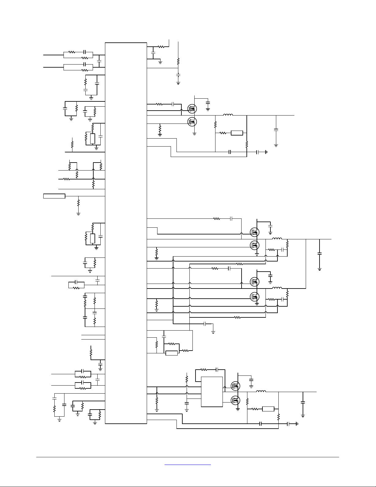
Figure 1. Application Schematic
www.onsemi.com
2
Page 3
NCP81246
VR_HOT#
SDIO
ALERT#
SCLK
VR_RDY
ROSC
ICCMAX_2PH
ICCMAX_1A
ICCMAX_1B
ADDR_VBOOT
TSENSE_2PH
TSENSE_1A
PSYS/TSENSE_1B
VRAMP
Thermal
Monitor
ENABLE
ENABLE
(VSP−VSN)
IOUT_2ph
IOUT_1a
IOUT_1b
VR Ready
Logic
Intel pro-
prietary
interface
Interface
& Logic
MUX
DRVON
PS#
ADC
OCP
OVP
Data
Registers
ENABLE
PS#
Oscillator
& RAMP
Generators
VRMP
VSP VSN
OVP
OVP
DAC
DAC
Feed-Forward
Current
Sense
OVP
AMP
MAX
OVP
DRVON
DIFF
AMP
−
+
+
−
DAC
Error
AMP
1.3 V
1.3 V
Buffer
IOUT
S
VSP
VSN
S
CSCOMP
−
+
Over-Current
Programming
Over-Current
Comparators
CSREF
VSP_2PH
VSN_2PH
DIFFOUT_2PH
FB_2PH
COMP_2PH
CSCOMP_2PH
CSSUM_2PH
CSREF_2PH
ILIM_2PH
OCP
IOUT_2PH
Current
Monitor
DRVON
VCC
EN
PVCC
GND
UVLO&EN
Comparators
ENABLE
OVP
OCP
PS#
PWM
Generators
PVM2
PS#
Power
State
Gate
COMP
PVM1
Zero Current
Detection
Current Balance
Amplifiers
IPH2
IPH1
ADDR_VBOOT
Config
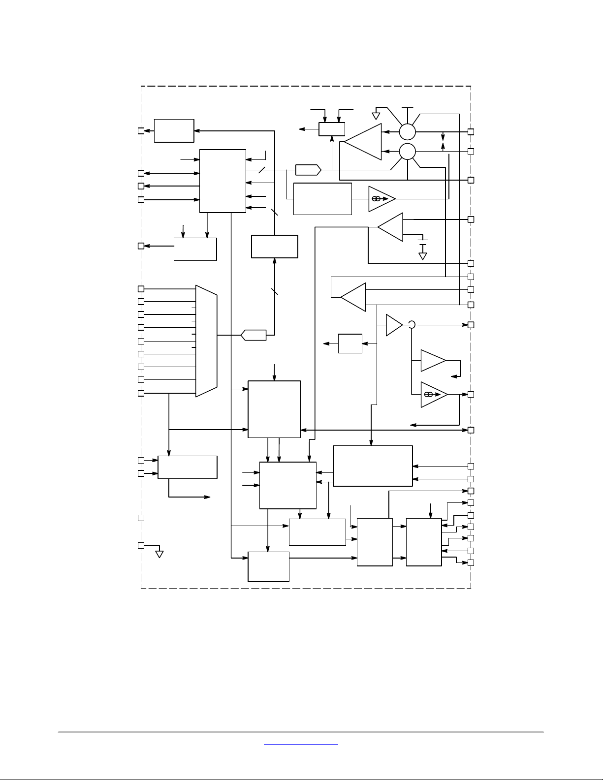
Figure 2. 2-Phase Rail Block Diagram
PVCC
Gate
Drivers
CSP2_2PH
CSP1_2PH
PWM
HG1
SW1
LG1
HG2
SW2
LG2
www.onsemi.com
3
Page 4
NCP81246
A
B
From Intel
proprietary
interface
Interface
VRMP
FREQ
DAC
DAC
Generator
DRVON
RAMP
DAC
Feed-Forward
COMP
PWM
Generator
RAMP
PWM
PS#
OVP
CURR
OCP
gm
Zero
Current
Detection
DAC Feed-Forward Current
DAC
OVP
OCP
+
AV = 1
OVP REF
OCP REF
IOUT
VSN
+
S
VSP
−
Droop
Current
+
Current
−
Sense AMP
Over-Current Programming
Over-Current
Comparators
Current
Monitor
ADDR_VBOOT
Config
Offset
Adjust
Gate
Driver
PVCC
Gate
Driver
PVCC
VSN_1x
VSP_1x
COMP_1x
CSP_1x
CSN_1x
ILIM_1x
IOUT_1x
HG3
SW3
LG3
PWM
HG2
SW2
LG2
1-Phase
Only
1-Phase
Only
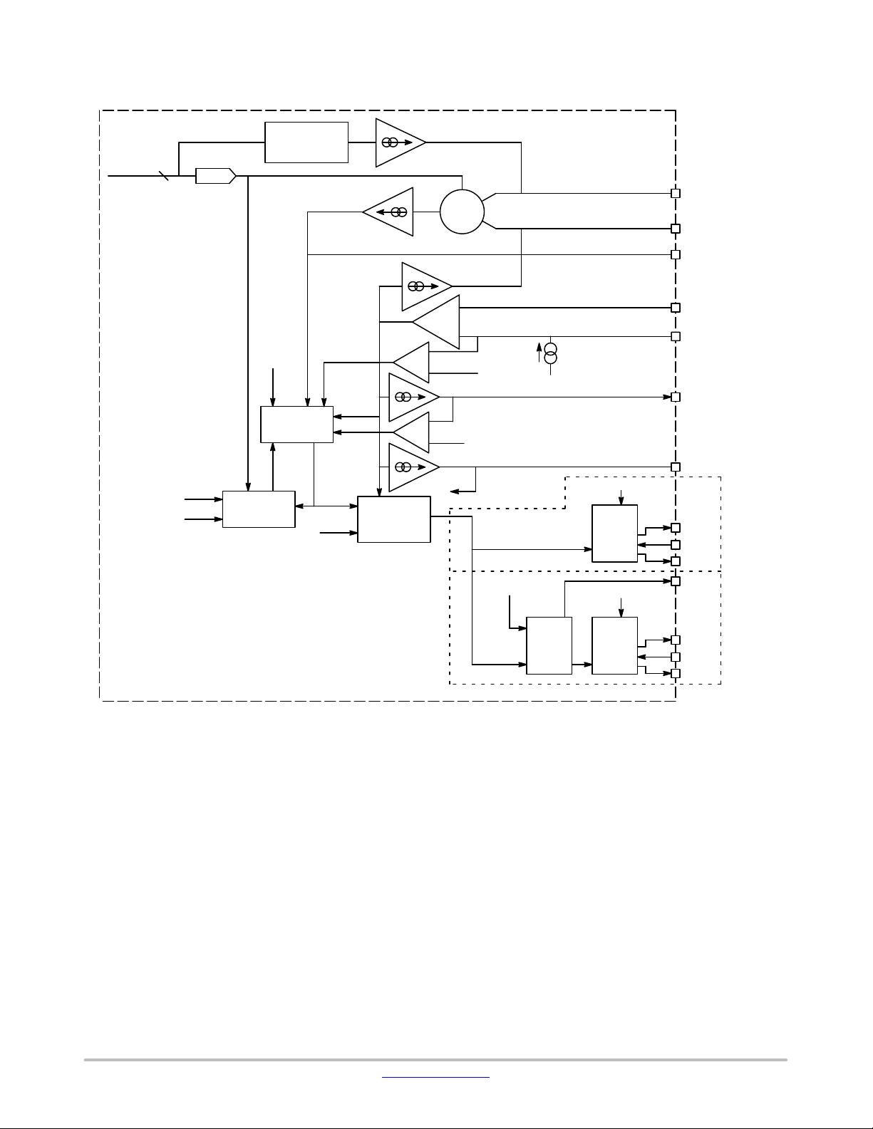
Figure 3. Single-Phase Block Diagram
www.onsemi.com
4
Page 5
IOUT_2ph
DIFFOUT_2ph/ICCMAX_2ph
FB_2ph
COMP_2ph
ILIM_2ph
CSCOMP_2ph
CSSUM_2ph
CSREF_2ph
CSP2_2ph
CSP1_2ph
TSENSE_2ph
VRMP
VCC
NCP81246
VSN_2ph
VSP_2ph
PSYS
VSP_1b
VSN_1b
COMP_1b
ILIM_1b
CSN_1b
CSP_1b
52515049484746454443424140
1
2
3
4
5
6
7
8
9
10
11
12
13
NCP81246
TAB: GROUND
(Not to Scale)
IOUT_1b
VR_RDYENPWM/ADDR_VBOOT
39
DRON
38
SCLK
37
ALERT#
36
SDIO
35
VR_HOT#
34
IOUT_1a
33
CSP_1a
32
CSN_1a
31
ILIM_1a
30
COMP_1a
29
VSN_1a
28
VSP_1a
27
TSENSE_1a
14151617181920212223242526
HG1
BST1
SW1
LG1/ROSC
PVCC
HG2
SW2
BST2
LG2/ICCMAX_1a
LG3/ICCMAX_1b
SW3
HG3
BST3
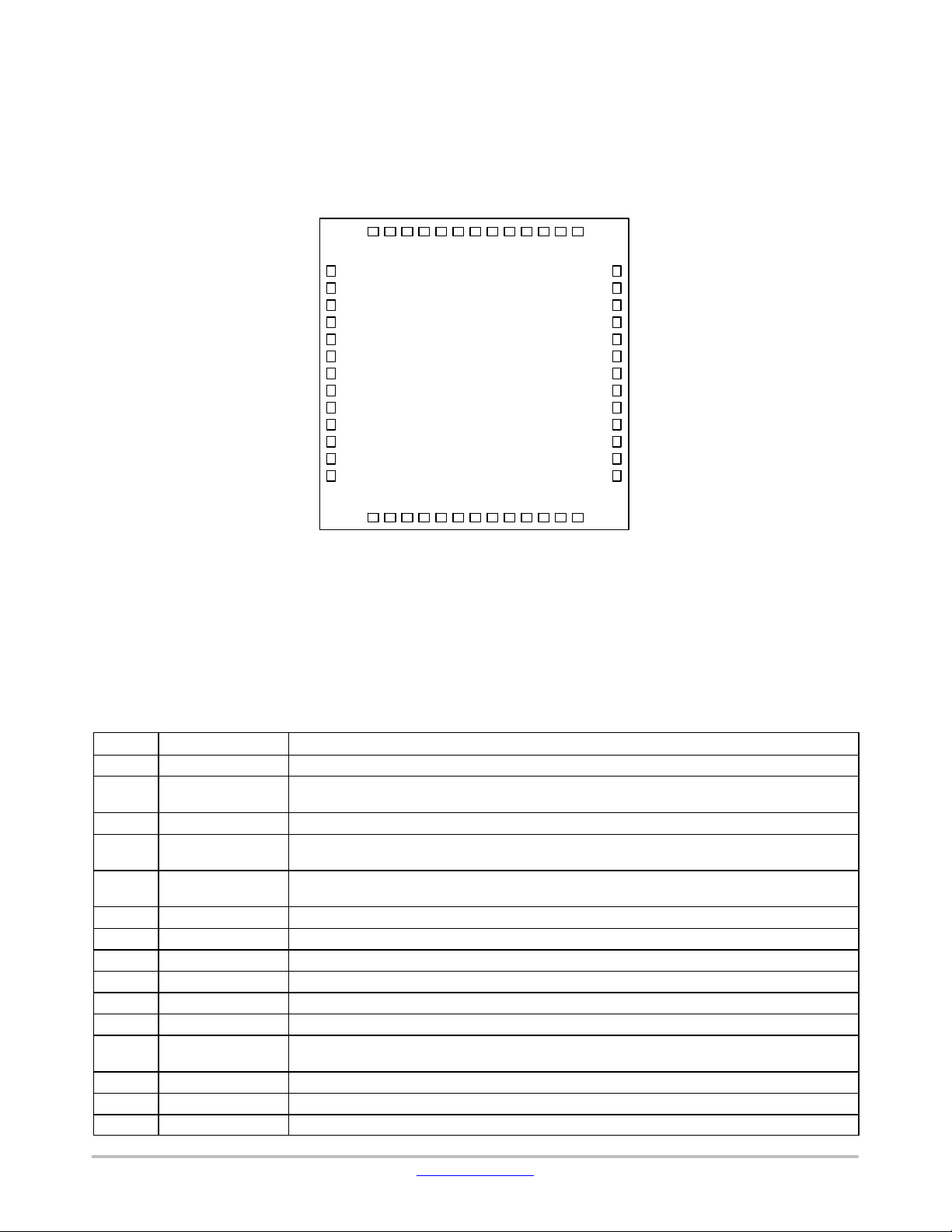
Figure 4. Pin Configuration
Table 1. NCP81246 PIN DESCRIPTIONS
Pin No.
1 IOUT_2ph A resistor to ground programs IOUT gain for the two-phase regulator.
2 DIFFOUT_2ph/
3 FB_2ph Error amplifier voltage feedback for two-phase regulator.
4 COMP_2ph Output of the error amplifier and the inverting inputs of the PWM comparators for two-phase
5 ILIM_2ph Over-current threshold setting − programmed with a resistor to CSCOMP_2ph for two-phase
6 CSCOMP_2ph Output of total-current-sense amplifier for two-phase regulator.
7 CSSUM_2ph Inverting input of total-current-sense amplifier for two-phase regulator.
8 CSREF_2ph Total-current-sense amplifier reference voltage input for two-phase regulator.
9 CSP2_2ph Non-inverting input to current-balance amplifier for Phase 2 of the two-phase regulator.
10 CSP1_2ph Non-inverting input to current-balance amplifier for Phase 1 of the two-phase regulator.
11 TSENSE_2ph Temperature sense input for the two-phase regulator.
12 VRMP Feed-forward input of Vin for the ramp-slope compensation. The current fed into this pin is used to
13 VCC Power for the internal control circuits. A decoupling capacitor is connected from this pin to ground.
14 BST1 High-side bootstrap supply for Phase 1 of the two-phase regulator.
15 HG1 High-side FET gate driver output for Phase 1 of the two-phase regulator.
Symbol Description
ICCMAX_2ph
Output of the two-phase regulator’s differential remote sense amplifier.
During start-up, the two-phase regulator’s ICCMAX is programmed with a pull-down on this pin.
regulator.
regulator.
control the ramp of the PWM slopes.
www.onsemi.com
5
Page 6

NCP81246
Table 1. NCP81246 PIN DESCRIPTIONS (continued)
Pin No. DescriptionSymbol
16 SW1 Current return for high-side FET gate driver for Phase 1 of the two-phase regulator.
17 LG1/ROSC Low-side FET gate driver output for Phase 1 of the two-phase regulator.
18 PVCC Power supply for all three internal FET gate drivers.
19 LG2/ICCMAX_1a Low-side FET gate driver output for Phase 2 of the two-phase regulator, or output of single-phase
20 SW2 Current return for high-side FET gate driver for Phase 2 of the two-phase regulator, or for
21 HG2 High-side FET gate driver output for Phase 2 of the two-phase regulator, or for single-phase
22 BST2 High-side bootstrap supply for Phase 2 of the two-phase regulator, or for single-phase regulator 1b.
23 LG3/ICCMAX_1b Low-side FET gate driver output for single-phase regulator 1a.
24 SW3 Current return for high-side FET gate driver for single-phase regulator 1a.
25 HG3 High-side FET gate driver output for single-phase regulator 1a.
26 BST3 High-side bootstrap supply for single-phase regulator 1a.
27 TSENSE_1a Temperature sense input for the single-phase regulators.
28 VSP_1a Differential Output Voltage Sense Positive for single-phase regulator 1a.
29 VSN_1a Differential Output Voltage Sense Negative for single-phase regulator 1a.
30 COMP_1a Compensation for single-phase regulator 1a.
31 ILIM_1a A resistor to ground programs the current-limit for single-phase regulator 1a.
32 CSN_1a Differential current sense negative for single-phase regulator 1a.
33 CSP_1a Differential current sense positive for single-phase regulator 1a.
34 IOUT_1a A resistor to ground programs IOUT gain for single-phase regulator 1a.
35 VR_HOT# Thermal logic output for over temperature.
36 SDIO Serial VID data interface
37 ALERT# Serial VID ALERT#
38 SCLK Serial VID clock
39 DRON Bi-directional FET driver enable
40 PWM/
ADDR_VBOOT
41 EN Enable. High enables all three rails.
42 VR_RDY VR_RDY indicates all three rails are ready to accept Intel proprietary interface commands.
43 IOUT_1b A resistor to ground programs IOUT gain for single-phase regulator 1b.
44 CSP_1b Differential current sense positive for single-phase regulator 1b.
45 CSN_1b Differential current sense negative for single-phase regulator 1b.
46 ILIM_1b A resistor to ground programs the current-limit for single-phase regulator 1b.
47 COMP_1b Compensation for single-phase regulator 1b.
48 VSN_1b Differential Output Voltage Sense Negative for single-phase regulator 1b.
49 VSP_1b Differential Output Voltage Sense Positive for single-phase regulator 1b.
50 PSYS/TSENSE_1b System power signal input. Resistor to ground for scaling /
51 VSP_2ph Differential Output Voltage Sense Positive for the two-phase regulator.
52 VSN−2ph Differential Output Voltage Sense Negative for the two-phase regulator.
During start-up ROSC is programmed with a pull-down resistor on this line.
regulator 1b.
During start-up, regulator 1a’s ICCMAX is programmed with a pull-down on this pin.
single-phase regulator 1b.
regulator 1b.
During start-up, regulator 1b
PWM output for phase 2 of the two-phase regulator or single-phase regulator 1b.
During start-up, a resistor to ground programs Intel proprietary interface address and VBOOT
options for all three rails.
Temperature sense input for the single-phase regulators.
s ICCMAX is programmed with a pull-down on this pin.
www.onsemi.com
6
Page 7
NCP81246
Table 2. ABSOLUTE MAXIMUM RATINGS
Pin Symbol
COMP_2ph VCC + 0.3 V −0.3 V 2mA 2mA
CSCOMP_2ph VCC + 0.3 V −0.3 V 2mA 2mA
VSN_2ph GND + 0.3 V GND – 0.3 V 1mA 1mA
DIFFOUT_2ph /
IccMax_2ph
VCC 6.5 V −0.3 V 100 mA 100 mA
PVCC 6.5 V −0.3 V 100 mA 100 mA
VRMP 25 V −0.3 V 100 mA 100 mA
SW_x 35 V
BST_x 35 V wrt / GND
40 V ≤ 50 ns wrt / GND
LG_x / ICCMAX_x VCC + 0.3 V −0.3 V
HG_x BST + 0.3 V −0.3 V wrt / SW
All Other Pins VCC + 0.3 V −0.3 V 100 mA 100 mA
Stresses exceeding those listed in the Maximum Ratings table may damage the device. If any of these limits are exceeded, device functionality
should not be assumed, damage may occur and reliability may be affected.
*All signals referenced to GND unless noted otherwise.
V
MAX
V
MIN
I
SOURCE
I
SINK
VCC + 0.3 V −0.3 V 2mA 2mA
−5 V 100 mA 100 mA
40 V ≤ 50 ns
−0.3 V wrt / SW 100 mA 100 mA
6.5 V wrt / SW
100 mA 100 mA
−2 V ≤ 200 ns
100 mA 100 mA
−2 V ≤ 200 ns wrt /SW
Table 3. THERMAL INFORMATION
Description
Thermal Characteristic QFN Package (Note 1)
Operating Junction Temperature Range (Note 2) T
Operating Ambient Temperature Range −40 to +100
Maximum Storage Temperature Range T
Moisture Sensitivity Level QFN Package MSL 1
*The maximum package power dissipation must be observed.
1. JESD 51−5 (1S2P Direct-Attach Method) with 0 LFM
2. JESD 51−7 (1S2P Direct-Attach Method) with 0 LFM
Symbol Value Unit
R
q
JA
J
68
−40 to +125
_C/W
_C
_C
STG
− 40 to +150
_C
Table 4. ELECTRICAL CHARACTERISTICS − GENERAL
(Unless otherwise stated: −40°C<TA< 100°C; 4.75 V < VCC< 5.25 V; C
Parameter
Test Conditions Min Typ Max Unit
BIAS SUPPLY
VCC Voltage Range
VCC Quiescent Current
4.75 − 5.25 V
EN = High − 26 − mA
EN = Low − 20 −
VCC UVLO
VCC Rising − − 4.5 V
VCC Falling 4 − − V
PVCC Voltage Range 4.75 − 5.25 V
PVCC Quiescent Current
EN = Low (Shutdown) − − 1
EN = High, No Switching − − 1.5 mA
VRAMP Voltage Range 5 − 20 V
VRAMP UVLO
VRAMP Rising − − 4.25 V
VRAMP Falling 3 − − V
ENABLE INPUT
Upper Threshold 0.8 − − V
VCC
= 0.1 mF)
mA
mA
www.onsemi.com
7
Page 8
NCP81246
Table 4. ELECTRICAL CHARACTERISTICS − GENERAL (continued)
(Unless otherwise stated: −40°C<TA< 100°C; 4.75 V < VCC < 5.25 V; C
Parameter UnitMaxTypMinTest Conditions
ENABLE INPUT
Lower Threshold
Enable Delay Time − − 2.5 ms
Enable High Input Leakage Current − − 0.5
PHASE DETECTION
CSP Pin Threshold Voltage
Phase Detect Timer − 1.75 − ms
DAC SLEW RATE
Soft Start Slew Rate
Slew Rate Slow − 15 −
Slew Rate Fast − 30 −
DRVON
Output High Voltage 3 − − V
Output Low Voltage − − 0.1 V
Rise Time
Fall Time − 2.5 − ns
Internal Pull-Down Resistance EN = Low − 69.5 −
T
SENSE
Bias Current −40°C to 100°C 115 120 125
Alert# Assert Threshold − 485 − mV
Alert# De-Assert Threshold − 513 − mV
VR_Hot Assert Threshold − 466 − mV
VR_Hot De-Assert Threshold − 490 − mV
VR_Rdy OUTPUT
Output Low Saturation Voltage
Output Leakage Current When High VR_RDY = 5 V −1 − 1
Rise Time 1kW Pull-Up to
Fall Time
VR_Rdy Delay Falling
VR_Hot#
Output Low Saturation Voltage
Output Leakage Current When High VR_HOT = 5 V −1 − 1
ADC
Linear Input Voltage Range
Differential Non-Linearity (DNL) 8-Bits − − 1 LSB
Total Unadjusted Error (TUE) −1 − 1 %
Conversion Time − 10 −
Conversion Rate − 33 − kHz
Power Supply Sensitivity − ±1 − %
Round Robin − 90 −
IccMax
Bias Current 9.7 10 10.3
Full scale input voltage − 2.0 − V
− − 0.3 V
− − 4.5 V
− 15 −
CL (PCB) = 20 pF
DVo = 10% to 90%
IVR_RDY = −4 mA − − 0.3 V
3.3V
C
= 45 pF
TOT
Due to OVP − 0.3 −
Due to OCP − 50 −
IVR_HOT = −4 mA − − 0.3 V
0 − 2 V
DVo = 10% to 90%
DVo = 90% to 10%
VCC
= 0.1 mF)
mV/ms
mV/ms
mV/ms
− 100 − ns
− 110 − ns
− 20 − ns
mA
kW
mA
mA
ms
ms
mA
ms
ms
mA
www.onsemi.com
8
Page 9
NCP81246
Table 4. ELECTRICAL CHARACTERISTICS − GENERAL (continued)
(Unless otherwise stated: −40°C<TA< 100°C; 4.75 V < VCC < 5.25 V; C
Parameter UnitMaxTypMinTest Conditions
OVP and UVP
Absolute Over Voltage Threshold
Over Voltage Threshold Above DAC VSP−VSN−VID Rising 360 400 440 mV
Over Voltage Delay VSP−VSN Rising to PWM Low − 25 − ns
Under Voltage Threshold Below
DAC
Under Voltage Delay − 5 −
OSCILLATOR
Switching Frequency Range 300 − 750 kHz
Switching Frequency Accuracy − ±10 − %
PWM OUTPUT
Output High Voltage
Output Mid Voltage No Load, Power State 2 1.9 2 2.1 V
Output Low Voltage
Rise Time
Fall Time
HIGH-SIDE MOSFET DRIVER
Pull-Up Resistance, Sourcing
Current
Pull-Down Resistance, Sinking
Current
HG Rise Time PVCC = 5 V, CL = 3 nF, BST−SW = 5 V 6 12 27 ns
HG Fall Time PVCC = 5 V, CL = 3 nF, BST−SW = 5 V 6 11 15 ns
HG Turn ON Propagation Delay
tpdhDRVH
SW Pull-Down Resistance SW to GND − 2 −
HG Pull-Down Resistance HG to SW, BST − SW = 0 V − 292 −
LOW-SIDE MOSFET DRIVER
Pull-Up Resistance, Sourcing
Current
Pull-Down Resistance, Sinking
Current
LGx Rise Time 3 nF Load 6 18 27 ns
LGx Fall Time 3 nF Load 6 12 25 ns
Dead-Time − − −
LGx Turn-On Propagation Delay
tpdhDRVL
BOOST RECTIFIER
RON
Product parametric performance is indicated in the Electrical Characteristics for the listed test conditions, unless otherwise noted. Product
performance may not be indicated by the Electrical Characteristics if operated under different conditions.
3. Based on design or characterisation data, not in production test.
During Soft Start − 2.0 − V
VSP−VSN−VID Falling − 300 − mV
Sourcing 500 mA
Sinking 500 mA
CL (PCB) = 50 pF
BST = PVCC − 1.4 2.5
BST = PVCC − 0.9 2
CL = 3 nF 13 16 21 ns
− 1.6 3.5
− 0.5 1.5
C
= 3 nF − 14 20 ns
LOAD
EN = Low or EN = High and DRVL = HIGH 5 13 22
DVo = 10% to 90%
DVo = 90% to 10%
VCC
= 0.1 mF)
ms
VCC−0.2 − − V
− − 0.7 V
− 5 − ns
− 5 − ns
W
W
kW
kW
W
W
W
www.onsemi.com
9
Page 10

NCP81246
Table 5. ELECTRICAL CHARACTERISTICS − 2-PHASE RAIL SPECIFIC
(Unless otherwise stated: −40°C<T
Parameter
DIFFERENTIAL SUMMING AMP
Input Bias Current
VSP Input Voltage Range −0.3 − 3 V
VSN Input Voltage Range −0.3 − 0.3 V
−3dB Bandwidth
Closed Loop DC Gain VSP − VSN = 0.5 V to 1.3 V − 1 − V/V
ERROR AMPLIFIER
Input Bias Current
Open Loop DC Gain
Open Loop Unity Gain Bandwidth
Slew Rate
Maximum Output Voltage I
Minimum Output Voltage I
CURRENT SUMMING AMPLIFIER
Input Bias Current CSSUM = CSREF = 1.0 V −8 − 8
Offset Voltage (Vos) (Note 4) −2.5 − 2.5 mV
Open Loop Gain − 80 − dB
Open Loop Unity Gain Bandwidth
Maximum Output Voltage I
Minimum Output Voltage I
CURRENT BALANCE AMPLIFIERS
Input Bias Current CSP1/2 = CSREF = 1.2 V −50 − 50 nA
Common Mode Input Voltage Range CSP1/2 = CSREF 0 − 2.3 V
Differential Mode Input Voltage
Range
Input Offset Voltage Matching CSP1/2 = CSREF = 1.2 V
Current Sense Amplifier Gain 0 V < CSP1/2 − CSREF < 0.1 V 5.7 6 6.3 V/V
Multiphase Current Sense Gain
Matching
−3dB Bandwidth − 6 − MHz
OVER−CURRENT PROTECTION
I
Threshold Current
LIM
(Delayed OCP Shutdown)
I
Threshold Current
LIM
(Immediate OCP Shutdown)
Shutdown Delay Immediate − 300 − ns
Shutdown Delay Delayed − 50 −
I
Output Voltage Offset
LIM
< 100°C; 4.75 V < VCC < 5.25 V; C
A
VCC
= 0.1 mF)
Test Conditions Min Typ Max Unit
VSP = VSN = 1.3 V −25 − 25 nA
CL = 20 pF, RL = 10 kW
− 22.5 − MHz
@1.3 V −400 − 400 nA
CL = 20 pF, RL = 10 kW
CL = 20 pF, RL = 10 kW
DVIN = 100 mV, G = −10 V/V
= 1.5 V to 2.5 V, CL = 20 pF,
DV
OUT
= 10 kW
R
L
= 2.0 mA 4 − − V
SOURCE
= 2.0 mA − − 0.9 V
SINK
CL = 20 pF, RL = 10 kW
= 2.0 mA 3.5 − − V
SOURCE
= 0.5 mA − − 0.1 V
SINK
− 80 − dB
− 20 − MHz
− 5 −
− 10 − MHz
CSREF = 1.2 V −100 − 100 mV
−1.6 − 1.6 mV
Measured from Average.
CSP1/2 = CSREF = 10 mV to 30 mV −3.5 − 3.5 %
PS0 8.5 10 11.5
PS1, PS2, PS3 − 6.67 −
PS0 13 15 17
PS1, PS2, PS3 − 10 −
I
sourcing 15 mA
LIM
Measured relative to CSREF
−1.5 − 1.5 mV
V/ms
mA
mA
mA
mA
mA
ms
www.onsemi.com
10
Page 11

NCP81246
Table 5. ELECTRICAL CHARACTERISTICS − 2-PHASE RAIL SPECIFIC (continued)
(Unless otherwise stated: −40°C<TA< 100°C; 4.75 V < VCC < 5.25 V; C
Parameter UnitMaxTypMinTest Conditions
Iout OUTPUT
Output Offset Current
Output Source Current
Current Gain
V
= 5 V − − 0.25
ILIM
I
Source Current = 20 mA
LIM
I
/ I
, R
IOUT
ILIM
DAC = 0.8 V, 1.25 V, 1.52 V
= 20 kW R
ILIM
MODULATORS
0% Duty Cycle Comp Voltage for PWM Held Low − 1.3 − V
Comp Voltage for PWM Held High
100% Duty Cycle
VRAMP = 12 V
PWM Ramp Duty Cycle Matching Comp = 2 V, PWM TON Matching − ±3 − %
PWM Phase Angle Error − ±15 − °
Ramp Feed Forward Voltage Range 5 − 20 V
Product parametric performance is indicated in the Electrical Characteristics for the listed test conditions, unless otherwise noted. Product
performance may not be indicated by the Electrical Characteristics if operated under different conditions.
4. Based on design or characterisation data, not in production test.
Table 6. ELECTRICAL CHARACTERISTICS − SINGLE PHASE RAIL SPECIFIC
(Unless otherwise stated: −40°C<TA< 100°C; 4.75 V < VCC < 5.25 V; C
Parameter Test Conditions Min Typ Max Unit
ERROR AMPLIFIER
Input Bias Current −25 − 25 nA
VSP Input Voltage Range −0.3 − 3 V
VSN Input Voltage Range −0.3 − 0.3 V
gm 1.3 1.6 2.0 mS
Output Offset −15 − 15
Open Loop Gain
Source Current
Sink Current
−3dB Bandwidth
CURRENT SENSE AMPLIFIER
Input Bias Current CSP = CSN = 1.2 V −50 − 50 nA
Common Mode Input Voltage Range CSP = CSN 0 − 2.3 V
Common Mode Rejection CSP = CSN = 0.5 V to 1.2 V 60 80 − dB
Differential Mode Input Voltage
Range
Gain I
Gain VSP and I
Output 0V ≤ CSP−CSN ≤ 0.1 V 0.96 1 1.04 mS
OUT
Outputs 0V ≤ CSP−CSN ≤ 0.1 V 0.96 1 1.04 mS
LIM
−3dB Bandwidth − 6 − MHz
OVER-CURRENT PROTECTION
Output Offset Current V
Maximum Output Current 0V ≤ V
Maximum Output Voltage
Activation Threshold Voltage 1.28 1.3 1.32 V
Activation Delay − 250 − ns
I
OUT
Output Offset Current 0V ≤ V
ZL = (1 nF +1 kW) || 10 pF
DVIN = −200 mV
DVIN = 200 mV
ZL = (1 nF +1 kW) || 10 pF
CSN = 1.2 V −100 − 100 mV
= 1.3 V −1.5 − 1.5
ILIM
≤ 1.3 V 130 − −
ILIM
I
= 100 mA
ILIM
≤ 2.0 V −250 − 250 nA
IOUT
IOUT
VCC
= 5 kW
VCC
= 0.1 mF)
= 0.1 mF)
mA
− 200 −
mA
9.5 10 10.5 A/A
− 2.6 − V
mA
− 73 − dB
− 200 −
− 200 −
mA
mA
− 20 − MHz
mA
mA
1.4 − − V
www.onsemi.com
11
Page 12

NCP81246
Table 6. ELECTRICAL CHARACTERISTICS − SINGLE PHASE RAIL SPECIFIC (continued)
(Unless otherwise stated: −40°C<TA< 100°C; 4.75 V < VCC < 5.25 V; C
Parameter UnitMaxTypMinTest Conditions
I
OUT
Maximum Output Current 0V ≤ V
Maximum Output Voltage
I
IOUT
≤ 2.0 V 130 − −
IOUT
= 100 mA
DROOP
Output Offset Current 1A
Output Offset Current 1B 0V ≤ V
Maximum Output Current 0V ≤ V
Maximum Output Voltage
0V ≤ V
I
DROOP
≤ 1.8 V −1800 − 1800 nA
DROOP
≤ 1.8 V −900 − 900 nA
DROOP
≤ 1.8 V 130 − −
DROOP
= 100 mA
ZCD COMPARATOR
Offset Accuracy
Referred to CSP − CSN − ±1.5 − mV
Product parametric performance is indicated in the Electrical Characteristics for the listed test conditions, unless otherwise noted. Product
performance may not be indicated by the Electrical Characteristics if operated under different conditions.
VCC
= 0.1 mF)
mA
2.1 − − V
mA
1.8 − − V
DRVL
DRVH−SW
SW
t
fDRVL
t
pdhDRVH
t
rDRVH
V
TH
V
TH
NOTE: Timing is referenced to the 10% and the 90% points, unless otherwise stated.
Figure 5. Driver Timing Diagram
t
fDRVH
1 V
t
pdhDRVL
t
rDRVL
www.onsemi.com
12
Page 13

NCP81246
Table 7. STATE TRUTH TABLE
Error AMP
State
POR
0 < VCC < UVLO
Disabled
EN < Threshold
UVLO > Threshold
Start-Up Delay &
Calibration
EN > Threshold
UVLO > Threshold
DRON Fault
EN > Threshold
UVLO > Threshold
DRON < Threshold
Soft Start
EN > Threshold
UVLO > Threshold
DRON > High
Normal Operation
EN > Threshold
UVLO > Threshold
DRON > High
Over Voltage Low N/A DAC+OVP High
Over Current Low Operational Last DAC Code Low
Vout = 0 V Low: if Reg34h: bit 0 = 0;
VR_RDY Pin
N/A N/A N/A Resistive Pull
Low Low Disabled Low
Low Low Disabled Low
Low Low Disabled Resistive Pull
High Operational Active/No Latch High
High Operational Active/Latching High N/A
High: if Reg34h: bit 0 = 1;
Comp Pin
Clamped at
0.9 V
OVP & UVP DRON Pin
Disabled High, PWM
Down
Up
Outputs in Low
State
Method
of Reset
Driver Must
Release
DRON
to High
www.onsemi.com
13
Page 14

NCP81246
Controller
POR
VCC < UVLO
OVP
VCC > UVLO
Drive Off
OCP
Condition
Disable
EN = 0 EN = 1
Calibrate
2.5 ms and CAL DONE
Phase
Detect
VCCP > UVLO and DRON HIGH
0V
BOOT
Soft Start
Ramp
DAC = VID
Non-0 V
Soft Start
BOOT
Ramp
DAC = V
BOOT
VS > OVP
Normal
VR_RDY
VS > UVP VS < UVP
UVP
Figure 6. State Diagram
www.onsemi.com
14
Page 15

NCP81246
GENERAL
Configuration
The NCP81246 is a three-rail IMVP8 controller, with
three internal drivers. The NCP81246 is configured with the
Table 8 shows the available configurations, and the
pull-down resistor required on Pin 40 (PWM/
ADDR_VBOOT) to configure them.
two-phase, dual-edge controller providing V_Rail2.
Table 8. CONFIGURATIONS
2ph Ph1 Ph2 1ph A 1ph B
Addr
V
BOOT
(V)
D
RV1DRV2
PWM T
SENSE
R
(kW)
10 1 0 x x 2ph 0 0 x 1a 2 1 x N/A
16.2 1 1.2 x x 2ph 0 1.2 x 1a 2 1 x N/A
22.1 1 0 x x 2ph 0 0 x 1a 2 1.05 x N/A
28.7 1 0 x x 2ph 0 0 x 1a 2 0.95 x N/A
35.7 1 0 x x 2ph 0 0 x 1a 2 1 x N/A
43.2 1 1.2 x x 2ph 0 1.2 x 1a 2 1 x N/A
51.1 1 0 x x 2ph 0 0 x 1a 2 1.05 x N/A
61.9 1 0 x x 2ph 0 0 x 1a 2 0.95 x N/A
71.5 1 0 x x 2ph 2 1 x N/A
82.5 1 1.2 x x 2ph 2 1 x N/A
95.3 1 0 x x 2ph 2 1.05 x N/A
110 1 0 x x 2ph 2 0.95 x N/A
127 1 0 x x 2ph 3 0 x 1a 0 0 x 1b
143 1 1.2 x x 2ph 3 1.2 x 1a 0 1.2 x 1b
165 1 0 x x 2ph 3 0 x 1a 0 0 x 1b
187 1 0 x x 2ph 3 0 x 1a 0 0 x 1b
Addr
V
BOOT
(V)
D
RV3TSENSE
(P
(P
(P
(P
SYS
SYS
SYS
SYS
V
Addr
)
)
)
)
BOOT
D
(V)
0 0 x 1a
0 1.2 x 1a
0 0 x 1a
0 0 x 1a
RV2
PWM T
SENSE
(P
SYS
(P
(P
(P
(P
(P
(P
(P
SYS
SYS
SYS
SYS
SYS
SYS
SYS
))
)
)
)
)
)
)
)
Switching Frequency Fsw
FSW is programmed on start-up with a pull-down on the
LG1 pin.
Table 9. SWITCHING FREQUENCY
Resistor Rail1/Rail2 Rail3
6.81 kW
14 kW
21.5 kW
28.7 kW
750 kHz 750 kHz
600 kHz 600 kHz
450 kHz 600 kHz
300 kHz 450 kHz
Serial VID Interface (Intel proprietary interface)
For Intel proprietary interface communication details please contact Intel, Inc.
www.onsemi.com
15
Page 16

NCP81246
Ultra-Sonic Mode
Ultra-Sonic Mode forces a minimum switching frequency
above audible range when a rail is in DCM mode.
Two-Phase Rail Voltage Compensation
The remote Sense Amplifier output is applied to a Type III
compensation network formed by the error amplifier and
external tuning components. The non-inverting input of the
error amplifier is connected to the same reference voltage
used to bias the Remote sense amplifier output.
Two-Phase Rail Remote Sense Amplifier
A high performance high input impedance true
differential amplifier is provided to accurately sense the
output voltage of the regulator. The VSP and VSN inputs
should be connected to the regulator’s output voltage sense
points. The remote sense amplifier takes the difference of
the output voltage with the DAC voltage and adds the droop
voltage to
R
IN1
C
IN
V
R
IN2
BIAS
V
DIFFOUT
ǒ
+
V
VSP
ǒ
)
V
DROOP
* V
VSN
* V
Ǔ)ǒ
CSREF
1.3 V * V
Ǔ
DAC
Ǔ
)
(eq. 1)
This signal then goes through a standard error
compensation network and into the inverting input of the
error amplifier. The non-inverting input of the error
amplifier is connected to the same 1.3 V reference used for
the differential sense amplifier output bias.
Two-Phase Rail High Performance Voltage Error
Amplifier
A high performance error amplifier is provided for high
bandwidth transient performance. A standard type III
compensation circuit is normally used to compensate the
system.
C
R
−
+
F
F
COMP
ERROR AMP
C
F1
Figure 7. Standard Type III Compensation Circuit
www.onsemi.com
16
Page 17

NCP81246
Differential Current Feedback Amplifiers
Each phase of the two-phase rail has a low offset
differential amplifier to sense that phase current for current
balance and per phase OCP protection during soft-start.
The inputs to the CSNx and CSPx pins are high impedance
inputs. It is recommended that any external filter resistor
RCSN does not exceed 10 kW to avoid offset issues with
leakage current. It is also recommended that the voltage
SWNx
DCR LPHASE
Figure 8.
Two-Phase Rail Total Current Sense Amplifier
The NCP81246 uses a patented approach to sum the phase
currents into a single temperature compensated total current
signal. This signal is then used to generate the output voltage
droop, total current limit, and the output current monitoring
functions. The total current signal is floating with respect to
CSREF. The current signal is the difference between
CSCOMP and CSREF. The Rref(n) resistors sum the signals
sense element be no less than 0.5 mW for accurate current
balance. Fine tuning of this time constant is generally not
required. The individual phase current is summed into the
PWM comparator feedback this way current is balanced via
a current mode control approach.
L
CCSNRCSN
CSPx
12
CSNx
VOUT
R
CSN
PHASE
+
C
@ DCR
CSN
(eq. 2)
from the output side of the inductors to create a low
impedance virtual ground. The amplifier actively filters and
gains up the voltage applied across the inductors to recover
the voltage drop across the inductor series resistance (DCR).
Rth is placed near an inductor to sense the temperature of the
inductor. This allows the filter time constant and gain to be
a function of the Rth NTC resistor and compensate for the
change in the DCR with temperature.
R
CSN1
CSN2
SWN1
SWN2
REF1
10 W
R
REF2
10 W
R
R
PH1
PH2
The DC gain equation for the current sensing:
V
CSCOMP*CSREF
+*
Figure 9.
R
)
CS2
C
REF
1 nF
CSREF
CSSUM
R
CS1
R
CS1
R
PH
−
+
C
CS1
C
CS2
R
CS2
165 kW 75 kW
@R
TH
)R
TH
ǒ
@
I
OUT
Total
CSCOMP
R
R
220 kW
Ǔ
@ DCR
CS1
TH
(eq. 3)
www.onsemi.com
17
Page 18

NCP81246
Set the gain by adjusting the value of the RPH resistors.
The DC gain should be set to the output voltage droop. If the
voltage from CSCOMP to CSREF is less than 100 mV at
ICCMAX then it is recommend increasing the gain of the
CSCOMP amp. This is required to provide a good current
signal to offset voltage ratio for the ILIMIT pin. When no
droop is needed, the gain of the amplifier should be set to
provide ~100 mV across the current limit programming
resistor at full load. The NTC should be placed near the
closest inductor . The output voltage droop should be set with
the droop filter divider.
The pole frequency in the CSCOMP filter should be set
equal to the zero from the output inductor. This allows the
circuit to recover the inductor DCR voltage drop current
signal. C
CS1
and C
are in parallel to allow for fine tuning
CS2
of the time constant using commonly available values. It is
best to fine tune this filter during transient testing.
DCR @ 25 C
F
+
Z
2 @ p @ L
Two-Phase Rail Programming the Current Limit
°
Phase
(eq. 4)
The current limit thresholds are programmed with
a resistor between the ILIMIT and CSCOMP pins.
The ILIMIT pin mirrors the voltage at the CSREF pin and
mirrors the sink current internally to IOUT (reduced by the
IOUT Current Gain) and the current limit comparators.
The 100% current limit trips if the ILIMIT sink current
exceeds 10 mA for 50 ms. The 150% current limit trips with
minimal delay if the ILIMIT sink current exceeds 15 mA. Set
the value of the current limit resistor based on the
CSCOMP-CSREF voltage as shown below.
R
@R
TH
CS2
CS1
)
R
)R
TH
CS1
R
PH
@
10 m
ǒ
I
OUT
Total
@ DCR
Ǔ
(eq. 5)
R
LIMIT
R
+
or
R
LIMIT
CSCOMP*CSREF @ ILIMIT
+
10 m
(eq. 6)
V
Two-Phase Rail Programming DAC Feed-Forward
Filter
The DAC feed-forward implementation is realized by
having a filter on the VSN pin. Programming R
gain of the DAC feed-forward and C
provides the time
VSN
VSN
sets the
constant to cancel the time constant of the system per the
following equations. C
and R
is the output impedance of the system.
OUT
is the total output capacitance
OUT
VSN
C67
510 pF
12
VSS_SENSE
R68
2.1 kW
12
Figure 10.
+ C
R
VSN
@ R
OUT
R
OUT
@ 453.6 @ 10
@ C
OUT
R
VSN
OUT
+
C
VSN
6
(eq. 7)
(eq. 8)
Two-Phase Rail Programming DROOP
The signals CSCOMP and CSREF are differentially
summed with the output voltage feedback to add precision
voltage droop to the output voltage.
CSREF
CSSUM56
−
+
CSCOMP
7
Figure 11.
Droop + DCR @
R
R
Two-Phase Rail Programming IOUT
CS
PH
DROOP
(eq. 9)
The IOUT pin sources a current in proportion to the
ILIMIT sink current. The voltage on the IOUT pin is
monitored by the internal A/D converter and should be
scaled with an external resistor to ground such that a load
equal to ICC_MAX generates a 2 V signal on I
OUT
A pull-up resistor from 5 V VCC can be used to offset the
I
signal positive if needed.
OUT
@ DCR
(eq. 10)
Ǔ
R
+
IOUT
10 @
R
CS2
2.0 V @ R
R
@R
CS1
)
R
)R
CS1
R
PH
TH
TH
LIMIT
ǒ
@
I
OUT
ICC_MAX
.
www.onsemi.com
18
Page 19

NCP81246
Programming ICC_MAX
A resistor to ground on the IMAX pin programs these
registers at the time the part is enabled. 10 mA is sourced
from these pins to generate a voltage on the program resistor .
The resistor value should be no less than 2 kW.
Design Note:
Since ICC_MAX is multi-functioned with
LG, it is crucial that the LS FET is not turned on during
ICC_MAX programming. Source current and maximum
Table 10. ICCMAX_1PH
Resistor 00h (IA) Resistor Other 02h/03h
6.8 kW
11 kW
14.1 kW
17.2 kW
22.6 kW
26.5 kW
29.5 kW
32.8 kW
36 kW
23
24
25
28
29
30
34
35
36
resistor value must not produce a voltage at the FET gate that
will turn it on. Keeping the voltage less than 400 mV should
be safe.
IccMax_2ph:
R
IccMax2ph
IccMax
+
2ph
127
) 32
@ 200 kW
(eq. 11)
IccMax_1ph: See Table 10 below.
5kW
7.8 kW
11 kW
14.1 kW
17.2 kW
20.3 kW
23.4 kW
3
4
5
6
7
8
9
IccMax_2ph
VSP
VSN
COMPFBDIFFOUT
−
EA
+
+
−
−
+
R
D
Detect
on
R
OSC
Detect
Figure 12.
www.onsemi.com
19
Page 20

NCP81246
Programming TSENSE
Temperature sense inputs are provided. A precision
current is sourced out the output of the TSENSE pin to
generate a voltage on the temperature sense network.
The voltage on the temperature sense input is sampled by the
C
FILTER
0.1 mF
internal A/D converter. A 100k NTC similar to the VISHAY
ERT−J1VS104JA should be used. See the specification
table for the thermal sensing voltage thresholds and source
current.
TSENSE
R
COMP1
0.0 W
AGND AGND
Figure 13.
Precision Oscillator
A programmable precision oscillator is provided.
The clock oscillator serves as the master clock to the ramp
generator circuit. This oscillator is programmed during
start-up by a resistor to ground on the LG1/ROSC pin.
The oscillator generates triangle ramps that are 0.5~2.5 V
in amplitude depending on the VRMP pin voltage to provide
input voltage feed forward compensation.
Programming the Ramp Feed-Forward Circuit
The ramp generator circuit provides the ramp used by the
PWM comparators. The ramp generator provides voltage
R
COMP2
8.2 kW
R
TNC
100 kW
feed-forward control by varying the ramp magnitude with
respect to the VRMP pin voltage. The VRMP pin also has
a UVLO function. The VRMP UVLO is only active after the
controller is enabled. The VRMP pin is high impedance
input when the controller is disabled.
The PWM ramp is changed according to the following,
V
RAMPpk+pk
+ 0.1 @ V
pp
VRMP
(eq. 12)
V
IN
Comp_IL
Duty
Figure 14.
Two-Phase Rail PWM Comparators
The non-inverting input of the comparator for each phase
is connected to the summed output of the error amplifier
(COMP) and each phase current (I
⋅ DCR ⋅ Phase Balance
L
www.onsemi.com
V
RAMP_PP
Gain Factor). The inverting input is connected to the
oscillator ramp voltage with a 1.3 V offset. The operating
input voltage range of the comparators is from 0 V to 3.0 V
and the output of the comparator generates the PWM output.
20
Page 21

NCP81246
During steady state operation, the duty cycle is centered
on the valley of the sawtooth ramp waveform. The steady
state duty cycle is still calculated by approximately
V
OUT/VIN
Two-Phase Rail Phase Detection Sequence
.
During start-up, the number of operational phases and
their phase relationship is determined by the internal
circuitry monitoring the CSP outputs. Normally, this rail
operates as a two-phase VCC_Rail2 PWM controller. If
CSP2_2ph is pulled high to VCC, the two-phase rail
operates as a single-phase rail.
Disable Single-Phase Rail
If the NCP81246 is to provide fewer than three rails, one
or both of the single-phase rails can be disabled by pulling
up their respective CSP pin. The main rail cannot be
disabled.
Single-Phase Rails
The architecture of the two single-phase rails makes use
of a digitally enhanced, high performance, current mode
RPM control method that provides excellent transient
response while minimizing transient aliasing. The average
operating frequency is digitally stabilized to remove
frequency drift under all continuous mode operating
conditions. At light load the single-phase rails automatically
transition into DCM operation to save power.
Single-Phase Rail Remote Sense Error Amplifier
A high performance, high input impedance, true
differential transconductance amplifier is provided to
accurately sense the regulator output voltage and provide
high bandwidth transient performance. The VSP and VSN
inputs should be connected to the regulator’s output voltage
sense points through filter networks describe in the Droop
Compensation and DAC Feedforward Compensation
sections. The remote sense error amplifier outputs a current
proportional to the difference between the output voltage
and the DAC voltage:
I
COMP
+ gm @ǒV
DAC
ǒ
*
V
VSP
* V
VSN
Ǔ
Ǔ
(eq. 13)
This current is applied to a standard Type II compensation
network.
Single-Phase Rail Voltage Compensation
The Remote Sense Amplifier outputs a current that is
applied to a Type II compensation network formed by
external tuning components CLF, RZ and CHF.
DAC
gm
Figure 15.
Single-Phase Rail – Differential Current Feedback
Amplifier
Each single-phase controller has a low offset, differential
amplifier to sense output inductor current. An external
lowpass filter can be used to superimpose a reconstruction
of the AC inductor current onto the DC current signal sensed
across the inductor. The lowpass filter time constant should
match the inductor L/DCR time constant by setting the filter
pole frequency equal to the zero of the output inductor. This
makes the filter AC output mimic the product of AC inductor
current and DCR, with the same gain as the filter DC output.
It is best to perform fine tuning of the filter pole during
transient testing.
+
VSN
+
S
VSP
−
F
+
P
2 @ p @
VSN
VSP
COMP
R
ǒ
R
F
Z
PHSP
PHSP
+
@
CHF
DCR @ 25 C
2 @ p @ L
1
ǒ
RTH)R
)RTH)R
Phase
CSSP
CSSP
R
CLF
°
Z
Ǔ
Ǔ
@ C
CSSP
Forming the lowpass filter with an NTC thermistor (RTH)
placed near the output inductor, compensates both the DC
gain and the filter time constant for the inductor DCR change
with temperature. The values of R
PHSP
and R
CSSP
(eq. 14)
(eq. 15)
are set
www.onsemi.com
21
Page 22

NCP81246
based on the effect of temperature on both the thermistor and
inductor. The CSP and CSN pins are high impedance inputs,
but it is recommended that the lowpass filter resistance not
exceed 10kW in order to avoid offset due to leakage current.
It is also recommended that the voltage sense element
(inductor DCR) be no less than 0.5 mW for sufficient current
accuracy. Recommended values for the external filter
components are:
R
R
R
= 7.68 kW
PHSP
= 14.3 kW
CSSP
= 100 kW, Beta = 4300
TH
C
CSSP
L
+
R
PHSP
R
PHSP
PHASE
ǒ
@
RTH)R
)RTH)R
CSSP
CSSP
Ǔ
@ DCR
(eq. 16)
Using 2 parallel capacitors in the lowpass filter allows fine
tuning of the pole frequency using commonly available
capacitor values.
+
A
= 1
V
−
COMP
PWM
Generator
CURR
The DC gain equation for the current sense amplifier
output is:
V
CURR
+
R
PHSP
CSSP
) RTH) R
CSSP
@ I
OUT
@ DCR
(eq. 17)
R
) R
TH
To improve the noise immunity of the current feedback
amplifier, i t i s recommended to use an RC low pass filter (R
and CF in Figure 16) on the CSN pin of the amplifier placed
as close as possible to the controller. The bandwidth of this
filter shou l d b e ~ 5 M H z with R
< 20 W. To mitigate against
F
noise due to excessive ringing that may be present on the
inductor side of R
, it is recommended to use a capacitor
PHSP
in parallel with the inductor. The value of the capacitor
should be chosen such that:
R
R
R
PHSP
CSSP
t
TH
1
To Inductor
(eq. 18)
Ǹ
CSP
CSN
L C
C
F
tt
2 p Ringing Frequency
C
CSSP
R
F
F
RAMP PWM
Figure 16.
The amplifier output signal is combined with the COMP
and RAMP signals at the PWM comparator inputs to
produce the Ramp Pulse Modulation (RPM) PWM signal.
Single-Phase Rail – Loadline Programming (DROOP)
An output loadline is a power supply characteristic
wherein the regulated (DC) output voltage decreases by
a voltage V
, proportional to load current. This
DROOP
characteristic can reduce the output capacitance required to
+
S
gm
A
V
= 1
VSN
+
VSP
−
+
Current
−
Sense AMP
VSN
VSP
CSP
CSN
maintain output voltage within limits during load transients
faster than those to which the regulation loop can respond.
In the NCP81246, a loadline is produced by adding a signal
proportional to output load current (V
DROOP
) to the output
voltage feedback signal – thereby satisfying the voltage
regulator at an output voltage reduced proportional to load
current. V
is developed across a resistance between
DROOP
the VSP pin and the output voltage sense point.
C
SNSSP
R
DRPSP
R
DRPSPCDRPSP
C
CSSP
To VCC_SENSE
R
PHSP
R
CSSP
t
R
TH
To Inductor
Figure 17.
www.onsemi.com
22
Page 23

NCP81246
DROOP
+ R
V
The loadline is programmed by choosing R
that the ratio of voltage produced across R
current is equal to the desired loadline.
R
R
DRPSP
Loadline
+
gm @ DCR
@
PHSP
RTH) R
) RTH) R
CSSP
CSSP
Single-Phase Rail − Programming the DAC
Feed-Forward Filter
The DAC feed-forward implementation for the
single-phase rail is the same as for the 2-phase rail.
The NCP81246 outputs a pulse of current from the VSN pin
DRPSP
DRPSP
@ gm @
DRPSP
to output
(eq. 20)
such
R
PHSP
R
) R
TH
CSSP
) RTH) R
CSSP
@ I
OUT
@ DCR
upon each increment of the internal DAC following a DVID
UP command. A parallel RC network inserted into the path
from VSN to the output voltage return sense point,
VSS_SENSE, causes these current pulses to temporarily
decrease the voltage between VSP and VSN. This causes the
output voltage during DVID to be regulated slightly higher,
in order to compensate for the response of the Droop
function to the inductor current flowing into the charging
output capacitors. R
feed-forward and C
FFSP
sets the gain of the DAC
FFSP
provides the time constant to cancel
the time constant of the system per the following equations.
is the total output capacitance of the system.
C
OUT
(eq. 19)
DAC Feed-Forward Current
DAC
+
S
From Intel
proprietary
interface
Interface
DAC
Feed-Forward
DAC
gm
Figure 18.
R
FFSP
Loadline @ C
+
1.35 @ 10
*9
OUT
(W)
Single-Phase Rail – Programming the Current Limit
The current limit threshold is programmed with a resistor
(R
) from the ILIM pin to ground. The current limit
ILIMSP
latches the single-phase rail off immediately if the ILIM pin
voltage exceeds the ILIM Threshold. Set the value of the
+
V
= 1
Current
−
Sense AMP
A
+
−
CSP
CSN
C
VSN
VSP
C
FFSP
VSN
VSP
+
R
200
FFSP
(nF)
R
FFSP
FFSP
To VCC_SENSE
C
SNSSP
current limit resistor based on the equation shown below.
A capacitor must be placed in parallel with the
programming resistor to avoid false trips due to the effect of
the output ripple current.
R
PHSP
R
C
CSSP
CSSP
t
R
TH
To Inductor
(eq. 21)
gm
OCP
Over-Current
Programming
Over-Current
Comparators
OCP REF
R
ILIMSP
ILIM
R
ILIMSP
Figure 19.
+
gm @
R
R
PHSP
)R
TH
CSSP
)RTH)R
1.3 V
CSSP
@ I
OUT
LIMIT
(eq. 22)
@ DCR
www.onsemi.com
23
Page 24

NCP81246
Single-Phase Rail – Programming IOUT
The IOUT pin sources a current in proportion to the
ILIMIT sink current. The voltage on the IOUT pin is
monitored by the internal A/D converter and should be
+
V
= 1
R
IOUTSP
−
Current
Sense AMP
Current
Monitor
+
gm @
Figure 20.
R
R
PHSP
A
gm
IOUT
CSP
CSN
IOUT
)R
TH
)RTH)R
scaled with an external resistor to ground such that a load
equal to ICCMAX generates a 2 V signal on IOUT.
A pull-up resistor from 5 V VCC can be used to offset the
IOUT signal positive if needed.
R
PHSP
R
C
2V
CSSP
CSSP
R
IOUTSP
@ IccMax @ DCR
CSSP
CSSP
t
R
TH
To Inductor
(eq. 23)
Single-Phase Rail PWM Comparators
The non-inverting input of each comparator (one for each
phase) is connected to the summation of the output of the
error amplifier (COMP) and each phase current
(IL⋅ DCR ⋅ Phase Current Gain Factor). The inverting input
is connected to the triangle ramp voltage of that phase.
The output of the comparator generates the PWM output.
A PWM pulse starts when the error amp signal (COMP
voltage) rises above the trigger threshold plus gained-up
inductor current, and stops when the artificial ramp plus
gained-up inductor current crosses the COMP voltage. Both
edges of the PWM signals are modulated. During a transient
event, the duty cycle can increase rapidly as the COMP
voltage increases with respect to the ramps, to provide
a highly linear and proportional response to the step load.
www.onsemi.com
24
Page 25

NCP81246
PROTECTION FEATURES
Under Voltage Lockouts
There are several under voltage monitors in the system.
Hysteresis is incorporated within the comparators.
The NCP81246 monitors the 5 V VCC supply as well as the
VRMP pin. The gate drivers monitor both the gate driver
VCC and the BST voltage. When the voltage on the gate
driver is insufficient it will pull DRON low and prevents the
controller from being enabled. The gate driver will hold
DRON low for a minimum period of time to allow the
controller to hold off it’s start-up sequence. In this case the
PWM is set to the MID state to begin soft start.
DAC
Figure 21. Gate Driver UVLO Restart
Soft Start
Soft start is implemented internally. A digital counter
steps the DAC up from zero to the target voltage based on the
predetermined SetVID_SLOW rate in the spec table.
The PWM signal will start out open with a test current to
collect data on Intel proprietary interface address and
V
. After the configuration data is collected, if the
BOOT
PWM Driver Disabled
Internal Test
Current Applied
MID State
until First PWM Pulse
or DAC Reaches Target
If DRON is Pulled Low
the Controller will Hold
Off its Start-Up
Gate Driver Pulls DRON Low during
Driver UVLO and Calibration
controller is enabled, the internal and external PWMs will be
set to 2.0 V MID state to indicate that the drivers should be
in diode mode. DRON will then be asserted. As the DAC
ramps the PWM outputs will begin to fire. Each phase will
move out of the MID state when the first PWM pulse is
produced. When a controller is disabled the PWM signal
will return to the MID state.
PWM Returns to MID State
when Controller is Disabled
PWMx
DRON
VCC
Figure 22. Soft Start
www.onsemi.com
25
Page 26

NCP81246
Over Current Latch-Off Protection
Each of the NCP81246 rails compares a programmable
current-limit set point to the voltage from the output of its
current-summing amplifier. The level of current limit is set
with the resistor from the ILIM pin to CSCOMP (two-phase)
or to ground (single-phase rails).
Two-Phase Rail Over Current
The current through the external resistor connected
between ILIM and CSCOMP is then compared to the
internal current-limit threshold. If the current generated
through this resistor into the ILIM pin (I
) exceeds the
LIM
internal current-limit threshold, an internal latch-off counter
starts, and the controller shuts down if the fault is not
removed after 50 ms (immediately shut down for 150% of
current-limit threshold) after which the outputs will remain
disabled until the V
voltage or EN is toggled.
CC
The voltage swing of CSCOMP cannot go below ground.
This limits the voltage drop across the DCR through the
current balance circuitry. An inherent per-phase current
limit protects individual phases if one or more phases stop
functioning because of a faulty component.
The over-current limit is programmed by a resistor on the
ILIM pin. The resistor value can be calculated by the
following equations.
Equation related to the NCP81246:
R
@ DCR @
I
LIM
+
R
ILIM
CS
R
PH
I
CL
(eq. 24)
Where ICL =10 mA
CSSUM
CSREF
R
CS
−
+
ILIM
R
LIM
CSCOMP
R
PH
R
PH
Figure 23.
Under Voltage Monitor
The output voltage is monitored at the output of the
differential amplifier for UVLO. If the output falls more
than 300 mV below the DAC−DROOP voltage the UVLO
comparator will trip sending the VR_RDY signal low.
Over Voltage Protection
The output voltage is also monitored at the output of the
differential amplifier for OVP. During normal operation, if
the output voltage exceeds the DAC voltage by 400 mV, th e
VR_RDY flag goes low, and the output voltage will be
ramped down to 0 V. At the same time, the high side gate
drivers are all t u r n e d o ff and the low side gate drivers are all
turned on. The part will stay in this mode until the V
CC
voltage or EN is toggled.
UVLO Rising
DRON
2.0 V
OVP Threshold
DAC
V
CC
DAC + ~400 mV
Figure 24. OVP Threshold Behavior
www.onsemi.com
26
Page 27

NCP81246
OVP Threshold
DRON
PWM
V
OUT
DAC
OVP Threshold
2.0 V
Figure 25. OVP Behavior at Start-Up
DAC
VSP_VSN
OVP
Triggered
Latch Off
PWM
Figure 26. OVP during Normal Operation Mode
During start-up, the OVP threshold is set to 2.0 V. This allows the controller to start up without false triggering the OVP.
Intel is a registered trademark of Intel Corporation in the U.S. and/or other countries.
www.onsemi.com
27
Page 28

MECHANICAL CASE OUTLINE
PACKAGE DIMENSIONS
521
SCALE 2:1
40
(A3)
A1
27
A B
E
K
DETAIL A
52X
L
b
52X
0.05 C
52X
0.63
A
LOCATION
NOTE 4
DETAIL C
D
PIN ONE
0.10 C
TOP VIEW
C
0.10
0.10 C
DETAIL B
0.08 C
SIDE VIEW
D2
14
E2
1
52
e
BOTTOM VIEW
SOLDERING FOOTPRINT*
6.40
4.80
QFN52 6x6, 0.4P
CASE 485BE
L1
ALTERNATE TERMINAL
SEATING
C
PLANE
A0.07 B
C
NOTE 3
ISSUE B
L
DETAIL A
CONSTRUCTIONS
MOLD CMPDEXPOSED Cu
DETAIL B
ALTERNATE
CONSTRUCTION
L2
DETAIL C
8 PLACES
DATE 23 JUN 2010
NOTES:
1. DIMENSIONING AND TOLERANCING PER
L
ASME Y14.5M, 1994.
2. CONTROLLING DIMENSIONS: MILLIMETERS.
3. DIMENSION b APPLIES TO PLATED
TERMINAL AND IS MEASURED BETWEEN
0.15 AND 0.30mm FROM TERMINAL TIP
4. COPLANARITY APPLIES TO THE EXPOSED
PAD AS WELL AS THE TERMINALS.
MILLIMETERS
DIM MIN MAX
A 0.80 1.00
A1 0.00 0.05
A3 0.20 REF
b 0.15 0.25
D 6.00 BSC
D2 4.60 4.80
E 6.00 BSC
e 0.40 BSC
K 0.30 REF
L 0.25 0.45
L1 0.00 0.15
L2 0.15 REF
4.80E2 4.60
GENERIC
MARKING DIAGRAM*
L2
*This information is generic. Please refer to
device data sheet for actual part marking.
Pb−Free indicator, “G” or microdot “ G”,
may or may not be present.
XXXXXXXXX
XXXXXXXXX
AWLYYWWG
XXX = Specific Device Code
A = Assembly Location
WL = Wafer Lot
YY = Year
WW = Work Week
G = Pb−Free Package
4.80
PKG
OUTLINE
0.40
PITCH
0.25
DIMENSIONS: MILLIMETERS
52X
6.40
DETAIL D
0.11
DETAIL D
8 PLACES
0.49
*For additional information on our Pb−Free strategy and soldering
details, please download the ON Semiconductor Soldering and
Mounting Techniques Reference Manual, SOLDERRM/D.
DOCUMENT NUMBER:
DESCRIPTION:
ON Semiconductor and are trademarks of Semiconductor Components Industries, LLC dba ON Semiconductor or its subsidiaries in the United States and/or other countries.
ON Semiconductor reserves the right to make changes without further notice to any products herein. ON Semiconductor makes no warranty, representation or guarantee regarding
the suitability of its products for any particular purpose, nor does ON Semiconductor assume any liability arising out of the application or use of any product or circuit, and specifically
disclaims any and all liability, including without limitation special, consequential or incidental damages. ON Semiconductor does not convey any license under its patent rights nor the
rights of others.
© Semiconductor Components Industries, LLC, 2019
98AON47515E
QFN52, 6x6, 0.4MM PITCH
Electronic versions are uncontrolled except when accessed directly from the Document Repository.
Printed versions are uncontrolled except when stamped “CONTROLLED COPY” in red.
PAGE 1 OF 1
www.onsemi.com
Page 29

onsemi, , and other names, marks, and brands are registered and/or common law trademarks of Semiconductor Components Industries, LLC dba “onsemi” or its affiliates
and/or subsidiaries in the United States and/or other countries. onsemi owns the rights to a number of patents, trademarks, copyrights, trade secrets, and other intellectual property.
A listing of onsemi’s product/patent coverage may be accessed at www.onsemi.com/site/pdf/Patent−Marking.pdf. onsemi reserves the right to make changes at any time to any
products or information herein, without notice. The information herein is provided “as−is” and onsemi makes no warranty, representation or guarantee regarding the accuracy of the
information, product features, availability, functionality, or suitability of its products for any particular purpose, nor does onsemi assume any liability arising out of the application or use
of any product or circuit, and specifically disclaims any and all liability, including without limitation special, consequential or incidental damages. Buyer is responsible for its products
and applications using onsemi products, including compliance with all laws, regulations and safety requirements or standards, regardless of any support or applications information
provided by onsemi. “Typical” parameters which may be provided in onsemi data sheets and/or specifications can and do vary in different applications and actual performance may
vary over time. All operating parameters, including “Typicals” must be validated for each customer application by customer’s technical experts. onsemi does not convey any license
under any of its intellectual property rights nor the rights of others. onsemi products are not designed, intended, or authorized for use as a critical component in life support systems
or any FDA Class 3 medical devices or medical devices with a same or similar classification in a foreign jurisdiction or any devices intended for implantation in the human body. Should
Buyer purchase or use onsemi products for any such unintended or unauthorized application, Buyer shall indemnify and hold onsemi and its officers, employees, subsidiaries, affiliates,
and distributors harmless against all claims, costs, damages, and expenses, and reasonable attorney fees arising out of, directly or indirectly, any claim of personal injury or death
associated with such unintended or unauthorized use, even if such claim alleges that onsemi was negligent regarding the design or manufacture of the part. onsemi is an Equal
Opportunity/Affirmative Action Employer. This literature is subject to all applicable copyright laws and is not for resale in any manner.
PUBLICATION ORDERING INFORMATION
LITERATURE FULFILLMENT:
Email Requests to: orderlit@onsemi.com
onsemi Website: www.onsemi.com
TECHNICAL SUPPORT
North American Technical Support:
Voice Mail: 1 800−282−9855 Toll Free USA/Canada
Phone: 011 421 33 790 2910
Europe, Middle East and Africa Technical Support:
Phone: 00421 33 790 2910
For additional information, please contact your local Sales Representative
◊
 Loading...