

Page 1

NCP81105, NCP81105H
DrMOS Supporting, 1/2/3
Phase Power Controller
with SVID Interface for
Desktop and Notebook
VR12.5 & VR12.6 CPU
http://onsemi.com
Applications
The NCP81105 is a DrMOS supporting controller optimized for
Intel® VR12.5 & VR12.6 compatible CPUs. The controller combines
true differential voltage sensing, differential inductor DCR current
sensing, input voltage feed−forward, and adaptive voltage positioning
to provide accurately regulated power for both Desktop and Notebook
CPU applications. The control system is based on Dual−Edge
pulse−width modulation (PWM), to provide the fastest initial response
to dynamic load events plus reduced system cost. The NCP81105 is
compatible with DrMOS type power stages such as NCP5367,
NCP5368, NCP5369 and NCP5338.
The NCP81105’s output can be configured to operate in single phase
during light load operation − improving overall system efficiency. A
high performance operational error amplifier is provided to simplify
compensation of the system. Patented Dynamic Reference Injection
further simplifies loop compensation by eliminating the need to
compromise between closed−loop transient response and Dynamic
VID performance. Patented Total Current Summing provides highly
accurate current monitoring for droop and digital current monitoring.
Features
• Meets Intel’s VR12.5 Specifications
• Implements VR12.6 PS4 State and SVID Reporting
• Mixed Voltage/Current Mode, Dual Edge Modulation
for Fastest Initial Response to Transient Loading
• High Impedance Differential Voltage Amplifier
• High Performance Operational Error Amplifier
• High Impedance Total Current Sense Amplifier
• True Differential Current Sense Amplifiers for
Balancing Current in Each Phase
• Digital Soft Start Ramp
• Dynamic Reference Injection
• Accurate Total Summing Current Amplifier
• “Lossless” Inductor DCR Current Sensing
• Summed, Thermally Compensated Inductor Current
Sensing for Adaptive Voltage Positioning (AVP)
• 48 mV/ms Fast Output Slew Rate (NCP81105)
• 10 mV/ms Fast Output Slew Rate (NCP81105H)
• Programmable Slow Slew Rates as a Fraction of Fast
Slew Rate
• Reduced Enable to First SVID Command Latency
• Phase−to−Phase Dynamic Current Balancing
• Switching Frequency Range of 280 kHz to 1.5 MHz
• Starts up into Pre−Charged Loads while Avoiding False
OVP
• Compatible with DrMOS Power Stages
• Power−saving Phase Shedding
• Vin Feed−forward Ramp Slope Compensation
• Pin Programming for Internal SVID parameters
• Output Over Voltage Protection (OVP) & Under
Voltage Protection (UVP)
• Over Current Protection (OCP)
• Power Good Output with Internal Delays
• This is a Pb−Free Device
Applications
• Desktop and Notebook Microprocessors
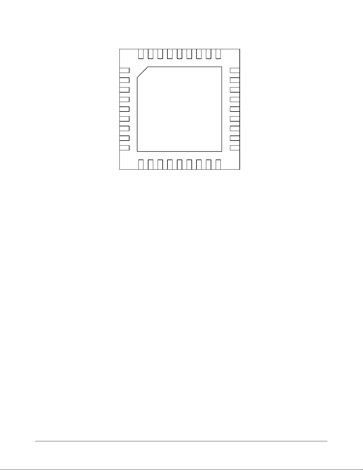
MARKING
DIAGRAM
1
NCP
36
1
QFN36
CASE 485CC
A = Assembly Location
WL = Wafer Lot
YY = Year
WW = Work Week
G = Pb−Free Package
ORDERING INFORMATION
See detailed ordering and shipping information in the package
dimensions section on page 35 of this data sheet.
81105
AWLYYWWG
© Semiconductor Components Industries, LLC, 2013
October, 2013 − Rev. 2
1 Publication Order Number:
NCP81105/D
Page 2
EN
VCC
VRHOT#
SDIO
ALERT#
SCLK
VR_RDY
ROSC
TSENSE
IMAX
INT_SEL
VBOOT
DGAIN
VRMP
1
2
VRMP
THERMAL
3
MONITOR
4
5
6
ENABLE
8
7
9
16
(VSP − VSN)
17
30
31
29
VR READY
IOUT
LOGIC
NCP81105
UVLO & EN
COMPARATORS
SVID
INTERFACE
& LOGIC
PS#
MUX
VRMP
ENABLE
DRVON
OCP
OVP
PS#
VRMP
PS#
NCP81105, NCP81105H
ENABLE
DATA
REGISTERS
ADC
OSCILLATOR
& RAMP
GENERATORS
VSP
DAC
DAC
FEED−
FORWARD
ENABLE
COMP
PWM
GENERATORS
PWM2
PWM3
PWM1
DRVON
POWER
STATE
GATE
VSN
OVP
OVP
DAC
OVERCURRENT
COMPARATORS
OCP
Buffer
DRVON
OVP
CURRENT
SENSE
AMP
PS#
OCP
DIFF
AMP
_
DAC
ERROR
AMP
OVERCURRENT
PROGRAMMING
_
+
ZERO
CURRENT
DETECTION
1.3V
CSREF
VSP
VSN
CSCOMP
SCALING
_
+
1.3V
CURRENT
MONITOR
IOUT
OVP
CURRENT
BALANCE
AMPLIFIERS
I2
I3
I1
MAX
OVP
36
35
34
33
32
28
27
26
25
24
23
22
21
20
19
18
15
11
14
13
12
10
VSP
VSN
DIFFOUT
FB
COMP
IOUT
ILIM
CSCOMP
CSSUM
CSREF
CSN2
CSP2
CSN3
CSP3
CSN1
CSP1
DRVON
SMOD
PWM1
PWM3
PWM2
OD#
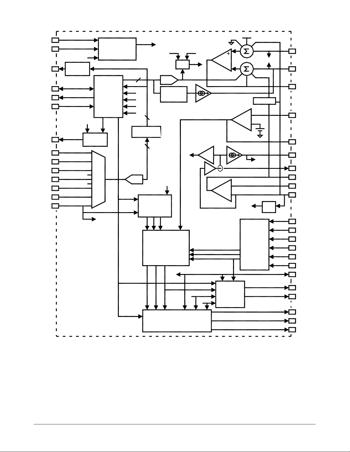
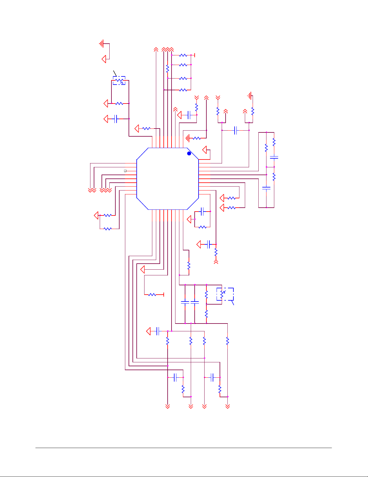
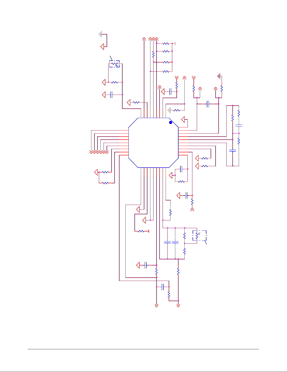
Figure 1. Block Diagram
http://onsemi.com
2
Page 3
EN
VCC
VRHOT#
SDIO
ALERT#
SCLK
ROSC
VR_RDY
TSENSE
NCP81105, NCP81105H
VSP
VSN
DIFFOUTFBCOMP
36
35
34
33
1
2
3
4
5
6
7
8
9
10
TAB: GROUND
111
12
NCP81105
13
DGAIN
VBOOT
VRMP
IOUT
32
31
30
29
28
27
ILIM
26
CSCOMP
25
CSSUM
24
CSREF
23
CSN2
22
CSP2
21
CSN3
20
CSP3
19
CSN1
14
15
16
17
18
OD#
SMOD
PWM2
PWM3
PWM1
DRVON
Figure 2. Pin Connections
(Top View)
IMAX
CSP1
INT_SEL
http://onsemi.com
3
Page 4

NCP81105, NCP81105H
PIN LIST AND DESCRIPTION
Pin
No.
1 EN Logic input. Logic high enables the NCP81105 and logic low disables it.
2 VCC Power for the internal control circuits. A decoupling capacitor must be connected from this pin to ground.
3 VR_HOT# Open drain (logic level) output for over−temperature reporting. Low indicates high temp.
4 SDIO Bidirectional Serial VID data interface.
5 ALERT# Open drain Serial VID ALERT# output.
6 SCLK Serial VID clock input.
7 ROSC This pin outputs a constant current. A resistance from this pin to ground programs the switching fre-
8 VR_RDY Open drain output. High indicates that the NCP81105 is regulating the output.
9 TSENSE Temperature sense input.
10 OD# Phase Disabling Output, tied to the Enable, SMOD or ZCD_EN# pin of phases 2 and 3 DrMOS. Except
11 SMOD Phase 1 Zero Cross Detection (ZCD) disable output. In PS2 & PS3, SMOD pulls LOW when phase 1
12 PWM2 PWM output to Phase 2 DrMOS
13 PWM3 PWM output to Phase 3 DrMOS
14 PWM1 PWM output to Phase 1 DrMOS
15 DRVON Enable output for DrMOS
16 IMAX During startup, a resistor from this pin to ground programs ICC_MAX.
17 INT_SEL During startup, a resistor from this pin to ground programs the low frequency compensator pole of the
18 CSP1 Positive input to phase 1 current sense amplifier for balancing phase currents
19 CSN1 Negative input to phase 1 current sense amplifier
20 CSP3 Positive input to phase 3 current sense amplifier for balancing phase currents
21 CSN3 Negative input to phase 3 current sense amplifier
22 CSP2 Positive input to phase 2 current sense amplifier for balancing phase currents
23 CSN2 Negative input to phase 2 current balance sense amplifier
24 CSREF Non−inverting input for the total output current sense amplifier. Also, the absolute OVP input.
25 CSSUM Inverting input of total output current sense amplifier.
26 CSCOMP Output of total output current sense amplifier.
27 ILIM Input to program the over−current shutdown threshold.
28 IOUT Total current monitor output. A resistor from this pin to ground calibrates SVID output current reporting.
29 VRMP VDC applied to this pin provides feed−forward compensation for the pulsewidth modulator. The current
30 VBOOT During startup, a resistor from this pin to ground programs the BOOT voltage
31 DGAIN During startup, a resistor from this pin to ground programs the scaling of the output Droop with respect to
32 COMP Output of the error amplifier.
33 FB Error amplifier voltage feedback input.
34 DIFFOUT Output of the differential remote sense amplifier.
35 VSN Inverting input to the differential remote sense amplifier (VSS sense).
36 VSP Non−inverting input to the differential remote sense amplifier (VCC sense).
37 GND Power supply return (QFN Flag)
Symbol Description
quency.
in PS0 mode, this output pulls low to disable the DrMOS if connected to an enable input. If connected to
a DrMOS SMOD or ZCD_EN# input, both HS & LS FETs are held off since PWM2 & PWM3 are also low.
Actively pulls high in PS0 mode.
inductor current is negative to perform (or allow the DrMOS ZCD function to perform) diode emulation,
and pulls HIGH when phase 1 inductor current is positive. In PS0 & PS1, SMOD stays high to force the
phase 1 DrMOS into Continuous Conduction.
NCP81105 voltage control feedback loop.
into this pin controls the slope of PWM ramp. A low voltage on this pin will inhibit NCP81105 startup.
the total output current signal produced between CSCOMP and CSREF.
http://onsemi.com
4
Page 5
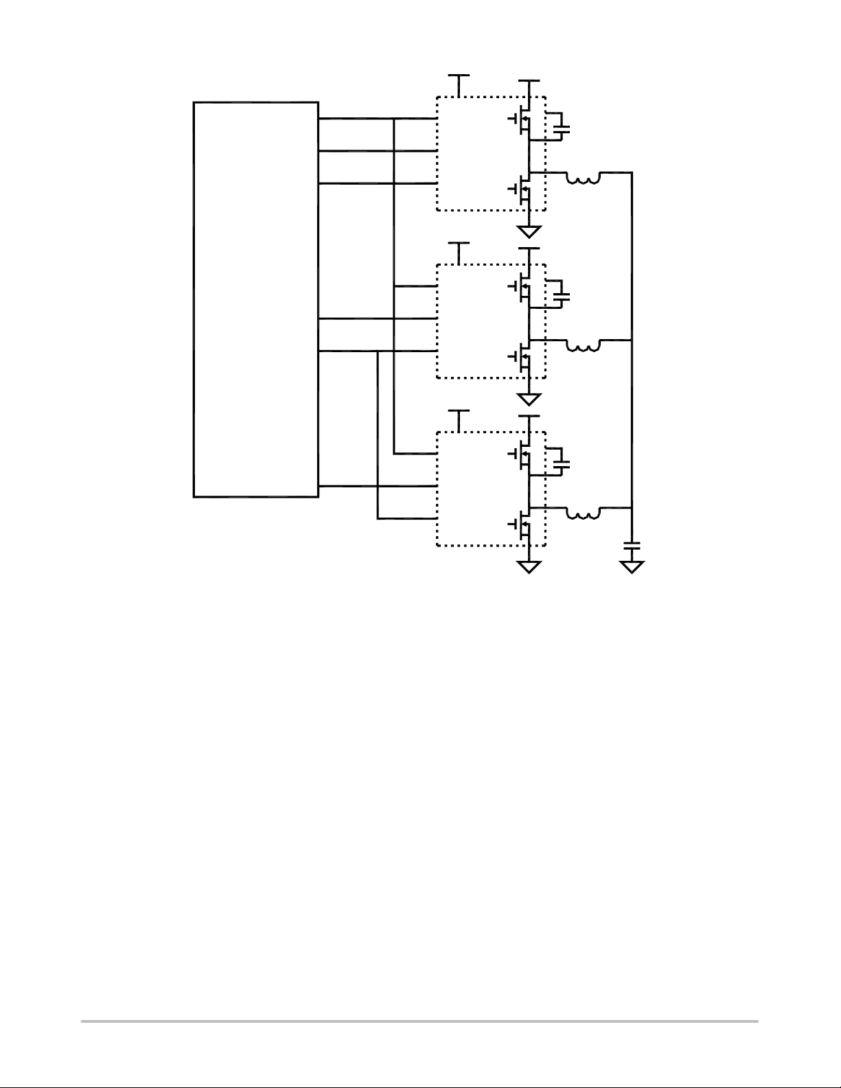
NCP81105, NCP81105H
DRVON
PWM1
SMOD
NCP81105
PWM2
PWM3
OD#
VCIN
EN
DRMOS
PWM
SMOD
VCIN
EN
DRMOS
PWM
SMOD
VCIN
EN
DRMOS
PWM
SMOD
VIN
BOOT
CB1
PHASE
VSWH
VIN
BOOT
CB2
PHASE
VSWH
VIN
BOOT
CB3
PHASE
VSWH
COUT
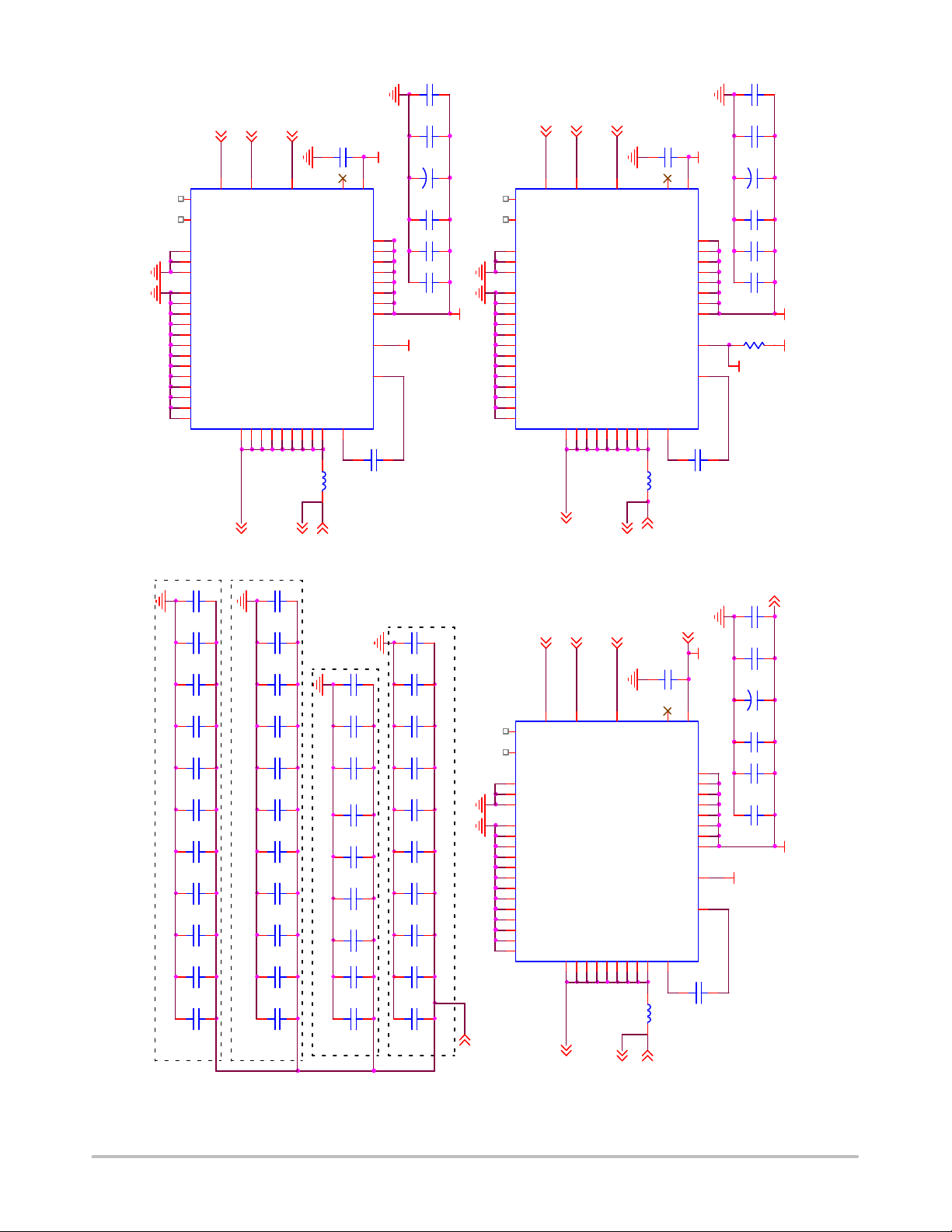
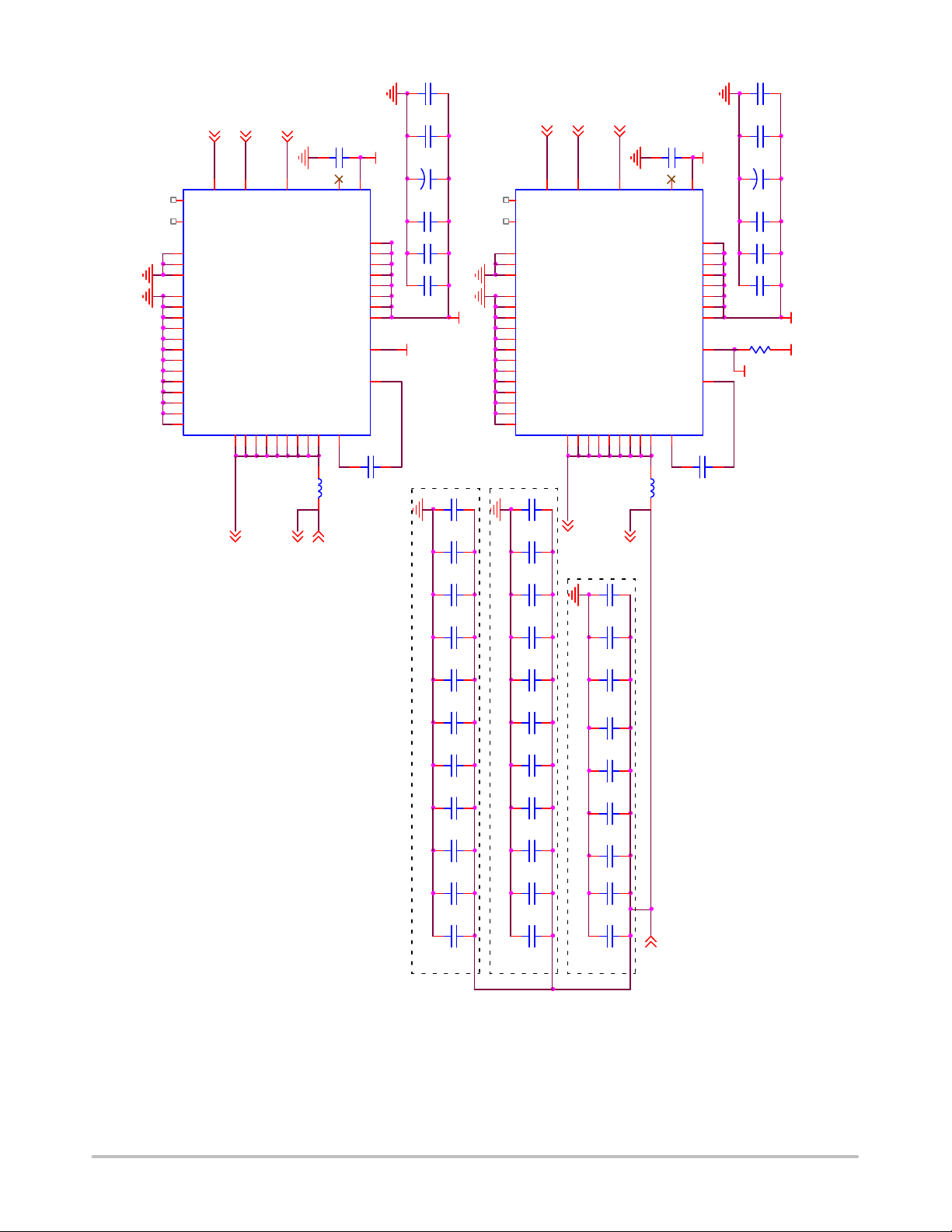
Figure 3. Three Phase Application Diagram
http://onsemi.com
5
Page 6
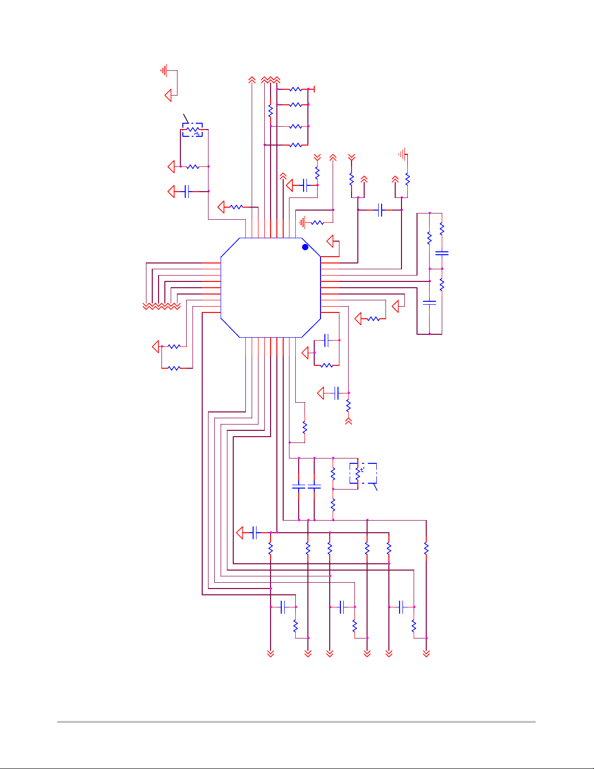
close to L1
OD#
PWM2
PWM3
SMOD
place
1nF
DRVON
PWM1
R25
75.0K
RT12
220K
11.0K
R31
C81
INT_SEL
IMAX
NCP81105, NCP81105H
VR_RDY
ALERT
SCLK
SDIO
R162
130
R78
R155
130
43.2
TSENSE
10
OD#
11
SMOD
12
PWM2
13
PWM3
14
PWM1
15
DRVON
16
IMAX
17
INT_SEL
18
CSP1
VR_RDY
R154
80.6K
TSENSE9VRHOT#
VR_RDY8VCC2EN
ROSC
CSN3
CSN1
CSP3
20
19
SCLK
ALERT_VR
SDIO
ROSC
5
4
7
SCLK6ALERT#
SDIO
NCP81105
CSREF
CSN2
CSP2
22
24
21
23
R157
75.0
R156
VR_HOT
54.9
1uF
VCC
VR_HOT
3
1
DIFFOUT
U1
DGAIN
VBOOT
CSCOMP
CSSUM
ILIM
25
27
26
C79
EPAD
COMP
VRMP
IOUT
V_1P05_VCCP
ENABLE
V5S
4.99
ENABLE
R71
R161
1.0K
37
36
VSP
35
VSN
34
33
FB
32
31
30
29
28
0.15uF
C61
VCCU
IMON
VRMP
VCC_SENSE
R48 100
1nF
VSP
69.8K
VSS_SENSE
VSENSE
C51
VBOOT
R19
R34 100
VSN
DGAIN
DIFFOUT
R37 1.00K
FB
10pF
C57
COMPDIFFOUT
R50
37.4
C56
270pF
R43
4.75K
R26
51.1K
790kHz switching frequency
95A maximum output current
114A current limit
1.5mOhm loadline
1.7V boot voltage
CSP2
CSN1
CSN2
CSP3
CSP1
CSN3
10nF
C66
10.0
CSREF
R185
22nF
C80
CSCOMP
ILIM
17.4K
68pF
CSSUM
10.0K
R9
C156
100K
23.7K
R18
C155
680pF
R140
R38
0.01uF
73.2K
165K
10.0
1.0K
C82
RCS11
RCS12
R8
22nF
C83
R40
VDC
10.0K
RT11
220K
close
to L1
R139
100K
R10
place
R12
10.0
22nF
C85
100K
10.0K
R138
R27
CSN1
CSPP1
CSN3
CSPP3
CSN2
Figure 4. Three Phase Control Circuit Application
http://onsemi.com
6
CSPP2
Page 7
PWM3
DRVON
OD#
NCP81105, NCP81105H
10uF
CA3
PWM1
DRVON
SMOD
10uF
CA1
6
36
41
5
37
16
17
18
19
20
21
22
23
24
25
26
27
28
LOCATE IN CENTER OF SOCKET rPGA989 CAVITY (PRIMARY SIDE)
GH
GL
CGND
CGND
CGND
PGND
PGND
PGND
PGND
PGND
PGND
PGND
PGND
PGND
PGND
PGND
PGND
PGND
22uF
22uF
22uF
22uF
22uF
22uF
22uF
22uF
22uF
22uF
22uF
C212
C213
C226
C227
C176
C177
C183
C184
C273
C271
C272
40
PWM
39
DISB#
VSWH31VSWH32VSWH33VSWH34VSWH
VSWH29VSWH
30
CSPP3
10uF
LOCATE IN CENTER OF SOCKET rPGA989 CAVITY (BOTTOM SIDE)
10uF
10uF
10uF
10uF
10uF
10uF
10uF
10uF
10uF
10uF
C29
1uF
ZCD_EN#1VCIN
NCP5338
U4
THWN
BOOT
PHASE
VSWH
VSWH
15
35
43
MPCG0740LR12
0.7mOhm
SW3
120nH
L3
CSNN3
VCCU
C214
C41
C48
LOCATE BETWEEN L1 & L2 (PRIMARY SIDE)
C49
C215
C216
C217
C204
C205
C206
C207
VIN
VIN
VIN
VIN
VIN
VIN
VIN
VIN
7
C52
22uF
C67
22uF
C68
22uF
C78
22uF
C84
22uF
C98
22uF
C99
22uF
C100
22uF
C196
DNP
2NC3
0.22uF
CB3
10uF
V5S
12
+
C3
33uF
C31
1uF
42
14
13
12
11
10
9
8
38
4
C28
C32
1uF
C9
1uF
VDC
THWN
Capacitor:
26 X 22uF(0805)
+ 11 X 10uF(0805)
C42
22uF
C43
DNP
C45
DNP
LOCATE BETWEEN L2 & L3 (PRIMARY SIDE)
C46
22uF
C95
22uF
C97
DNP
C189
22uF
C190
22uF
C210
22uF
C222
22uF
VCCU
39
40
DISB#
PWM
6
GH
36
GL
41
CGND
5
CGND
37
CGND
16
PGND
17
PGND
18
PGND
19
PGND
20
PGND
21
PGND
22
PGND
23
PGND
24
PGND
25
PGND
26
27
28
PGND
PGND
PGND
VSWH29VSWH
ZCD_EN#1VCIN
VSWH31VSWH32VSWH33VSWH34VSWH
30
Total VCORE Output
CSPP1
DRVON
PWM2
40
PWM
6
GH
36
GL
41
CGND
5
CGND
37
CGND
16
PGND
17
PGND
18
PGND
19
PGND
20
PGND
21
PGND
22
PGND
23
PGND
24
PGND
25
PGND
26
27
28
PGND
PGND
PGND
VSWH29VSWH
OD#
39
DISB#
ZCD_EN#1VCIN
VSWH31VSWH32VSWH33VSWH34VSWH
30
SW2SW1
CSPP2
NCP5338
U2
VSWH
35
43
0.7mOhm
120nH
CSN1
NCP5338
U3
VSWH
35
43
0.7mOhm
120nH
CSNN2
1uF
C5
2NC3
VIN
VIN
VIN
VIN
VIN
VIN
VIN
VIN
THWN
BOOT
PHASE
VSWH
7
15
MPCG0740LR12
0.22uF
L1
VCCU
V5S
C44
1uF
2NC3
VIN
VIN
VIN
VIN
VIN
VIN
VIN
VIN
THWN
BOOT
PHASE
VSWH
7
15
MPCG0740LR12
0.22uF
L2
VCCU
C4
42
14
13
12
11
10
9
8
38
4
V5SV5S
42
14
13
12
11
10
9
8
38
4
C37
10uF
33uF
1uF
1uF
1uF
1k
THWN
10uF
10uF
33uF
1uF
1uF
1uF
THWN
CB1
+
C1
C25
C26
C20
R121
CA2
CB2
+
C2
C27
C30
C36
12
V5S
VDC
12
VDCVDC
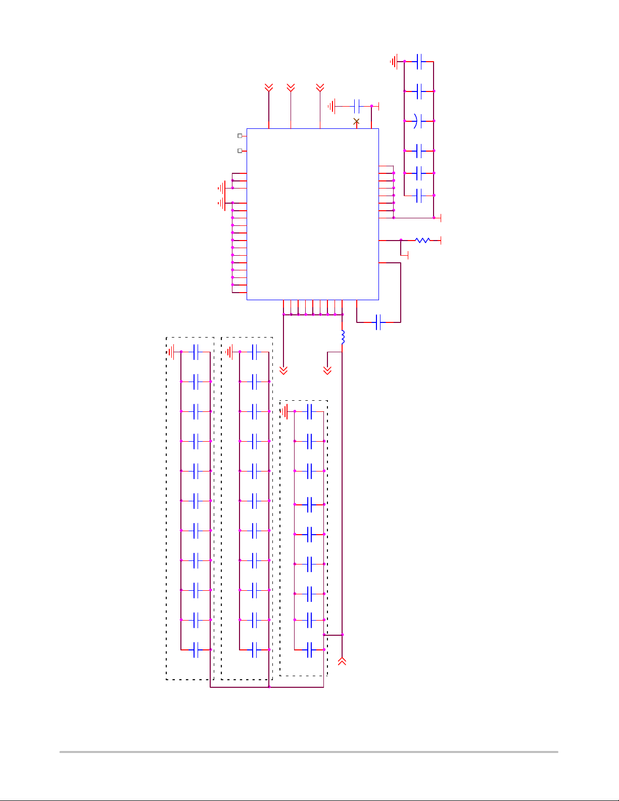
Figure 5. Three Phase Power Stage Circuit
http://onsemi.com
7
Page 8
OD#
SMOD
PWM3
place
close to L1
RT12
220K
11.0K
R31
1nF
C81
TSENSE
10
11
12
13
14
15
16
17
INT_SEL
IMAX
18
DRVON
PWM1
R25
43.2K
NCP81105, NCP81105H
VR_RDY
ALERT
SCLK
VR_RDY
R154
80.6K
TSENSE9VRHOT#
VR_RDY8VCC2EN
ROSC
OD#
SMOD
PWM2
PWM3
PWM1
DRVON
IMAX
INT_SEL
CSP1
CSN1
CSP3
19
CSN3
20
SDIO
R78
43.2
VR_HOT
SCLK
ALERT_VR
SDIO
ROSC
5
4
7
SCLK6ALERT#
SDIO
NCP81105
CSSUM
CSREF
CSN2
CSP2
21
23
22
24
R162
R155
54.9
VR_HOT
3
U1
CSCOMP
25
130
130
R157
75.0
R156
C79
1uF
VCC
1
EPAD
VSN
DIFFOUT
COMP
DGAIN
VBOOT
VRMP
IOUT
ILIM
27
26
V_1P05_VCCP
V5S
4.99
R71
R161
1.0K
37
36
VSP
35
34
33
FB
32
31
30
29
28
0.15uF
ENABLE
ENABLE
C61
IMON
VCCU
VCC_SENSE
R48 100
VSP
69.8K
24.9K
VRMP
VSS_SENSE
VSENSE
C51
1nF
VBOOT
R19
R16
R34 100
VSN
DGAIN
DIFFOUT
R37 1.00K
FB
10pF
C57
COMPDIFFOUT
R50
37.4
C56
270pF
R43
4.75K
R26
51.1K
790kHz switching frequency
55A maximum output current
66A current limit
1.5mOhm loadline
1.7V boot voltage
CSN2
R128
1K
CSN1
CSP3
CSP1
CSN3
10nF
C66
V5S
10.0
CSREF
R185
22nF
C80
CSCOMP
ILIM
20.0k
68pF
CSSUM
10.0K
R9
R18
C156
680pF
49.9k
23.7K
C155
R140
R38
0.01uF
73.2K
165K
10.0
1.0K
C82
RCS11
RCS12
R8
22nF
C83
R40
VDC
10.0K
RT11
220K
close
to L1
R139
49.9k
R10
place
CSN1
CSPP1
CSN3
CSPP3
Figure 6. Two Phase Control Circuit Application
http://onsemi.com
8
Page 9
PWM3
DRVON
OD#
NCP81105, NCP81105H
10uF
CA3
PWM1
DRVON
SMOD
10uF
CA1
C29
1uF
39
40
DISB#
PWM
6
GH
36
GL
41
CGND
5
CGND
37
CGND
16
PGND
17
PGND
18
PGND
19
PGND
20
PGND
21
PGND
22
PGND
23
PGND
24
PGND
25
PGND
26
27
28
PGND
PGND
PGND
VSWH29VSWH
CSPP3
ZCD_EN#1VCIN
NCP5338
U4
VSWH31VSWH32VSWH33VSWH34VSWH
30
SW3
VSWH
35
0.7mOhm
120nH
CSNN3
VSWH
15
43
MPCG0740LR12
VCCU
VIN
VIN
VIN
VIN
VIN
VIN
VIN
VIN
THWN
BOOT
PHASE
7
0.22uF
L3
V5S
2NC3
42
14
13
12
11
10
9
8
38
4
C28
10uF
33uF
1uF
1uF
1uF
THWN
LOCATE IN CENTER OF SOCKET rPGA989 CAVITY (PRIMARY SIDE)
CB3
+
C3
C31
C32
C9
12
C212
22uF
C213
22uF
VDC
PWM
6
GH
36
GL
41
CGND
5
CGND
37
CGND
16
PGND
17
PGND
18
PGND
19
PGND
20
PGND
21
PGND
22
PGND
23
PGND
24
PGND
25
PGND
26
PGND
27
PGND
28
PGND
C214
10uF
LOCATE IN CENTER OF SOCKET rPGA989 CAVITY (BOTTOM SIDE)
C41
10uF
40
DISB#
VSWH29VSWH
CSPP1
39
VSWH31VSWH32VSWH33VSWH34VSWH
30
1uF
C5
ZCD_EN#1VCIN
VIN
VIN
VIN
VIN
U2
THWN
BOOT
PHASE
VSWH
VSWH
15
35
43
7
MPCG0740LR12
120nH
L1
VIN
VIN
VIN
VIN
NCP5338
SW1
CSN1
0.7mOhm
V5S
2NC3
42
14
13
12
11
10
9
8
38
4
0.22uF
C4
CB1
10uF
+
C1
33uF
1uF
1uF
1uF
R121
1k
THWN
12
C25
C26
C20
VDC
V5S
C226
22uF
C227
22uF
C176
22uF
C177
22uF
C183
22uF
C184
22uF
C273
22uF
C271
22uF
C272
22uF
C48
10uF
C49
10uF
C215
10uF
C216
10uF
C217
10uF
C204
10uF
C205
10uF
C206
10uF
C207
10uF
LOCATE BETWEEN L1 & L2 (PRIMARY SIDE)
Figure 7. Two Phase Power Stage Circuit
C52
22uF
C67
22uF
C68
22uF
C78
22uF
C84
22uF
C98
22uF
C99
22uF
C100
22uF
C196
22Uf
Total VCORE Output
Capacitor:
20 X 22uF(0805)
+ 11 X 10uF(0805)
VCCU
http://onsemi.com
9
Page 10
close to L1
PWM1
OD#
PWM2
PWM3
SMOD
25.5K
NCP81105, NCP81105H
VR_RDY
ALERT
SCLK
place
220K
11.0K
1nF
DRVON
IMAX
R25
RT12
R31
C81
INT_SEL
TSENSE
10
OD#
11
SMOD
12
PWM2
13
PWM3
14
PWM1
15
DRVON
16
IMAX
17
INT_SEL
18
CSP1
R154
80.6K
TSENSE9VRHOT#
CSN1
R78
43.2
VR_RDY
SCLK
ALERT_VR
ROSC
5
7
SCLK6ALERT#
VR_RDY8VCC2EN
ROSC
CSN3
CSN2
CSP3
CSP2
21
19
23
20
22
SDIO
R162
R155
R157
R156
VR_HOT
54.9
SDIO
VR_HOT
3
4
SDIO
NCP81105
U1
CSCOMP
CSSUM
CSREF
24
25
130
130
75.0
C79
1uF
VCC
1.0K
1
EPAD
VSP
VSN
DIFFOUT
COMP
DGAIN
VBOOT
VRMP
IOUT
ILIM
27
26
V_1P05_VCCP
ENABLE
V5S
4.99
ENABLE
R71
R161
37
36
35
34
33
FB
32
31
30
29
28
0.15uF
C61
IMON
VCCU
VCC_SENSE
R48 100
VSP
69.8K
24.9K
VRMP
VSS_SENSE
VSENSE
C51
1nF
VBOOT
R19
R16
R34 100
VSN
DGAIN
DIFFOUT
R37 1.00K
FB
10pF
C57
COMPDIFFOUT
R50
37.4
C56
270pF
R43
4.75K
R26
51.1K
CSP1
790kHz switching frequency
32A maximum output current
39A current limit
2.0mOhm loadline
1.7V boot voltage
CSN3
R128
1K
CSN1
10nF
C66
V5S
10.0
CSREF
CSSUM
R185
22nF
CSN1
CSCOMP
ILIM
8.87K
68pF
C156
C80
10.0K
R9
23.7K
R18
C155
680pF
75.0K
CSPP1
R38
0.01uF
73.2K
165K
R140
1.0K
C82
RCS11
RCS12
R40
VDC
RT11
220K
close
to L1
place
Figure 8. Single Phase Control Circuit Application
http://onsemi.com
10
Page 11
NCP81105, NCP81105H
DRVON
PWM1
40
DISB#
PWM
6
GH
36
GL
41
CGND
5
CGND
37
CGND
16
PGND
17
PGND
18
PGND
19
PGND
20
PGND
21
PGND
22
PGND
23
PGND
24
PGND
25
PGND
26
27
28
PGND
PGND
PGND
VSWH29VSWH
SMOD
39
ZCD_EN#1VCIN
NCP5338
VSWH31VSWH32VSWH33VSWH34VSWH
30
SW1
VSWH
35
0.7mOhm
1uF
U2
VSWH
15
43
120nH
C5
VIN
VIN
VIN
VIN
VIN
VIN
VIN
VIN
THWN
BOOT
PHASE
7
V5S
2NC3
42
14
13
12
11
10
9
8
38
4
MPCG0740LR12
0.22uF
C4
L1
CA1
10uF
CB1
10uF
+
C1
33uF
1uF
1uF
1uF
1k
THWN
12
C25
C26
C20
VDC
V5S
R121
LOCATE IN CENTER OF SOCKET rPGA989 CAVITY (PRIMARY SIDE)
C212
22uF
C213
22uF
C226
22uF
C227
22uF
C176
22uF
C177
22uF
C183
22uF
C184
22uF
C273
22uF
C271
22uF
C214
10uF
LOCATE IN CENTER OF SOCKET rPGA989 CAVITY (BOTTOM SIDE)
C41
10uF
C48
10uF
C49
10uF
C215
10uF
C216
10uF
C217
10uF
C204
10uF
C205
10uF
C206
10uF
CSPP1
LOCATE NEAR L1 (PRIMARY SIDE)
C52
DNP
C67
DNP
C68
DNP
C78
22uF
C84
22uF
C98
22uF
C99
22uF
C100
22uF
CSN1
Total VCORE Output
Capacitor:
16 X 22uF(0805)
+ 11 X 10uF(0805)
C196
C272
22uF
10uF
C207
DNP
VCCU
Figure 9. Single Phase Power Stage Circuit
http://onsemi.com
11
Page 12

NCP81105, NCP81105H
ABSOLUTE MAXIMUM RATINGS
ELECTRICAL INFORMATION − all signals referenced to GND unless noted otherwise.
Pin Symbol V
MAX
COMP, CSCOMP, DIFFOUT VCC + 0.3 V −0.3 V 3 mA 3 mA
VSN GND + 300 mV GND − 300 mV
VR_RDY VCC + 0.3 V −0.3 V N/A 5 mA
VCC 6.5 V −0.3 V N/A N/A
VRMP +25 V −0.3 V
VR_HOT#, SDIO & ALERT# VCC + 0.3 V −0.3 V 0 mA 30 mA
OD#, SMOD, PWM1, PWM2,
VCC + 0.3 V −0.3 V 5 mA 5 mA
PWM3 & DRVON
All Other Pins VCC + 0.3 V −0.3 V
Stresses exceeding Maximum Ratings may damage the device. Maximum Ratings are stress ratings only. Functional operation above the
Recommended Operating Conditions is not implied. Extended exposure to stresses above the Recommended Operating Conditions may affect
device reliability.
THERMAL INFORMATION
Description Symbol Typ Unit
Thermal Characteristic
QFN36 Package (Notes 1 and 2)
Operating Junction Temperature Range* T
Operating Ambient Temperature Range −10 to 100
Maximum Storage Temperature Range T
Moisture Sensitivity Level MSL 1
*The maximum package power dissipation must be observed.
1. JESD 51−5 (1S2P Direct−Attach Method) with 0 LFM
2. JESD 51−7 (1S2P Direct−Attach Method) with 0 LFM
V
MIN
R
q
JA
J
I
SOURCE
68
−10 to 125
I
SINK
_C/W
_C
_C
STG
−40 to +150
_C
ELECTRICAL CHARACTERISTICS (V
for the temperature range −10°C ≤ T
Parameter
≤ 100°C unless noted otherwise, and are guaranteed by test, design or statistical correlation.
A
= 5.0 V, VEN = 2.0 V, C
CC
= 0.1 mF unless specified otherwise) Min/Max values are valid
VCC
Symbol Conditions Min Typ Max Unit
VCC INPUT
Supply Voltage Range
4.75 5.25 V
EN = high; PS0, 1, 2 modes 23 29 mA
Quiescent Current
UVLO Threshold
EN = high; PS3 Mode 14 17.5 mA
EN = low 30
mA
VCC rising 4.5 V
VCC falling 4.0 V
UVLO Hysteresis 160 mV
VRMP (VIN monitor)
UVLO Threshold
VRMP falling 3.0 3.2 3.4 V
UVLO Hysteresis 600 800 mV
Leakage current PS0, PS1, PS2, PS3; V
Leakage current PS4, V
Leakage current VEN = 0 V, V
VRMP
VRMP
= 3.2 V 70
VRMP
mA
= 20 V 500 nA
= 20 V 500 nA
ENABLE INPUT
Enable High Input Leakage Current
External 1k pull−up to 3.3 V 1.0
mA
http://onsemi.com
12
Page 13

NCP81105, NCP81105H
ELECTRICAL CHARACTERISTICS (V
for the temperature range −10°C ≤ T
≤ 100°C unless noted otherwise, and are guaranteed by test, design or statistical correlation.
A
= 5.0 V, VEN = 2.0 V, C
CC
= 0.1 mF unless specified otherwise) Min/Max values are valid
VCC
Parameter UnitMaxTypMinConditionsSymbol
ENABLE INPUT
Upper Threshold
Lower Threshold V
Total Hysteresis V
Enable Delay Time
V
UPPER
LOWER
− V
UPPER
LOWER
Time from Enable transitioning HI to when
DRVON goes high.
0.8 V
0.3 V
300 mV
2.4 ms
SCLK, SDIO, ALERT#
SCLK Input Low Voltage
VILSCLK 0.45 V
SCLK Input High Voltage VIHSCLK 0.66 V
SDIO Input Low Voltage VILSDIO 0.42 V
SDIO Input High Voltage VIHSDIO 0.72 V
Hysteresis Voltage (SCLK, SDIO) VHYS 100 mV
Output High Voltage (SDIO, ALERT#) VOH External resistive pullup to 1.05 V 1.05 V
Output Low Voltage (SDIO, ALERT#) VOL Sinking 20 mA 100 mV
Buffer On Resistance (SDIO, ALERT#) RON Measured sinking 4 mA 5 13
Leakage Current Pin voltage between 0 and 1.05 V −100 100
W
mA
Pin Capacitance 4.0 pF
VR clock to data delay T
Setup time TSU
Hold time THLD
Time between SCLK rising edge and valid
CO
SDIO level
Time before SCLK falling (sampling) edge
that SDIO level must be valid
Time after SCLK falling edge that the
SDIO level remains valid
4 8.3 ns
7 ns
14 ns
VR12.5 & VR12.6 DAC
1.5 V ≤ DAC < 2.3 V, −10°C ≤ TA ≤ 85°C −0.5 0.5 %
System Voltage Accuracy
1.0 V ≤ DAC < 1.49 V, −10°C ≤ TA ≤ 85°C −8 8 mV
0.5 V ≤ DAC < 0.99 V, −10°C ≤ TA ≤ 85°C −10 10 mV
DAC SLEW RATES (NCP81105)
Soft Start Slew Rate
Slew Rate Slow Selectable Fraction of Fast Slew 3 − 24
Slew Rate Fast 48
SVID Register 2Ah = default 12
mV/ms
mV/ms
mV/ms
DAC SLEW RATES (NCP81105H)
Soft Start Slew Rate
Slew Rate Slow Selectable Fraction of Fast Slew 1 − 5
Slew Rate Fast 10
SVID Register 2Ah = default 2.5
mV/ms
mV/ms
mV/ms
DIFFERENTIAL SUMMING AMPLIFIER
V
VSP Input Leakage Current
VSN Bias Current −0.3 V ≤ V
DVID UP Feedforward Charge −0.3 V ≤ V
Charge per 5 mV DAC increment
= 1.3 V 0 15
VSP
≤ 0.3 V −1 1
VSN
VSN
≤ 0.5 V
6.8 pC
mA
mA
VSP Input Voltage Range −0.3 3.0 V
VSN Input Voltage Range −0.3 0.3 V
−3dB Bandwidth
CL = 20 pF to GND, RL = 10 kW to GND
10 MHz
DC gain − VSx to DIFFOUT VSP − VSN = 0.5 V to 2.3 V 1.0 V/V
http://onsemi.com
13
Page 14

NCP81105, NCP81105H
ELECTRICAL CHARACTERISTICS (V
for the temperature range −10°C ≤ T
≤ 100°C unless noted otherwise, and are guaranteed by test, design or statistical correlation.
A
= 5.0 V, VEN = 2.0 V, C
CC
= 0.1 mF unless specified otherwise) Min/Max values are valid
VCC
Parameter UnitMaxTypMinConditionsSymbol
DIFFERENTIAL SUMMING AMPLIFIER
Maximum Output Voltage
Minimum Output Voltage I
I
= 2 mA 3.0 V
SOURCE
= 2 mA 0.5 V
SINK
ERROR AMPLIFIER
Input Bias Current
Open Loop DC Gain
Open Loop Unity Gain Bandwidth
VFB = 1.3 V; Internal integrator active −25 25
CL = 20 pF to GND,
RL = 10 kW to GND
CL = 20 pF to GND,
RL = 10 kW to GND
80 dB
20 MHz
mA
DVin = 100 mV, G = −10 V/V,
Slew Rate
DVout = 1.5 V − 2.5 V,
20
V/ms
Load = 20 pF to GND + 10 kW to GND
Maximum Output Voltage I
Minimum Output Voltage I
= 2.0 mA 3.5 V
SOURCE
= 2.0 mA 1 V
SINK
VR_RDY (Power Good) OUTPUT
I
Output Low Saturation Voltage
Rise Time
Fall Time
Output Voltage at Power−up
1 kW external pull−up to 3.3 V,
1 kW external pull−up to 3.3 V,
VR_RDY pulled up to 5 V via 2 kW
Output Leakage Current When High VR_RDY = 5.0 V −1.0 1.0
VR_RDY Delay (rising) DAC = TARGET to VR_RDY high 5.5 6
VR_RDY Delay (falling) From OCP or OVP to VR_RDY low 5
= 4 mA 0.3 V
VR_RDY
C
C
TOT
TOT
= 45 pF
= 45 pF
100 ns
10 ns
1.0 V
mA
ms
ms
OUTPUT OVER VOLTAGE & UNDER VOLTAGE PROTECTION (OVP & UVP)
Absolute Over Voltage Threshold
During Soft−Start
2.8 2.9 3.0 V
Over Voltage Threshold Above DAC VSP rising 350 400 425 mV
Over Voltage Delay VSP rising to PWMx low 50 ns
Under Voltage Threshold Below DAC VSP falling 300 mV
Under−voltage Delay 5
ms
CURRENT BALANCE AMPLIFIERS
Input Bias Current (after phase
detection)
CSPx = CSNx = 1.7 V −50 50 nA
Common Mode Input Voltage Range CSPx = CSNx 0 2.3 V
Differential Mode Input Voltage Range CSNx = 1.7 V −100 100 mV
Closed loop Input Offset Voltage
Matching
CSPx = CSNx = 1.7 V,
Measured from the average offset
−1.5 1.5 mV
Amplifier Gain 0 V < CSPx−CSNx ≤ 0.1 V 5.7 6.0 6.3 V/V
Gain Matching 10 mV ≤ CSPx−CSNx ≤ 30 mV −3 3 %
−3 dB Bandwidth 8 MHz
1 & 2 PHASE DETECTION
CSN Pin Resistance to Ground
During phase detection only 50
kW
CSN Pin Threshold Voltage 4.5 V
Phase Detect Timer
Time from Enable transitioning HI to
removal of phase detect resistance
3.5 ms
http://onsemi.com
14
Page 15

NCP81105, NCP81105H
ELECTRICAL CHARACTERISTICS (V
for the temperature range −10°C ≤ T
≤ 100°C unless noted otherwise, and are guaranteed by test, design or statistical correlation.
A
= 5.0 V, VEN = 2.0 V, C
CC
= 0.1 mF unless specified otherwise) Min/Max values are valid
VCC
Parameter UnitMaxTypMinConditionsSymbol
CURRENT SUMMING AMPLIFIER
Offset Voltage
VOS V
= 1.0 V −300 300
CSREF
mV
CSSUM Input Bias Current CSSUM = CSREF = 1 V −7.5 7.5 nA
CSREF Input Bias Current CSSUM = CSREF = 1 V 0 4.25
mA
Open Loop Gain 80 dB
Current Sense Unity Gain Bandwidth
CL = 20 pF to GND, RL = 10 kW to GND
10 MHz
Max CSCOMP Output Voltage Isource = 2 mA 3.5 V
Minimum CSCOMP Output Voltage
Isink = 500 mA
Isink = 25 mA
7.0 30 mV
100 mV
IOUT OUTPUT
Maximum Output Voltage
R
IOUT
= 5 kW
2.0 V
Input Referred Offset Voltage ILIM minus CSREF −1.9 1.9 mV
Output Source Current
Current Gain AI
DIMON Full Scale Voltage V
IOUT
DIFS
ILIM sink current = 80 mA
(IOUT
R
ILIM
CURRENT
= 20 kW; R
V
CSREF
) / (ILIM
IOUT
= 1.7 V
CURRENT
= 5.0 kW;
);
700
mA
9.5 10 10.5 A/A
2.0 V
OVERCURRENT PROTECTION (ILIM pin)
3 & 2−phase PS0 Threshold Current,
mA
1−phase all−PS Threshold Current
Delayed shutdown
Immediate shutdown
3−phase, non−PS0 Threshold Current
Delayed shutdown
Immediate shutdown
2−phase, non−PS0 Threshold Current
Delayed shutdown
Immediate shutdown
Time for Delayed Shutdown 55
I
DS
I
IS
9.0
13.5
10
15
11.0
16.5
mA
I
DS
I
IS
PS1, 2 or 3 mode (1−phase active)
PS1, 2 or 3 mode (1−phase active)
4
6
mA
I
DS
I
IS
PS1, 2 or 3 mode (1−phase active)
PS1, 2 or 3 mode (1−phase active)
6.7
10
ms
OSCILLATOR
Maximum Switching Frequency
See Precision Oscillator description 1425 kHz
Minimum Switching Frequency See Precision Oscillator description 275 kHz
Switching Frequency Tolerance
PS0 mode; RROSC = 110 kW
ROSC Pin Output Current V
= GND 9.5 10 10.5
ROSC
925 1025 1125 kHz
mA
MODULATORS (PWM Comparators)
Minimum Pulse Width
0% Duty Cycle
COMP voltage when the PWM outputs
remain Lo (Dual−edge modulation only)
20 ns
1.3 V
COMP voltage when the PWM outputs
100% Duty Cycle
remain HI, VRMP = 12.0 V; (Dual−edge
2.5 V
modulation only)
PWM Phase Angle Error
Between adjacent phases, 3−phase
operation
−20 20 deg
Ramp Feed−forward Voltage range VRMP pin voltage 5 20 V
PWM OUTPUTS (PWM1/2/3)
Output High Voltage
Output Low Voltage
Sourcing 500 mA
Sinking 500 mA
VCC −
0.2
V
0.7 V
http://onsemi.com
15
Page 16

NCP81105, NCP81105H
ELECTRICAL CHARACTERISTICS (V
for the temperature range −10°C ≤ T
≤ 100°C unless noted otherwise, and are guaranteed by test, design or statistical correlation.
A
= 5.0 V, VEN = 2.0 V, C
CC
= 0.1 mF unless specified otherwise) Min/Max values are valid
VCC
Parameter UnitMaxTypMinConditionsSymbol
PWM OUTPUTS (PWM1/2/3)
Rise and Fall Times
CL (PCB) = 50 pF, measured between
10% & 90% of V
CC
10 ns
DRVON OUTPUT
Output High Voltage
Output Low Voltage
Rise Time
Fall Time
CL (PCB) = 20 pF, DVo = 10% to 90%
CL (PCB) = 20 pF, DVo = 90% to 10%
Sourcing 500 mA
Sinking 500 mA
PWM delay time Time from DRVON high to first PWM 11 0 120
Internal Pull Down Resistance EN = Low 70
3.0 V
0.1 V
150 ns
5 ns
ms
kW
OD# OUTPUT
Output High Voltage
Output Low Voltage
PS0 Delay
Rise/Fall Time
Entering PS0; from fall of the earlier of
CL (PCB) = 20 pF, DVo = 10% to 90%
Sourcing 500 mA
Sinking 500 mA
PWM2 or PWM3 to OD# rising
Internal Pull Down Resistance EN = Low 70
3.0 V
0.1 V
15 ns
10 ns
kW
SMOD OUTPUT
Output High Voltage
Output Low Voltage
Sourcing 500 mA
Sinking 500 mA
3.0 V
0.1 V
PS2/3 Delay PS2&3; PWM1 rising to SMOD rising 10 50 ns
Rise/Fall Time
CL (PCB) = 20 pF, DVo = 10% to 90%
Internal Pull Down Resistance EN = Low 70
10 ns
kW
VR_HOT# OUTPUT
Output Low Voltage
I
_VRHOT#
Output Leakage Current High Impedance State, V
= −4 mA 0.3 V
= 3.3 V −1.0 1.0
VRHOT#
mA
TSENSE INPUT
Alert# Assert Threshold
TA = 85°C 458 mV
Alert# De−assert Threshold TA = 85°C 476 mV
VRHOT# Assert Threshold TA = 85°C 437 mV
VRHOT# De−assert Threshold TA = 85°C 457 mV
TSENSE Bias Current V
= 0.4 V, TA = 85°C 57.7 60 62.7
TSENSE
mA
VBOOT PIN
Sensing Current
VVBOOT = GND 10
mA
IMAX PIN
Sensing Current
IMAX Full Scale Voltage V
I
IMAX
IMAXFS
VIMAX = GND 9.5 10 10.5
2.0 V
mA
INT_SEL PIN
Sensing Current
VINT_SEL = GND 10
mA
DGAIN PIN
Sensing Current
VDGAIN = GND 10
mA
ADC
Input Voltage Range
0 2 V
http://onsemi.com
16
Page 17

NCP81105, NCP81105H
ELECTRICAL CHARACTERISTICS (V
for the temperature range −10°C ≤ T
Parameter UnitMaxTypMinConditionsSymbol
ADC
Total Unadjusted Error (TUE)
Differential Nonlinearity (DNL) 8−bit 1 LSB
Power Supply Sensitivity ±1 %
Conversion Time 10
Time to cycle through all inputs 250
≤ 100°C unless noted otherwise, and are guaranteed by test, design or statistical correlation.
A
= 5.0 V, VEN = 2.0 V, C
CC
= 0.1 mF unless specified otherwise) Min/Max values are valid
VCC
−1 +1 %
ms
ms
http://onsemi.com
17
Page 18

NCP81105, NCP81105H
VR12.5 & VR12.6 VID TABLE
Voltage
VID7 VID6 VID5 VID4 VID3 VID2 VID1 VID0
0 0 0 0 0 0 0 0 OFF 00 0 0 1 1 1 1 1 0 1.11 3E
0 0 0 0 0 0 0 1 0.50 01 0 0 1 1 1 1 1 1 1.12 3F
0 0 0 0 0 0 1 0 0.51 02 0 1 0 0 0 0 0 0 1.13 40
0 0 0 0 0 0 1 1 0.52 03 0 1 0 0 0 0 0 1 1.14 41
0 0 0 0 0 1 0 0 0.53 04 0 1 0 0 0 0 1 0 1.15 42
0 0 0 0 0 1 0 1 0.54 05 0 1 0 0 0 0 1 1 1.16 43
0 0 0 0 0 1 1 0 0.55 06 0 1 0 0 0 1 0 0 1.17 44
0 0 0 0 0 1 1 1 0.56 07 0 1 0 0 0 1 0 1 1.18 45
0 0 0 0 1 0 0 0 0.57 08 0 1 0 0 0 1 1 0 1.19 46
0 0 0 0 1 0 0 1 0.58 09 0 1 0 0 0 1 1 1 1.20 47
0 0 0 0 1 0 1 0 0.59 0A 0 1 0 0 1 0 0 0 1.21 48
0 0 0 0 1 0 1 1 0.60 0B 0 1 0 0 1 0 0 1 1.22 49
0 0 0 0 1 1 0 0 0.61 0C 0 1 0 0 1 0 1 0 1.23 4A
0 0 0 0 1 1 0 1 0.62 0D 0 1 0 0 1 0 1 1 1.24 4B
0 0 0 0 1 1 1 0 0.63 0E 0 1 0 0 1 1 0 0 1.25 4C
0 0 0 0 1 1 1 1 0.64 0F 0 1 0 0 1 1 0 1 1.26 4D
0 0 0 1 0 0 0 0 0.65 10 0 1 0 0 1 1 1 0 1.27 4E
0 0 0 1 0 0 0 1 0.66 11 0 1 0 0 1 1 1 1 1.28 4F
0 0 0 1 0 0 1 0 0.67 12 0 1 0 1 0 0 0 0 1.29 50
0 0 0 1 0 0 1 1 0.68 13 0 1 0 1 0 0 0 1 1.30 51
0 0 0 1 0 1 0 0 0.69 14 0 1 0 1 0 0 1 0 1.31 52
0 0 0 1 0 1 0 1 0.70 15 0 1 0 1 0 0 1 1 1.32 53
0 0 0 1 0 1 1 0 0.71 16 0 1 0 1 0 1 0 0 1.33 54
0 0 0 1 0 1 1 1 0.72 17 0 1 0 1 0 1 0 1 1.34 55
0 0 0 1 1 0 0 0 0.73 18 0 1 0 1 0 1 1 0 1.35 56
0 0 0 1 1 0 0 1 0.74 19 0 1 0 1 0 1 1 1 1.36 57
0 0 0 1 1 0 1 0 0.75 1A 0 1 0 1 1 0 0 0 1.37 58
0 0 0 1 1 0 1 1 0.76 1B 0 1 0 1 1 0 0 1 1.38 59
0 0 0 1 1 1 0 0 0.77 1C 0 1 0 1 1 0 1 0 1.39 5A
0 0 0 1 1 1 0 1 0.78 1D 0 1 0 1 1 0 1 1 1.40 5B
0 0 0 1 1 1 1 0 0.79 1E 0 1 0 1 1 1 0 0 1.41 5C
0 0 0 1 1 1 1 1 0.80 1F 0 1 0 1 1 1 0 1 1.42 5D
0 0 1 0 0 0 0 0 0.81 20 0 1 0 1 1 1 1 0 1.43 5E
0 0 1 0 0 0 0 1 0.82 21 0 1 0 1 1 1 1 1 1.44 5F
0 0 1 0 0 0 1 0 0.83 22 0 1 1 0 0 0 0 0 1.45 60
0 0 1 0 0 0 1 1 0.84 23 0 1 1 0 0 0 0 1 1.46 61
0 0 1 0 0 1 0 0 0.85 24 0 1 1 0 0 0 1 0 1.47 62
0 0 1 0 0 1 0 1 0.86 25 0 1 1 0 0 0 1 1 1.48 63
0 0 1 0 0 1 1 0 0.87 26 0 1 1 0 0 1 0 0 1.49 64
0 0 1 0 0 1 1 1 0.88 27 0 1 1 0 0 1 0 1 1.50 65
0 0 1 0 1 0 0 0 0.89 28 0 1 1 0 0 1 1 0 1.51 66
0 0 1 0 1 0 0 1 0.90 29 0 1 1 0 0 1 1 1 1.52 67
0 0 1 0 1 0 1 0 0.91 2A 0 1 1 0 1 0 0 0 1.53 68
0 0 1 0 1 0 1 1 0.92 2B 0 1 1 0 1 0 0 1 1.54 69
0 0 1 0 1 1 0 0 0.93 2C 0 1 1 0 1 0 1 0 1.55 6A
0 0 1 0 1 1 0 1 0.94 2D 0 1 1 0 1 0 1 1 1.56 6B
0 0 1 0 1 1 1 0 0.95 2E 0 1 1 0 1 1 0 0 1.57 6C
0 0 1 0 1 1 1 1 0.96 2F 0 1 1 0 1 1 0 1 1.58 6D
0 0 1 1 0 0 0 0 0.97 30 0 1 1 0 1 1 1 0 1.59 6E
0 0 1 1 0 0 0 1 0.98 31 0 1 1 0 1 1 1 1 1.60 6F
0 0 1 1 0 0 1 0 0.99 32 0 1 1 1 0 0 0 0 1.61 70
0 0 1 1 0 0 1 1 1.00 33 0 1 1 1 0 0 0 1 1.62 71
0 0 1 1 0 1 0 0 1.01 34 0 1 1 1 0 0 1 0 1.63 72
0 0 1 1 0 1 0 1 1.02 35 0 1 1 1 0 0 1 1 1.64 73
0 0 1 1 0 1 1 0 1.03 36 0 1 1 1 0 1 0 0 1.65 74
0 0 1 1 0 1 1 1 1.04 37 0 1 1 1 0 1 0 1 1.66 75
0 0 1 1 1 0 0 0 1.05 38 0 1 1 1 0 1 1 0 1.67 76
0 0 1 1 1 0 0 1 1.06 39 0 1 1 1 0 1 1 1 1.68 77
0 0 1 1 1 0 1 0 1.07 3A 0 1 1 1 1 0 0 0 1.69 78
0 0 1 1 1 0 1 1 1.08 3B 0 1 1 1 1 0 0 1 1.70 79
0 0 1 1 1 1 0 0 1.09 3C 0 1 1 1 1 0 1 0 1.71 7A
0 0 1 1 1 1 0 1 1.10 3D 0 1 1 1 1 0 1 1 1.72 7B
(V)
HEX VID7 VID6 VID5 VID4 VID3 VID2 VID1 VID0
Voltage
(V)
HEX
http://onsemi.com
18
Page 19

NCP81105, NCP81105H
VR12.5 & VR12.6 VID TABLE
Voltage
VID7 HEX
0 1 1 1 1 1 0 0 1.73 7C 1 0 0 1 1 0 0 1 2.02 99
0 1 1 1 1 1 0 1 1.74 7D 1 0 0 1 1 0 1 0 2.03 9A
0 1 1 1 1 1 1 0 1.75 7E 1 0 0 1 1 0 1 1 2.04 9B
0 1 1 1 1 1 1 1 1.76 7F 1 0 0 1 1 1 0 0 2.05 9C
1 0 0 0 0 0 0 0 1.77 80 1 0 0 1 1 1 0 1 2.06 9D
1 0 0 0 0 0 0 1 1.78 81 1 0 0 1 1 1 1 0 2.07 9E
1 0 0 0 0 0 1 0 1.79 82 1 0 0 1 1 1 1 1 2.08 9F
1 0 0 0 0 0 1 1 1.80 83 1 0 1 0 0 0 0 0 2.09 A0
1 0 0 0 0 1 0 0 1.81 84 1 0 1 0 0 0 0 1 2.10 A1
1 0 0 0 0 1 0 1 1.82 85 1 0 1 0 0 0 1 0 2.11 A2
1 0 0 0 0 1 1 0 1.83 86 1 0 1 0 0 0 1 1 2.12 A3
1 0 0 0 0 1 1 1 1.84 87 1 0 1 0 0 1 0 0 2.13 A4
1 0 0 0 1 0 0 0 1.85 88 1 0 1 0 0 1 0 1 2.14 A5
1 0 0 0 1 0 0 1 1.86 89 1 0 1 0 0 1 1 0 2.15 A6
1 0 0 0 1 0 1 0 1.87 8A 1 0 1 0 0 1 1 1 2.16 A7
1 0 0 0 1 0 1 1 1.88 8B 1 0 1 0 1 0 0 0 2.17 A8
1 0 0 0 1 1 0 0 1.89 8C 1 0 1 0 1 0 0 1 2.18 A9
1 0 0 0 1 1 0 1 1.90 8D 1 0 1 0 1 0 1 0 2.19 AA
1 0 0 0 1 1 1 0 1.91 8E 1 0 1 0 1 0 1 1 2.20 AB
1 0 0 0 1 1 1 1 1.92 8F 1 0 1 0 1 1 0 0 2.21 AC
1 0 0 1 0 0 0 0 1.93 90 1 0 1 0 1 1 0 1 2.22 AD
1 0 0 1 0 0 0 1 1.94 91 1 0 1 0 1 1 1 0 2.23 AE
1 0 0 1 0 0 1 0 1.95 92 1 0 1 0 1 1 1 1 2.24 AF
1 0 0 1 0 0 1 1 1.96 93 1 0 1 1 0 0 0 0 2.25 B0
1 0 0 1 0 1 0 0 1.97 94 1 0 1 1 0 0 0 1 2.26 B1
1 0 0 1 0 1 0 1 1.98 95 1 0 1 1 0 0 1 0 2.27 B2
1 0 0 1 0 1 1 0 1.99 96 1 0 1 1 0 0 1 1 2.28 B3
1 0 0 1 0 1 1 1 2.00 97 1 0 1 1 0 1 0 0 2.29 B4
1 0 0 1 1 0 0 0 2.01 98 1 0 1 1 0 1 0 1 2.30 B5
VID0VID1VID2VID3VID4VID5VID6
(V)
Voltage
VID0VID1VID2VID3VID4VID5VID6VID7HEX
(V)
Setup and Hold times − CPU Driving SDIO
SCLK
VR
latch
SDIO
VR Driving SDIO, Clock to Data Delay
SCLK
VR
send
SDIO
CO_VR
T
SUt
HLDt
= clock to data delay in VR
CO_VRT
Figure 10. SVID Timing Diagrams
http://onsemi.com
19
Page 20

NCP81105, NCP81105H
STATE TRUTH TABLE
VR_RDY
State
VCC UVLO
0 < VCC < threshold
VRMP > threshold
VRMP UVLO
VCC > threshold
0 < VRMP < threshold
Disabled
EN < threshold
VCC > threshold
VRMP > threshold
Start up Delay &
Calibration
EN > threshold
VCC > threshold
VRMP > threshold
Soft Start
EN > threshold
VCC > threshold
VRMP > threshold
Normal Operation
EN > threshold
VCC > threshold
VRMP > threshold
Over Voltage Low Low DAC + 400 mV High High/ Toggles during
Under Voltage Low Operational DAC−Droop
Over Current Low Operational Last DAC Code
VID Code = 00h Low Low Disabled High (PWM
Pin
N/A N/A N/A Resistive pull
N/A N/A N/A Resistive pull
Low Low Disabled Low Low Low
Low Low Disabled Low Low Low
Low Operational Active High Low until first PWM1
High Operational Active High High in PS0 & PS1;
Error AMP
Comp Pin
OVP & UVP DRVON Pin SMOD Pin OD# Pin Method of Reset
Resistive pull down Resistive pull down
Resistive pull down Resistive pull down
High or may toggle in
PS2 & PS3
output rampdown
−300 mV
+ 400 mV
down
down
High High High Output voltage >
Low Low Low EN low or cycle
outputs low)
pulse
Low Low Set Valid VID
Low until first PWM2
or PWM3 pulse
High in PS0; Low in
PS1, PS2, & PS3
High/ Toggles during
output rampdown
N/A
EN low or cycle
power
DAC−Droop
−300 mV
power
Code
http://onsemi.com
20
Page 21

NCP81105, NCP81105H
Controller
POR
VCC < UVLO
OVP
VCC > UVLO
Drive Off
EN = 0
VDRP > ILIM
NO_CPU
INVALID VID
DAC = Vboot
Disable
EN = 1
Calibrate
3.5 ms and CAL DONE
Phase
Detect
VCCP > UVLO and DRON HIGH
Soft Start
Ramp
Soft Start
Ramp
VS > OVP
DAC = VID
Normal
VR_RDY
VS > UVP
VS < UVP
UVP
Figure 11. State Diagram
http://onsemi.com
21
Page 22

NCP81105, NCP81105H
General
The NCP81105 is a single output, one−to−three phase, dual−edge modulated PWM controller with a serial VID control
interface designed to meet the Intel VR12.5 & VR12.6 specifications. The NCP81105 implements PS0, PS1, PS2, PS3 and
PS4 power states. It is designed to work in notebook and desktop CPU power supply applications.
Power Status PWM Output Operating Mode
PS0 Multi−phase, fixed frequency, dual edge modulation (RPM modulation when optioned for single phase), inter-
PS1 Single−phase (PWM1) COT (CCM mode; Phases 2 & 3 disabled by OD#)
PS2 Single−phase (PWM1) RPM (DCM mode by SMOD; Phases 2 & 3 disabled by OD#)
PS3 Single−phase (PWM1) RPM (DCM mode by SMOD; Phases 2 & 3 disabled by OD#)
PS4 No switching; Memory retained; SVID active
For 81105, the VID code change rate is controlled with the SVID interface with three options as below:
DVID Option
SetVID_Fast 01h
SetVID_Slow 02h
SetVID_Decay 03h No control, VID code down N/A
**The Slow VID code change slew rate can be modified by writing to the 2Ah register with the SVID bus.
leaved PWM outputs (CCM mode)
SVID Command
Code
48 mV/ms VID code change slew rate
12 mV/ms VID code change slew rate**
Feature
Register Address (Contains
the slew rate of VID code
change)
24h
25h
For 81105H, the VID code change rate is controlled with the SVID interface with three options as below:
SVID Command
DVID Option
SetVID_Fast 01h
SetVID_Slow 02h
SetVID_Decay 03h No control, VID code down N/A
**The Slow VID code change slew rate can be modified by writing to the 2Ah register with the SVID bus.
Code
Feature
10 mV/ms VID code change slew rate
2.5 mV/ms VID code change slew rate**
Serial VID
Register Address (Contains
the slew rate of VID code
change)
24h
25h
The NCP81105 supports the Intel serial VID (SVID) interface. It communicates with the microprocessor through three wires
(SCLK, SDIO, ALERT#). The table of supported registers is shown below.
Index Name Description Access Default
00h Vendor ID
01h Product ID Uniquely identifies the VR product. The VR vendor assigns this number. R 15h
02h
03h
05h Protocol ID Identifies the SVID Protocol the NCP81105 supports R 03h
06h Capability
10h Status_1
Product
Revision
Product date
code ID
Uniquely identifies the VR vendor. The vendor ID assigned by Intel to
ON Semiconductor is 0x1Ah
Uniquely identifies the revision or stepping of the VR control IC. The VR
vendor assigns this data.
Informs the Master of the NCP81105’s Capabilities,
1 for supported, 0 for not supported
Bit 7: Iout_format; Reg 15 FFh = Icc_Max (=1)
Bit 6: ADC Measurement of Temp; Supported (= 1)
Bit 5: ADC Measurement of Pin; Not supported (= 0)
Bit 4: ADC Measurement of Vin; Supported (= 1)
Bit 3: ADC Measurement of Iin; Not supported (= 0)
Bit 2: ADC Measurement of Pout; Supported (= 1)
Bit 1: ADC Measurement of Vout; Supported (= 1)
Bit 0: ADC Measurement of Iout; Supported (= 1)
Data register read after the ALERT# signal is asserted. Conveying the status
of the VR.
R 1Ah
R 04h
R 00
R D7h
R 00h
http://onsemi.com
22
Page 23

NCP81105, NCP81105H
Index DefaultAccessDescriptionName
11h Status_2 Data register showing optional status_2 data. R 00h
12h Temp zone
15h I_out
16h V_out
17h VR_Temp 8 bit binary word ADC of temperature. Binary format in deg C, IE 100C = 64h. R 01h
18h P_out
1Ah V_in
1Ch
21h ICC_Max
22h Temp_Max
24h SR_fast
25h SR_slow
26h Vboot
2Ah
2Bh
2Ch
2Dh
30h Vout_Max
31h VID setting
32h Pwr State Register containing the current programmed power state. RW 00h
Status 2 Last
read
SR_Slow
selector
PS4 exit
latency
PS3 exit
latency
Enable to
ready for SVID
time
Data register showing temperature zones the system is operating in
(thermometer format with 3 degree resolution).
8 bit binary word ADC of current. This register reads 0xFF when the output
current is at ICC_Max
8 bit binary word ADC of output voltage, measured between VSP and VSN.
LSB size is 8 mV
8 bit binary word representative of output power. The output voltage is
multiplied by the output current value and the result is stored in this register.
8 bit binary word ADC of input voltage, measured at VRMP pin. LSB size is
112 mV
When the status 2 register is read, its contents are copied into this register.
The format is the same as the Status 2 Register.
Data register containing the ICC_Max supported by the platform. The value is
measured at the IMAX pin upon power up and placed in this register. From
that point on, the register is read only.
Data register containing the max temperature the platform supports and the
level VR_hot asserts. This value defaults to 100°C and is programmable over
the SVID Interface
Slew Rate for SetVID_fast commands. Binary format in mV/ms.
Slew Rate for SetVID_slow commands. A fraction of the SR_fast rate (register
24h) determined by register 2Ah. Binary format in mV/ms
The Boot voltage is programmed using a resistor on the VBOOT pin which is
sensed on power up. The NCP81105 will ramp to Vboot and hold at Vboot until
it receives a new SVID SetVID command to move to a different voltage.
0001 = Fast_SR/2
0010 = Fast_SR/4: default
0100 = Fast_SR/8
1000 = Fast_SR/16
Reflects the latency of exiting the PS4 state. The exit latency is defined as the
time duration, in us, from the ACK of the SETVID Slow/Fast command to the
beginning of the output voltage ramp.
Reflects the latency of exiting the PS3 state. The exit latency is defined as the
time duration, in us, from the ACK of the SETVID Slow/Fast command until the
NCP81105 is capable of supplying max current of the commanded PS state.
Reflects the latency from Enable assertion to the VR controller being ready to
accept an SVID command. The latency is defined as the time duration, in ms:
Y
(x/16)*2
X = bits [3:0]: 4 bit value 0000 to 1111
Y = bits [7:4]: 4 bit value 0000 to 1111
Programmed by master and sets the maximum VID the VR will support. If a
higher VID code is received, the VR will respond with a “not supported”
acknowledgement. VR12.5 & VR12.6 VID format, e.g., B5h = 2.3 V (see VID
Table)
Data register containing currently programmed VID voltage. VID data format.
VR12.5 & VR12.6 VID format, e.g., 97h = 2.0 V
.
NCP81105
NCP81105H
NCP81105
NCP81105H
R 00h
R 01h
R 01h
R 01h
R 00h
R 00h
R 00h
R/W 64h
R
R
R
R
R 00h
R/W 02h
R 8Ch
R 55h
R CAh
RW B5h
RW 00h
32h
0Ah
0Ch
03h
http://onsemi.com
23
Page 24

Index DefaultAccessDescriptionName
33h Offset
34h MultiVR Config
NCP81105, NCP81105H
Sets offset in VID steps added to the VID setting for voltage margining. Bit 7 is
sign bit, 0 = positive margin, 1 = negative margin. Remaining 7 BITS are # VID
steps for margin 2s complement.
00h=no margin
01h=+1 VID step
02h=+2 VID steps
FFh=−1 VID step
FEh=−2 VID steps.
Bit 0 set to 1 causes VR_RDY to respond to a SetVID (0.0 V) command as a
valid VID voltage setting instead of a disable command (only after ramping to a
non−zero VID after startup).
Bit 1 set to 1 locks the current VID and Power State settings until such time as
the VR is issued a SetPS(00h) command.
RW 00h
RW 00h
http://onsemi.com
24
Page 25

NCP81105, NCP81105H
Phase Detection Sequence
During start−up, the number of operational phases is determined by the internal circuitry monitoring the CSN inputs.
Normally, NCP81105 operates as a 3−phase PWM controller. Connecting the CSN2 pin to V
using phases 1 and 3. Connecting the CSN3 pin to V
programs 1−phase operation using phase 1.
CC
Prior to soft start, while ENABLE is high, the CSN2 and CSN3 pins have approximately 50 kW to ground. An internal
comparator checks the voltage of the CSN pins and compares them to a reference voltage. If either pin is tied to V
is above the reference voltage and the controller is configured for reduced−phase operation. Otherwise, the resistance pulls the
pin voltages to ground, which is below the reference, and the part operates in 3 phase mode.
PHASE COUNT TABLE
Number
of Phases
3 All CSN pins connected normally No unused pins
2
1
Tie CSN2 to VCC through 2 kW;
CSN3, CSN1 connected normally
Tie CSN3 to VCC through 2 kW;
CSN1 connected normally
Programming Pins (CSNx) What to do with Unused Pins
Tie CSP2 to ground;
Float PWM2
Tie CSN2, CSP2 & CSP3 to ground;
Float PWM2, PWM3 & OD#
BOOT Voltage Programming
The NCP81105 has a VBOOT voltage register that can be externally programmed. The Boot voltage for the NCP81105 is
set using the VBOOT pin on power up. A 10 mA current is sourced from the VBOOT pin into an external resistance connected
to ground, and the resulting voltage is measured. This is compared with the thresholds in the table below and the corresponding
value is placed in the VBOOT register (26h). This value is set on power up and cannot be changed after the initial power up
sequence is complete.
programs 2−phase operation
CC
, its voltage
CC
BOOT VOLTAGE TABLE
Resistance Boot Voltage
≤30.1k 0 V
49.9k 1.65 V
69.8k 1.70 V
Open 1.75 V
Addressing the NCP81105
The NCP81105 has fixed SVID device address 0000.
Remote Sense Amplifier
A high performance, high input impedance, differential amplifier is provided to accurately sense the output voltage of the
regulator. The VSP and VSN inputs should be connected to the regulator’s output voltage sense points. The remote sense
amplifier takes the difference of the output voltage with the DAC voltage and adds the droop voltage and a voltage to bias the
output above ground.
V
DIFFOUT
V
DROOP
+ǒV
+ V
VSP
CSCOMP
VSN
Ǔ)ǒ
1.3 V * V
* V
Droop Gain Scaling (see the Droop Gain Table)
DAC
Ǔ*ǒ
V
DROOP
* V
CSREF
Ǔ
http://onsemi.com
25
Page 26

NCP81105, NCP81105H
High Performance Voltage Error Amplifier
The Remote Sense Amplifier output is applied to a Type 3 compensation network formed by the error amplifier, external
tuning components, and internal integrator. The non−inverting input of the error amplifier is connected to the same reference
voltage used to bias the Remote Sense Amplifier output. The integrating function of the Type 3 feedback compensation is
performed internally and does not require external capacitor Cf1 (see below).
Rin1
Cf1
_
Rf
COMP
CinCfRin2
+
Vbias ERROR
Figure 12. Traditional Type 3 External Compensation
Cf
_
Rf
COMP
Cin
Rin1
Rin2
+
Vbias ERROR
Figure 13. NCP81105 Modified Type 3 External Compensation
Initial tuning should be based on traditional Type 3 compensation. When ideal Type 3 component values have been
determined, the closest setting for the internal integrator is given by the following equation:
INT_SETTING + 4.83 10
The internal integrator is programmed using the INT_SEL pin according to the following table:
INTEGRATOR TABLE
R
INT_SEL
10k 1
22k 2
36k 4
51k 8
68k 10
91k 12
120k 16
160k 32
220k 64
Recalculation of the initial tuning should be performed using the Cf1 value given by the Cf1 equation below in order to
determine whether readjustment of other components would provide more optimal compensation.
Cf1 (nF) + 2.07 105 INT_SETTINGń(Rf Rin1)
If an acceptable tuning cannot be produced by the closest Equivalent Type 3 Cf1, then re−optimization should be tried with
a different internal integrator setting.
−12
Rf Rin1 CF1; Rf&Rin1inOhms, Cf1innF
INT_SETTING
http://onsemi.com
26
Page 27

NCP81105, NCP81105H
Differential Current Balance Amplifiers
Each phase has a low offset differential amplifier to sense the current of that phase in order to balance current. The CSNx
and CSPx pins are high impedance inputs, but it is recommended that the external filter resistor RCSN not exceed 10 kW to
avoid offset due to leakage current. It is also recommended that the voltage sense element be no less than 0.5 mW for best current
balance. The external filter RCSN and CCSN time constant should match the inductor L/DCR time constant, but fine tuning
of this time constant is not required.
CCSNRCSN
CSPx
CSNx
L
+
C
PHASE
CSN
* DCR
R
CSN
SWNx VOUT
DCR LPHASE
1 2
Figure 14.
The individual phase current signals are combined with the COMP and ramp signals at each PWM comparator input. In this
way, current is balanced via a current mode control approach.
Total Current Sense Amplifier
The NCP81105 uses a patented approach to sum the phase currents into a single, temperature compensated, total current
signal. This signal is then used to produce the output voltage droop, monitor total output current, and shut off switching if
current exceeds the set limit.
The Rref resistors average the voltages at the output sides of the inductors to create a low impedance reference voltage at
CSREF. The Rph resistors sum currents from the switchnodes to the virtual CSREF potential created at the CSSUM pin by
the amplifier. The total current signal at the amplifier output is the difference between CSCOMP and CSREF. The amplifier
lowpass filters and amplifies the voltage across the inductors to extract only the voltage across the inductor series resistances
(DCR).
CSN1
CSREF
CSSUM
RCS2
Cref
CSCOMP
Ccs1
Ccs2
RCS1
CSN2
CSN3
SWN1
SWN2
SWN3
Rref1
Rref2
Rref3
Rph1
Rph2
Rph3
Rth
Figure 15.
The equation for the DC total current signal is:
V
CSCOMP−CSREF
Rcs2 )
+ −
Rph
Rcs1*Rth
Rcs1)Rth
*ǒIout
Total
* DCR
Ǔ
Set the DC gain by adjusting the value of the Rph resistors to make the ratio of total current signal to output current equal
to the desired loadline. The Rph resistor value must be high enough to keep Rph current below 0.5 mA when switchnodes are
at nominal input voltage. If the voltage from CSCOMP to CSREF at ICCMAX is less than 100 mV, increase the gain of the
CSCOMP amp by a multiple of 2 until it is at or above 100 mV, and insert the resistor between the DGAIN pin and ground
that results in the correct loadline. See the Droop Gain Table. This is recommended to provide a high enough total current signal
to avoid impacts of offset voltage on current monitoring and the overcurrent shutdown threshold.
http://onsemi.com
27
Page 28

NCP81105, NCP81105H
An NTC thermistor (Rth) in the feedback network placed near the Phase 1 inductor senses the inductor temperature and
compensates both the DC gain and the filter time constant for the DCR change with temperature. The values of Rcs1 and Rcs2
are set based on the effect of temperature on both the thermistor and inductor. The thermistor should be placed near the Phase
1 inductor so that it measures the temperature of the inductor providing current in the PS1 power mode.
The pole frequency (F
causes the total current signal to contain only the component of inductor voltage caused by the DCR voltage, and therefore to
be proportional to inductor current. Connecting Ccs2 in parallel with Ccs1 allows fine tuning of the pole frequency using
commonly available capacitor values. It is best to perform fine tuning during transient testing.
Programming the Loadline (Droop Gain)
An output loadline is a power supply characteristic wherein the regulated (DC) output voltage decreases proportional to load
current. This characteristic reduces the amount of output capacitance needed to minimize output voltage variation during load
transients that exceed the speed of the regulation loop. In the NCP81105, a loadline is produced by adding a signal proportional
to output load current to the output voltage feedback signal − thereby satisfying the voltage regulator at an output voltage
reduced in proportion to load current.
The loadline is programmed by the combined gains of the Total Current Sense Amplifier and the gain from the output of
this amplifier to the input of the Remote Sense Amplifier. The latter gain is referred to as Droop Gain Scaling, and has four
possible values programmed by the value of resistance connected from the DGAIN pin to ground. For systems with full load
output voltage droop greater than 100 mV, the Droop Gain Scaling can be 100%. Other systems should use lower Droop Gain
Scaling and correspondingly higher Total Current Sense Amplifier gain, such that at full load the CSCOMP to CSREF voltage
is 100 mV or greater. The following table shows the DGAIN resistances required to program different Droop Scalings.
) of the CSCOMP filter should be set equal to the zero frequency (FZ) of the output inductor. This
P
DCR@25° C
FZ+
FP+
2 * PI *
ǒ
Rcs2 )
2*PI*L
Rcs1*Rth@25° C
Rcs1)Rth@25° C
Phase
1
Ǔ
*(Ccs1 ) Ccs2
)
Droop Gain Table
R
DGAIN
≤10k 100% Droop equals the CSCOMP to CSREF voltage
25k 50% Droop equals half of the CSCOMP to CSREF voltage
45k 25% Droop equals one quarter of the CSCOMP to CSREF voltage
w70k 0% Zero milliohm loadline (no loadline)
Programming the Current Limit
Droop Gain Scaling Effect
The current limit thresholds are programmed with a resistor between the ILIM and CSCOMP pins. The ILIM pin voltage
is a buffered replica of the CSREF voltage. The ILIM current is mirrored internally to the current limit comparators and to IOUT
(increased by the IOUT Current Gain). The 100% current limit trips if ILIM current exceeds the Delayed Shutdown Threshold
for the Delayed Shutdown Time. Current limit trips with minimal delay if ILIM current exceeds the Immediate Shutdown
Threshold. Set the value of the current limit resistor based on the CSCOMP−CSREF voltage as shown below.
Rcs1*Rth
R
LIMIT
Rcs2 )
+
Rcs1)Rth
Rph
*ǒIout
I
DS
LIMIT
* DCR
Ǔ
or R
LIMIT
V
CSCOMP−CSREF@ILIMIT
+
I
DS
http://onsemi.com
28
Page 29

NCP81105, NCP81105H
Rth
SWN1
SWN2
SWN3
CSN1
CSN2
CSN3
Rph1
Rph2
Rph3
Rref1
Rref2
Rref3
CSREF
Cref
Rcs2
_
+
buffer
Current Limit
Comparators
CONTROLLER
to Remote
Sense Amplifier
Figure 16.
Programming IOUT
The IOUT pin sources a current equal to the ILIM current gained by the IOUT Current Gain. The voltage on the IOUT pin
is monitored by the internal A/D converter and should be scaled with an external resistor to ground such that a load equal to
ICCMAX generates a 2 V signal on IOUT. A pull−up resistor to 5 V V
needed.
V
R
CS2
)
DIMAX*RLIMIT
R
*Rth
CS1
ȣ
R
)Rth
CS1
Rph
ȧ
Ȥ
R
IOUT
+
AI
IOUT
ȡ
*
ȧ
Ȣ
Rcs1
Ccs2
Ccs1
CSCOMPCSSUM
SCALING
Current
Mirror
CC
*Iout
DGAIN
Rdgain
ILIM
Rilim
IOUT
Riout
can be used to offset the IOUT signal positive if
ICC_MAX
* DCR
Programming ICC_MAX
The SVID interface conveys the platform ICC_MAX value to the CPU from register 21h. A resistor to ground on the
IMAX pin programs this register at the time the part in enabled. Current is sourced from this pin to generate a voltage on the
program resistor. The value of the register is 1 A per LSB and is set by the equation below. The resistor value should be no less
than 10k.
ICC_MAX
Improving Dynamic VID (DVID) Settling Time
21h
R*I
+
IMAX
V
IMAXFS
* 256 A
Upon each increment of the internal DAC following a DVID UP command, the NCP81105 outputs a pulse of current from
the VSN pin. If a parallel RC network is inserted into the path from VSN to VSS_SENSE, the voltage between VSP and VSN
is temporarily decreased, which causes the output voltage during DVID to be regulated slightly higher to compensate for the
response of the Droop function to output current flowing into the output capacitors.
http://onsemi.com
29
Page 30

NCP81105, NCP81105H
VCC_SENSE
VSS_SENSE
RFF
CFF
VSP
VSN
REMOTE SENSE
+
+
_
_
AMPLIFIER
DAC
VSN
Figure 17.
DVID UP
The R and C values should be chosen according to the following equations:
Loadline * Cout
RFF+
C
FF
1.35 * 10
200
+
R
FF
nF
W
−9
CONTROLLER
INCREMENT
DAC
CURRENT
PULSES
Programming TSENSE
A temperature sense input is provided. A precision current is sourced out the output of the TSENSE pin to generate a voltage
on the temperature sense network. The voltage on the temperature sense input is sampled by the internal A/D converter and
then digitally converted to temperature and stored in SVID register 17h. A 220k NTC similar to the Murata
NCP15WM224E03RC should be used.
Precision Oscillator
A programmable precision oscillator is provided to control the switching frequency of each phase. The oscillator serves as
the master clock to the ramp generator circuits, which each run at the same frequency. The ROSC pin sources a current into
an external programming resistor. The voltage present at the ROSC pin is read by the internal ADC and used to set the frequency
according to the following table.
http://onsemi.com
30
Page 31

NCP81105, NCP81105H
SWITCHING FREQUENCY TABLE (PS0)
ROSC
(kW)
10 246 37.4 445 75 656 127 1132
13.3 272 42.2 468 80.6 720 133 1185
16.2 298 46.4 492 86.6 785 143 1236
19.6 323 49.9 515 93.1 845 150 1285
23.2 348 54.9 538 100 906 162 1333
26.1 373 60.4 561 105 966 169 1377
29.4 397 64.9 584 113 1023 187 1426
33.2 421 69.8 605 121 1078 210 1475
Ramp Generator Circuits
In PS0, the oscillator controls the frequency of triangle ramps for the pulse width modulator. Ramp amplitude depends on
the VRMP pin voltage in order to provide input voltage feed forward compensation. The ramps have equal phase displacement
with respect to each other.
Ramp Feed−Forward Circuit and Ramp UVLO
The ramp generator includes voltage feed−forward control that varies the ramp magnitude proportional to the VRMP pin
voltage. The PWM ramp voltage is changed according to the following:
Frequency
(kHz)
ROSC
(kW)
Frequency
(kHz)
ROSC
(kW)
Frequency
(kHz)
ROSC
(kW)
Frequency
(kHz)
Vin
Comp−IL
Duty
Vramp_pp
V
RAMPpk+pkPP
+ 0.1 * V
VRMP
The VRMP pin also has a UVLO function. The VRMP UVLO is only active after the controller is enabled. The VRMP pin
is a high impedance input when the controller is disabled or put into PS4. The resistance of an RC filter at the VRMP pin should
not exceed 10 kW.
PWM Comparators
The noninverting input of each comparator (one for each phase) is connected to the summation of the output of the error
amplifier (COMP) and each phase current (I
* DCR * Phase Balance Gain Factor). The inverting input is connected to the
L
triangle ramp voltage of that phase. The output of the comparator generates the PWM output.
During steady state PS0 operation, the main rail PWM pulses are centered on the valley of the triangle ramp waveforms and
both edges of the PWM signals are modulated. During a transient event, the duty cycle can increase rapidly as the error amp
signal increases with respect to the ramps, to provide a highly linear and proportional response to the step load.
Power State 1 (PS1)
The NCP81105 supports PS1 by providing the OD# output. When the OD# output is connected to the phase 2 and 3 DrMOS
ZCD inputs, the PS1 state causes the NCP81105 to send low levels on OD#, PWM2 and PWM3, causing the power stages of
phases 2 and 3 to be tri−stated (both high and low side FETs off). The modulation mode changes from constant−frequency
dual−edge modulation to Constant ON Time modulation.
http://onsemi.com
31
Page 32

NCP81105, NCP81105H
OD#
PWM1
DRVH1−SW1
PH1
INDUCTOR
CURRENT
SMOD
DRVL1
PS0 PS1
(PWM2 & PWM3 ACTIVE)
0
AVERAGE PHASE CURRENT
PS1
(PWM2 & PWM3 LOW)
(PWM2 & PWM3 LOW)
(PWM2 & PWM3 LOW)
PS0PS2
(PWM2 & PWM3 ACTIVE)
Figure 18.
Zero Cross Detect (ZCD) Enabling (PS2)
The NCP81105 supports the DrMOS ZCD function (diode emulation) by providing the SMOD output.
When the controller receives an SVID command asking for PS2 mode (lighter load current condition), PWM2, PWM3 and
OD# are held low, causing the power stages of phases 2 and 3 to be inactive (open circuit). When the NCP81105 detects that
inductor current is no longer positive, SMOD is pulled LOW to enable the DrMOS diode emulation function, and the PWM1
output continues full−range two−state outputs (from 0 V to the V
CC
rail).
For DrMOS without a ZCD function, when SMOD goes low in response to the NCP81105 detecting that inductor current
is no longer positive, DrMOS synchronous rectification is immediately disabled.
For PS0 and PS1 states, SMOD stays HIGH, disabling the DrMOS ZCD function.
Protection Features
Input Under Voltage Protection
NCP81105 monitors the VCC supply voltage at the VCC pin and the VDC power source at the VRMP pin in order to provide
under voltage protection. If either supply dips below their threshold, the controller will shut down the outputs. Upon recovery
of the supplies, the controller reenters its startup sequence, and soft start begins.
Soft Start
Soft start is implemented internally. A digital counter steps the DAC up from zero to the target voltage based on the
predetermined slew rate in the spec table. The CSN2 and CSN3 pins will start out applying a test resistance to collect data on
phase count. After the configuration data is collected, the controller is enabled and sets the OD# and SMOD signals low to force
the drivers to stay in diode mode. DRVON will then be asserted to enable the drivers. A period of time after the controller senses
that DRVON is high, the COMP pin is released to begin soft−start. The DAC ramps from zero to the target DAC code and the
PWM outputs will begin to fire. SMOD will go high when the first PWM1 pulse is produced to preclude discharge of a
pre−charged output. Upon PWM2 or PWM3 going high for the first time, OD# is set high.
http://onsemi.com
32
Page 33

Soft−Start Sequence
NCP81105, NCP81105H
VCC
EN
DrMOS Enabled
DRON
Softstart Delay
DAC
COMP
PWM1
SMOD
PWM2
OD#
VOUT
T
A
Figure 19.
Over Current Latch−Off Protection
The NCP81105 provides two different types of current limit protection. During normal operation a programmable total
current limit is provided that is scaled back during reduced−phase, power saving operation. This limit is programmed with a
resistor between the CSCOMP and ILIM pins. The current from the ILIM pin to this resistor is then compared to internal I
DS
and IIS currents. If the ILIM pin current exceeds the IDS level, an internal latch−off timer starts. When the timer expires, the
controller shuts down if the fault is not removed. If the current into the pin exceeds I
, the controller will shut down
IS
immediately. To recover from an OCP fault, the EN pin must be cycled low.
The over−current limit is programmed by a resistor from the ILIM pin to the CSCOMP pin. The resistor value can be
calculated by the following equation:
V
+
CSCOMP
R
ILIM
I
DS
* V
CSREF
Output Under Voltage Monitor
The output voltage is monitored by a dedicated differential amplifier. If the output falls below target by more than the “Under
Voltage Threshold Below DAC−Droop”, the UVL comparator sends the VR_RDY signal low.
Over Voltage Protection
During normal operation the output voltage is monitored at the differential inputs VSP and VSN. If the output voltage
exceeds the DAC voltage by the “Over Voltage Threshold Above DAC”, PWMs will be forced low, and the SMOD pin will
also go low when the voltage drops below that threshold. After the OVP trip the DAC will ramp slowly down to zero to avoid
a negative output voltage spike during shutdown. If the DAC + OVP Threshold drops below the output, SMOD will again go
high, and will toggle between low and high as the output voltage follows the DAC + OVP Threshold down. When the DAC
gets to zero, the PWMs will be held low and the SMOD and DRVON pin voltages will remain high. To reset the part, the EN
pin must be cycled low. During soft−start, the OVP threshold is set to the Absolute Over Voltage Threshold. This allows the
controller to start up without false triggering the OVP if residual voltage from a prior period of operation is already present
at the output.
http://onsemi.com
33
Page 34

NCP81105, NCP81105H
OVP Threshold Behavior − Normal PS0 and PS1 Operation
VSP−VSN
DAC
PWM
SMOD
OD#
Fault
(VSP short
to ground)
OVP
Triggered
Rampdown
Latched
DAC
Latch Off
PS0 PS1
DAC
PWM
SMOD
OD#
Figure 20.
OVP Threshold Behaviour During Soft−start into Pre−charged Output
OVP Threshold during Soft−start
VSP−VSN
Fault
(VSP short
to ground)
OVP
Triggered
Rampdown
Latched
DAC
Latch Off
VSP−VSN (precharged)
0
PWM
SMOD
OD#
OVP Threshold after Soft−start
Target VID
Reached
DAC
Figure 21.
http://onsemi.com
34
Page 35

NCP81105, NCP81105H
Printed Circuit Board Layout Notes
The NCP81105 has differential voltage and current monitoring. This improves signal integrity and reduces noise issues
related to layout for easy design use. To ensure proper function there are some general PCB layout rules to follow:
Careful layout for per−phase and total current sensing are critical for jitter minimization, accurate current balancing and
limiting, and IOUT reporting. Give the first priority in component placement and trace routing to per phase and total current
sensing circuits. The per phase inductor current sense RC filters should always be placed as close to the CSN and CSP pins
on the controller as possible. The filter cap from CSCOMP to CSSUM should also be close to the controller. The temperature
compensating thermistor should be placed as close as possible to the Phase 1 inductor. The wiring path between Rcs2 and Rphx
should be kept as short as possible and well away from switch node lines. The above layout notes are shown in the following
diagram:
CONTROLLER
CSCOMP
43
Ccs1
_
+
_
+
_
+
CSSUM
42
CSREF
40
CSP1
34
CSN1
35
CSP2
38
CSN2
39
PER PHASE CURRENT SENSE
RC SHOULD BE PLACED
CLOSE TO CSPx PINS
Place the VCC decoupling caps as close as possible to the controller VCC pin. For any RC filter on the VCC pin, the resistor
should be no higher than 5 W to prevent large voltage drop.
The small feedback cap from COMP to FB should be as close to the controller as possible. Keep the FB traces short to
minimize their capacitance to ground.
Ccs2
KEEP THIS PATH AS SHORT
AS POSSIBLE, AND WELL AWAY
FROM SWITCHNODE LINES
Rph1 Rph2 Rref1
Rcsp1
Ccsp1
Rcsp2
Ccsp2
Figure 22.
Rcs2
Rcs1 Rth
PLACE AS CLOSE
AS POSSIBLE TO
PHASE 1 INDUCTOR
Rref2
TO INDUCTOR
SWITCHNODE
TERMINAL
TO INDUCTOR
VOUT TERMINAL
TO INDUCTOR
SWITCHNODE
TERMINAL
TO INDUCTOR
VOUT TERMINAL
ORDERING INFORMATION
Device Package Shipping
NCP81105MNTXG QFN36
(Pb−Free)
NCP81105HMNTXG QFN36
(Pb−Free)
†For information on tape and reel specifications, including part orientation and tape sizes, please refer to our Tape and Reel Packaging
Specifications Brochure, BRD8011/D.
5000 / Tape & Reel
5000 / Tape & Reel
†
http://onsemi.com
35
Page 36

PIN ONE
LOCATION
NOTE 4
0.15 C
0.15
0.10 C
0.08 C
DETAIL A
36X
L
D
C
TOP VIEW
DETAIL B
SIDE VIEW
D2
10
1
36
e
BOTTOM VIEW
A1
(A3)
19
K
E2
36X
A
B
E
M
b
0.05
NCP81105, NCP81105H
PACKAGE DIMENSIONS
QFN36 5x5, 0.4P
CASE 485CC
ISSUE O
L
L1
DETAIL A
ALTERNATE
CONSTRUCTIONS
MOLD CMPDEXPOSED Cu
DETAIL B
ALTERNATE
CONSTRUCTION
A
SEATING
C
PLANE
A0.10 BC
M
A0.10 BC
M
A0.10 BC
M
C
NOTE 3
*For additional information on our Pb−Free strategy and soldering
details, please download the ON Semiconductor Soldering and
Mounting Techniques Reference Manual, SOLDERRM/D.
NOTES:
L
1. DIMENSIONING AND TOLERANCING PER
ASME Y14.5M, 1994.
2. CONTROLLING DIMENSIONS: MILLIMETERS.
3. DIMENSION b APPLIES TO PLATED
TERMINAL AND IS MEASURED BETWEEN
0.15 AND 0.30mm FROM THE TERMINAL TIP.
4. COPLANARITY APPLIES TO THE EXPOSED
PAD AS WELL AS THE TERMINALS.
MILLIMETERS
DIM MIN MAX
A 0.80 1.00
A1 −−− 0.05
A3 0.20 REF
b 0.15 0.25
D 5.00 BSC
D2 3.40 3.60
E 5.00 BSC
e 0.40 BSC
K 0.35 REF
L 0.30 0.50
L1 −−− 0.15
RECOMMENDED
SOLDERING FOOTPRINT*
5.30
3.64
1
3.64
PKG
OUTLINE
0.40
PITCH
DIMENSIONS: MILLIMETERS
3.60E2 3.40
36X
0.63
5.30
36X
0.25
Intel is a registered trademark of Intel Corporation in the U.S. and/or other countries.
ON Semiconductor and are registered trademarks of Semiconductor Components Industries, LLC (SCILLC). SCILLC owns the rights to a number of patents, trademarks,
copyrights, trade secrets, and other intellectual property. A listing of SCILLC’s product/patent coverage may be accessed at www.onsemi.com/site/pdf/Patent−Marking.pdf. SCILLC
reserves the right to make changes without further notice to any products herein. SCILLC makes no warranty, representation or guarantee regarding the suitability of its products for any
particular purpose, nor does SCILLC assume any liability arising out of the application or use of any product or circuit, and specifically disclaims any and all liability, including without
limitation special, consequential or incidental damages. “Typical” parameters which may be provided in SCILLC data sheets and/or specifications can and do vary in different applications
and actual performance may vary over time. All operating parameters, including “Typicals” must be validated for each customer application by customer’s technical experts. SCILLC
does not convey any license under its patent rights nor the rights of others. SCILLC products are not designed, intended, or authorized for use as components in systems intended for
surgical implant into the body, or other applications intended to support or sustain life, or for any other application in which the failure of the SCILLC product could create a situation where
personal injury or death may occur. Should Buyer purchase or use SCILLC products for any such unintended or unauthorized application, Buyer shall indemnify and hold SCILLC and
its officers, employees, subsidiaries, affiliates, and distributors harmless against all claims, costs, damages, and expenses, and reasonable attorney fees arising out of, directly or indirectly,
any claim of personal injury or death associated with such unintended or unauthorized use, even if such claim alleges that SCILLC was negligent regarding the design or manufacture
of the part. SCILLC is an Equal Opportunity/Affirmative Action Employer. This literature is subject to all applicable copyright laws and is not for resale in any manner.
PUBLICATION ORDERING INFORMATION
LITERATURE FULFILLMENT:
Literature Distribution Center for ON Semiconductor
P.O. Box 5163, Denver, Colorado 80217 USA
Phone: 303−675−2175 or 800−344−3860 Toll Free USA/Canada
Fax: 303−675−2176 or 800−344−3867 Toll Free USA/Canada
Email: orderlit@onsemi.com
N. American Technical Support: 800−282−9855 Toll Free
USA/Canada
Europe, Middle East and Africa Technical Support:
Phone: 421 33 790 2910
Japan Customer Focus Center
Phone: 81−3−5817−1050
http://onsemi.com
ON Semiconductor Website: www.onsemi.com
Order Literature: http://www.onsemi.com/orderlit
For additional information, please contact your local
Sales Representative
NCP81105/D
36
 Loading...