

Page 1
NCP5911
IMVP7.0 Compatible
Synchronous Buck MOSFET
Driver
The NCP5911 is a high performance dual MOSFET gate driver
optimized to drive the gates of both high−side and low−side power
MOSFETs in a synchronous buck converter. It can drive up to 3 nF
load with a 25 ns propagation delay and 20 ns transition time.
Adaptive anti−cross−conduction and power saving operation circuit
can provide a low switching loss and high efficiency solution for
notebook systems.
A bidirectional Enable pin can provide a fault signal to the
controller when the gate driver detects an undervoltage lockout. The
UVLO function guarantees the outputs are low when the supply
voltage is low.
Features
• Faster Rise and Fall Times
• Adaptive Anti−Cross−Conduction Circuit
• Zero Cross Detection function
• Output Disable Control Turns Off Both MOSFETs
• Undervoltage Lockout
• Power Saving Operation Under Light Load Conditions
• Direct Interface to NCP6131 and Other Compatible PWM
Controllers
• Thermally Enhanced Package
• These Devices are Pb−Free and are RoHS Compliant*
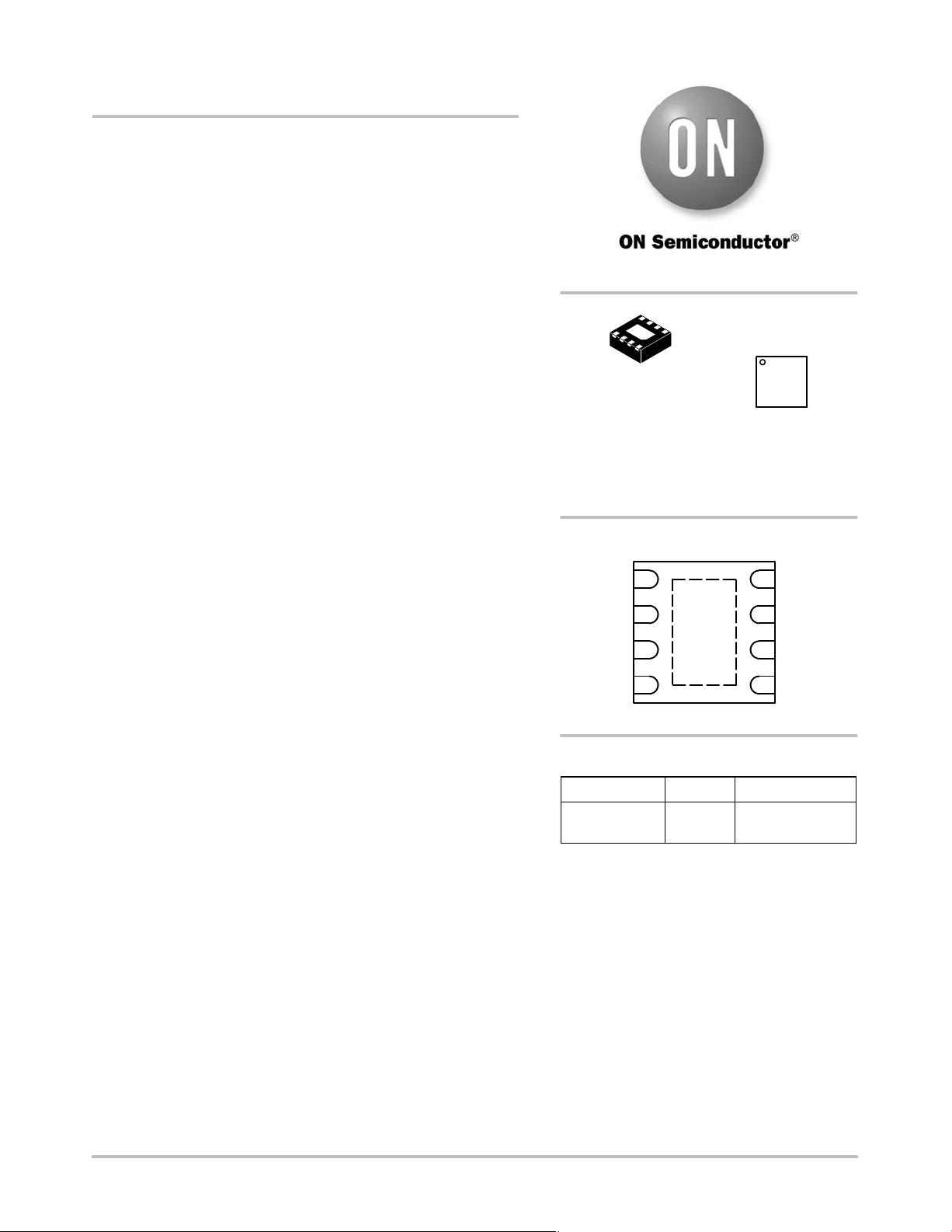
http://onsemi.com
MARKING
DIAGRAM
1
DFN8
CASE 506AA
AL = Specific Device Code
M = Date Code
G = Pb−Free Package
(Note: Microdot may be in either location)
PINOUT DIAGRAM
1
BST
EN
VCC
2
FLAG
3
4
PWM
1
ALMG
G
8
DRVH
SW
7
9
6
GND
DRVL
5
Typical Applications
• Power Management Solutions for Notebook systems
*For additional information on our Pb−Free strategy and soldering details, please
download the ON Semiconductor Soldering and Mounting Techniques
Reference Manual, SOLDERRM/D.
© Semiconductor Components Industries, LLC, 2011
February, 2011 − Rev. 1
1 Publication Order Number:
ORDERING INFORMATION
Device Package Shipping
NCP5911MNTBG DFN8
(Pb−Free)
†For information on tape and reel specifications,
including part orientation and tape sizes, please
refer to our Tape and Reel Packaging Specifications
Brochure, BRD8011/D.
3000 / Tape & Reel
†
NCP5911/D
Page 2
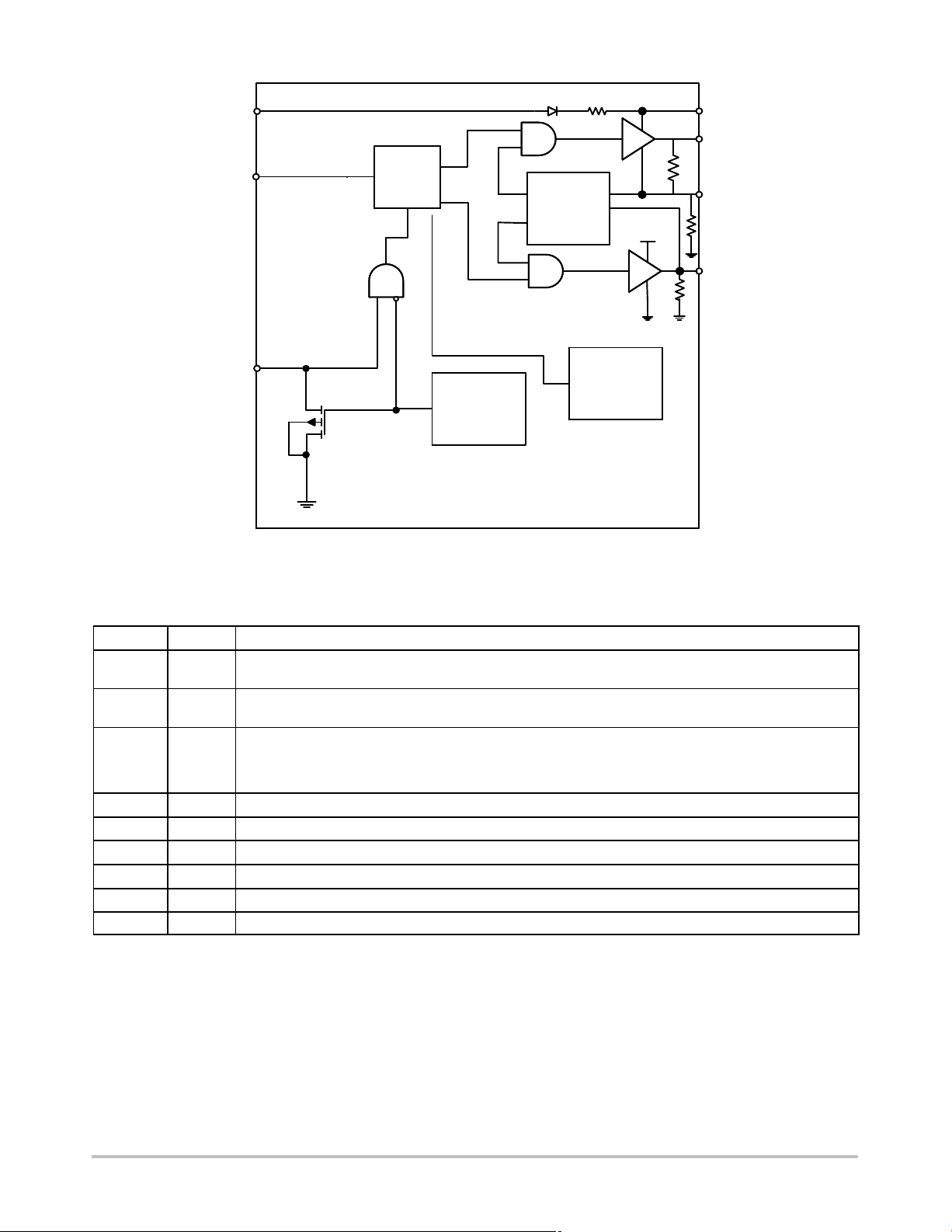
NCP5911
VCC
PWM
EN
Logic
UVLO
Fault
Figure 1. Block Diagram
Anti−Cross
Conduction
BST
DRVH
SW
VCC
DRVL
ZCD
Detection
PIN DESCRIPTIONS
Pin No. Symbol Description
1 BST Floating bootstrap supply pin for high side gate driver. Connect the bootstrap capacitor between this pin and
2 PWM Control input. The PWM signal has three distinctive states: Low = Low Side FET Enabled, Mid = Diode
3 EN Logic input. A logic high to enable the part and a logic low to disable the part. Three states logic input:
4 VCC
5 DRVL Low side gate drive output. Connect to the gate of low side MOSFET.
6 GND Bias and reference ground. All signals are referenced to this node.
7 SW Switch node. Connect this pin to the source of the high side MOSFET and drain of the low side MOSFET.
8 DRVH High side gate drive output. Connect to the gate of high side MOSFET.
9 FLAG Thermal flag. There is no electrical connection to the IC. Connect to ground plane.
the SW pin.
Emulation Enabled, High = High Side FET Enabled.
EN = High to enable the gate driver;
EN = Low to disable the driver;
EN = Mid to go into diode mode (both high and low side gate drive signals are low)
Power supply input. Connect a bypass capacitor (0.1 mF) from this pin to ground.
http://onsemi.com
2
Page 3
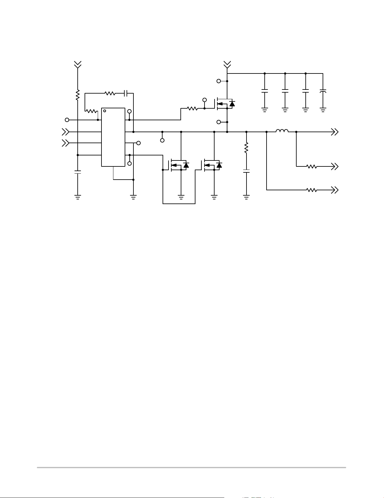
NCP5911
APPLICATION CIRCUIT
TP4
PWM
DRON
5V_POWER
R1
1.02
C5
1uF
R143
0.0
R164
0.0
NCP5911
BST
PWM
EN
VCC
PAD
HG
SW
GND
LG
C4
0.027uF
TP3
VREG_SW1_HG
VREG_SW1_OUT
VREG_SW1_LG
TP8
TP2
R142
0.0
TP6
TP7
Q9 Q10
NTMFS4851N NTMFS4851N
Figure 2. Application Circuit
TP1
TP5
VIN
Q1
NTMFS4821N
C1 C2 C3 CE9
4.7uF 4.7uF 4.7uF 390uF
L
235nH
R3
2.2
C6
2700pF
JP13_ETCH
JP14_ETCH
+
VCCP
CSN11
CSP11
http://onsemi.com
3
Page 4

NCP5911
ABSOLUTE MAXIMUM RATINGS
ELECTRICAL INFORMATION
Symbol Pin Name V
V
CC
Main Supply Voltage Input 6.5 V −0.3 V
MAX
BST Bootstrap Supply Voltage 35 V wrt/ GND
40 V v 50 ns wrt/ GND
6.5 V wrt/ SW
SW Switching Node (Bootstrap Supply Return) 35 V
40 V v 50 ns
DRVH High Side Driver Output BST + 0.3 V −0.3 V wrt/SW
−2 V (< 200 ns) wrt/SW
DRVL Low Side Driver Output VCC + 0.3 V −0.3 V DC
PWM DRVH and DRVL Control Input 6.5 V −0.3 V
EN Enable Pin 6.5 V −0.3 V
GND Ground 0 V 0 V
Stresses exceeding Maximum Ratings may damage the device. Maximum Ratings are stress ratings only. Functional operation above the
Recommended Operating Conditions is not implied. Extended exposure to stresses above the Recommended Operating Conditions may affect
device reliability.
*All signals referenced to AGND unless noted otherwise.
V
MIN
−0.3 V wrt/SW
−5 V
−10 V (200 ns)
−5 V (< 200 ns)
THERMAL INFORMATION
Symbol Parameter Value Unit
R
q
JA
T
J
T
A
T
STG
MSL Moisture Sensitivity Level − QFN Package 1
*The maximum package power dissipation must be observed.
2
Cu, 1 oz. thickness.
1. 1 in
2. JESD 51−7 (1S2P Direct−Attach Method) with 1 LFM.
Thermal Characteristic QFN Package (Note 1) 119 °C/W
Operating Junction Temperature Range (Note 2) 0 to 150 °C
Operating Ambient Temperature Range −40 to +100 °C
Maximum Storage Temperature Range −55 to +150 °C
http://onsemi.com
4
Page 5

NCP5911
NCP5911 ELECTRICAL CHARACTERISTICS (−40°C < T
< +100°C; 4.5 V < VCC < 5.5 V, 4.5 V < BST−SWN < 5.5 V,
A
4.5 V < BST < 30 V, 0 V < SWN < 21 V, unless otherwise noted)
Parameter
Test Conditions Min Typ Max Unit
SUPPLY VOLTAGE
VCC Operation Voltage
4.5 5.5 V
UNDERVOLTAGE LOCKOUT
VCC Start Threshold 3.8 4.35 4.5 V
VCC UVLO Hysteresis 150 200 250 mV
SUPPLY CURRENT
Shutdown Mode
ICC + I
Normal Mode ICC + I
Standby Current ICC + I
No loading on DRVH & DRVL
Standby Current ICC + I
No loading on DRVH & DRVL
, EN = GND 15 30
BST
, EN = 5 V, PWM = OSC 5.0 mA
BST
, EN = HIGH, PWM = LOW,
BST
, EN = HIGH, PWM = HIGH,
BST
0.9 mA
1.1 mA
mA
BOOTSTRAP DIODE
Forward Voltage
VCC = 5 V, forward bias current = 2 mA 0.1 0.4 0.6 V
PWM INPUT
PWM Input High
3.4 V
PWM Mid−State 1.3 2.7 V
PWM Input Low 0.7 V
ZCD Blanking Timer 350 ns
HIGH SIDE DRIVER
Output Impedance, Sourcing Current
Output Impedance, Sinking Current V
V
BST−VSW
BST−VSW
DRVH Rise Time trDRVH VCC = 5 V, 3 nF load, V
DRVH Fall Time tfDRVH
DRVH Turn−Off Propagation Delay tpdlDRVH
DRVH Turn−On Propagation Delay tpdhDRVH
V
CC
C
LOAD
C
LOAD
SW Pulldown Resistance SW to PGND 45
DRVH Pulldown Resistance DRVH to SW, BST−SW = 0 V 45
= 5 V 0.9 2.0
= 5 V 0.7 2.0
= 5 V 16 25 ns
=5 V
10 30 ns
15 45 ns
= 5 V, 3 nF load, V
= 3 nF
= 3 nF
BST−VSW
BST−VSW
11 18 ns
kW
kW
LOW SIDE DRIVER
Output Impedance, Sourcing Current
0.9 2.0
Output Impedance, Sinking Current 0.4 1.0
DRVL Rise Time trDRVL
DRVL Fall Time tfDRVL
DRVL Turn−Off Propagation Delay tpdlDRVL
DRVL Turn−On Propagation Delay tpdhDRVL
C
LOAD
C
LOAD
C
LOAD
C
LOAD
= 3 nF
= 3 nF
= 3 nF
= 3 nF
10 30 ns
5.0 25 ns
DRVL Pulldown Resistance DRVL to PGND, VCC = PGND 45
16 25 ns
11 15 ns
kW
W
W
W
W
http://onsemi.com
5
Page 6

NCP5911
NCP5911 ELECTRICAL CHARACTERISTICS (−40°C < T
4.5 V < BST < 30 V, 0 V < SWN < 21 V, unless otherwise noted)
Parameter UnitMaxTypMinTest Conditions
EN INPUT
Input Voltage High
Input Voltage Mid 1.35 1.8 V
Input Voltage Low 0.6 V
Input bias current −1.0 1.0
Fault mode Enable Pin Pulldown Current 4.0 30 mA
Propagation Delay Time 20 40 ns
SW NODE
SW Node Leakage Current
Zero Cross Detection Threshold Voltage −6.0 mV
< +100°C; 4.5 V < VCC < 5.5 V, 4.5 V < BST−SWN < 5.5 V,
A
3.3 V
20
mA
mA
http://onsemi.com
6
Page 7

NCP5911
Table 1. DECODER TRUTH TABLE
Input ZCD DRVL DRVH
PWM High (Enable High) ZCD Reset Low High
PWM Mid (Enable High) Positive Current Through the Inductor High Low
PWM Mid (Enable High) Zero Current Through the Inductor Low Low
PWM Low (Enable High) ZCD Reset High Low
Enable at Mid X Low Low
1V
1V
PWM
DRVH−SW
DRVL
Figure 3.
IL
Figure 4. Timing Diagram
http://onsemi.com
7
Page 8

NCP5911
APPLICATION INFORMATION
The NCP5911 gate driver is a single phase MOSFET
driver designed for driving N−channel MOSFETs in a
synchronous buck converter topology. The NCP5911 is
designed to work with ON Semiconductor’s NCP6131
multi−phase controller. This gate driver is optimized for
notebook applications.
Undervoltage Lockout
DRVH and DRVL are held low until VCC reaches 4.5 V
during startup. The PWM signal will control the gate status
when V
Three−State EN Signal
CC threshold is exceeded.
Undervoltage Lockout will de−assert the EN pin, which
will pull down the DRON pin of the controller as well.
When EN is set to the mid state, both DRVH and DRVL
are set low, to force diode mode operation.
PWM Input and Zero Cross Detect (ZCD)
The PWM input, along with EN and ZCD, control the state
of DRVH and DRVL.
When PWM is set high, DRVH will be set high after the
adaptive non−overlap delay. When PWM is set low, DRVL
will be set high after the adaptive non−overlap delay.
When PWM is set to the mid state, DRVH will be set low,
and after the adaptive non−overlap delay, DRVL will be set
high. DRVL remains high during the ZCD blanking time.
When the timer has expired, the SW pin will be monitored
for zero cross detection. After the detection, DRVL will be
set low.
Adaptive Non−overlap
Adaptive dead time control is used to avoid shoot−through
damage of the power MOSFETs. When the PWM signal
pulls high, DRVL will be set low and the driver will monitor
the gate voltage of the low side MOSFET. When the DRVL
voltage falls below the gate threshold, DRVH will be set to
high after the tpdh
DRVH delay. When PWM is set low, the
driver will monitor the gate voltage of the high side
MOSFET. When the DRVH−SWN voltage falls below the
top gate drive threshold, DRVL will be set to high after the
tpdh
DRVL delay.
Layout Guidelines
The layout for a DC−DC converter is very important. The
bootstrap and V
CC bypass capacitors should be placed close
to the driver IC.
Connect the GND pin to a local ground plane. The ground
plane can provide a good return path for gate drives and
reduce the ground noise. The thermal slug should be tied to
the ground plane for good heat dissipation. To minimize the
ground loop for the low side MOSFET, the driver GND pin
should be close to the low−side MOSFET source pin. The
gate drive trace should be routed to minimize its length. The
minimum width is 20 mils.
Gate Driver Power Loss Calculation
The gate driver power loss consists of the gate drive loss
and quiescent power loss.
The equation below can be used to calculate the power
dissipation of the gate driver. Q
for each main MOSFET and Q
GMF is the total gate charge
GSF is the total gate charge for
each synchronous MOSFET.
P
+
DRV
f
ƪ
2 n
SW
ǒnMF Q
) nSF Q
GMF
GSF
Ǔ
) I
CC
ƫ
V
(eq. 1)
CC
Also shown is the standby dissipation factor (ICC x VCC)
of the driver.
http://onsemi.com
8
Page 9

NCP5911
PACKAGE DIMENSIONS
DFN8 2x2
CASE 506AA−01
ISSUE E
2X
NOTE 4
PIN ONE
REFERENCE
2X
C0.15
C0.15
DETAIL B
C0.10
C0.08
SIDE VIEW
DETAIL A
1
8
K
e/2
e
BOTTOM VIEW
D
TOP VIEW
(A3)
D2
NOTES:
1. DIMENSIONING AND TOLERANCING PER
ASME Y14.5M, 1994 .
2. CONTROLLING DIMENSION: MILLIMETERS.
3. DIMENSION b APPLIES TO PLATED
TERMINAL AND IS MEASURED BETWEEN
0.15 AND 0.20 MM FROM TERMINAL TIP.
4. COPLANARITY APPLIES TO THE EXPOSED
PAD AS WELL AS THE TERMINALS.
MILLIMETERS
DIM MIN MAX
A 0.80 1.00
A1 0.00 0.05
A3 0.20 REF
b 0.20 0.30
D 2.00 BSC
D2 1.10 1.30
E 2.00 BSC
E2 0.70 0.90
e 0.50 BSC
0.30 REF
K
L 0.25 0.35
L1 −−− 0.10
A1
A
B
L
L
L1
E
A
SEATING
C
PLANE
DETAIL A
OPTIONAL
CONSTRUCTIONS
MOLD CMPDEXPOSED Cu
DETAIL B
OPTIONAL
CONSTRUCTION
RECOMMENDED
SOLDERING FOOTPRINT*
8X
4
L
PACKAGE
OUTLINE
1.30
E2
0.90
5
8X
b
8X
0.30
1
DIMENSIONS: MILLIMETERS
0.10 C
0.05 C
A
BB
NOTE 3
*For additional information on our Pb−Free strategy and soldering
details, please download the ON Semiconductor Soldering and
Mounting Techniques Reference Manual, SOLDERRM/D.
8X
0.50
0.50
PITCH
2.30
ON Semiconductor and are registered trademarks of Semiconductor Components Industries, LLC (SCILLC). SCILLC reserves the right to make changes without further notice
to any products herein. SCILLC makes no warranty, representation or guarantee regarding the suitability of its products for any particular purpose, nor does SCILLC assume any liability
arising out of the application or use of any product or circuit, and specifically disclaims any and all liability, including without limitation special, consequential or incidental damages.
“Typical” parameters which may be provided in SCILLC data sheets and/or specifications can and do vary in different applications and actual performance may vary over time. All
operating parameters, including “Typicals” must be validated for each customer application by customer’s technical experts. SCILLC does not convey any license under its patent rights
nor the rights of others. SCILLC products are not designed, intended, or authorized for use as components in systems intended for surgical implant into the body, or other applications
intended to support or sustain life, or for any other application in which the failure of the SCILLC product could create a situation where personal injury or death may occur. Should
Buyer purchase or use SCILLC products for any such unintended or unauthorized application, Buyer shall indemnify and hold SCILLC and its officers, employees, subsidiaries, affiliates,
and distributors harmless against all claims, costs, damages, and expenses, and reasonable attorney fees arising out of, directly or indirectly, any claim of personal injury or death
associated with such unintended or unauthorized use, even if such claim alleges that SCILLC was negligent regarding the design or manufacture of the part. SCILLC is an Equal
Opportunity/Affirmative Action Employer. This literature is subject to all applicable copyright laws and is not for resale in any manner.
PUBLICATION ORDERING INFORMATION
LITERATURE FULFILLMENT:
Literature Distribution Center for ON Semiconductor
P.O. Box 5163, Denver, Colorado 80217 USA
Phone: 303−675−2175 or 800−344−3860 Toll Free USA/Canada
Fax: 303−675−2176 or 800−344−3867 Toll Free USA/Canada
Email: orderlit@onsemi.com
N. American Technical Support: 800−282−9855 Toll Free
USA/Canada
Europe, Middle East and Africa Technical Support:
Phone: 421 33 790 2910
Japan Customer Focus Center
Phone: 81−3−5773−3850
http://onsemi.com
ON Semiconductor Website: www.onsemi.com
Order Literature: http://www.onsemi.com/orderlit
For additional information, please contact your local
Sales Representative
NCP5911/D
9
Page 10

 Loading...