

Page 1
NCP5424
Dual Synchronous
Buck Controller with Input
Current Sharing
The NCP5424 is a flexible dual N-channel synchronous buck
controller utilizing V2 control for fast transient response and
excellent line and load regulation. This highly versatile controller can
be configured as a single two phase output converter that draws
programmable amounts of current from two different input voltages or
all current from one supply. The NCP5424 can also be configured as
two independent out-of-phase controllers.
Using the NCP5424 in a current sharing input configuration is ideal
for applications where more power is required than is available from
one supply, such as video cards or other plug-in boards. When
configured as a dual output controller, the output of one controller can
be divided down and used as the reference for the second controller.
This tracking capability is useful in applications such as Double Data
Rate (DDR) Memory power where the termination voltage must track
VDD.
The NCP5424 provides a cycle-to-cycle current limit on
Controller 2 allowing the system to handle transient overcurrent
events and a hiccup mode overcurrent protection on Controller 1
allowing lossless short circuit protection. In addition, the NCP5424
provides Soft Start, undervoltage lockout, and built-in adaptive FET
nonoverlap time to prevent shoot through.
Features
• Hiccup Mode Current Limit (Controller 1)
• Cycle-to-Cycle Current Limit (Controller 2)
• Programmable Soft Start
• 100% Duty Cycle for Enhanced Transient Response
• 150 kHz to 600 kHz Programmable Frequency Operation
• Switching Frequency Set by Single Resistor
• Out-Of-Phase Synchronization Between the Channels Reduces the
Input Filter Requirement
• Undervoltage Lockout
Applications
• Video Graphics Card
• DDR Memory
• High Current (Two-Phase) Power Supplies
• Dual Output DC-DC Converters
http://onsemi.com
16
1
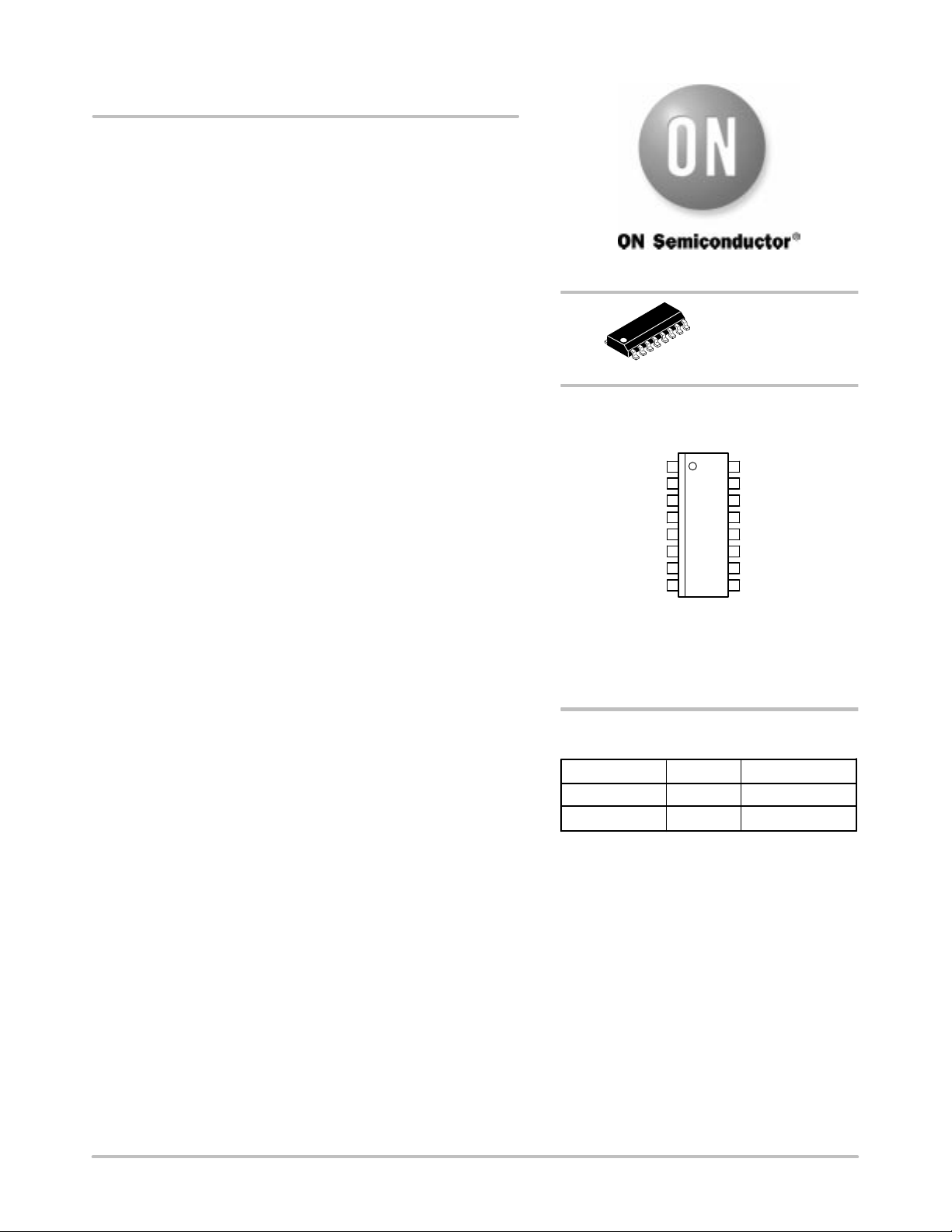
PIN CONNECTIONS AND
MARKING DIAGRAM
AWLYWW
SO-16
16
NCP5424
GATE(H)1
GATE(L)1
COMP1
ORDERING INFORMATION
Device Package Shipping
NCP5424D SO-16
NCP5424DR2
1
GND
BST
IS+1
IS-
V
FB1
A = Assembly Location
WL = Wafer Lot
Y = Year
WW = Work Week
SO-16
D SUFFIX
CASE 751B
GATE(H)2
GATE(L)2
V
CC
R
OSC
IS+2
V
FB+2
V
FB- 2
COMP2
48 Units/Rail
2500 Tape & Reel
Semiconductor Components Industries, LLC, 2003
June, 2003 - Rev. 3
1 Publication Order Number:
NCP5424/D
Page 2
5.0 V
12 V
C2
+
+
220 µFC1220 µF
NCP5424
C17
220 µF
++
C18
220 µF
3.3 V
0.1 µF
C3/4/5
+
680 µF/
4 V
R3
x k ± 1%
x k ± 1%
C6
R1
x k
R4
R2
x k
L2
1.3 µH/15 A
R5
5 k ± 1%
10 k ± 1%
R6
Q3
MTD60N03
Q4
MTD90N02
C8
.22 µF
U1
V
CC
GATE(H)1
GATE(L)1
IS+1
NCP5424
ISCOMP1
V
FB1
GATE(H)2
GATE(L)2
GND
C11
1.0 µF
BST
IS+2
V
FB+2
COMP2
V
FB- 2
R
OSC
R12
30.9 k
Q1Q2MTD60N03
MTD90N02
C14
0.1 µF
R17
4 k
C13
0.01 µF
L1
1.3 µH/15 A
C19/20/21
+
680 µF/
4 V
1.5 V @ 20 A
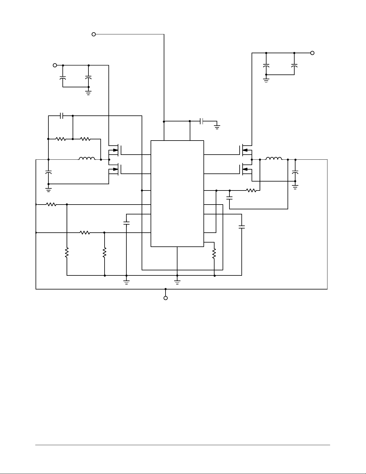
Figure 1. Two-Phase Buck Regulator Application, with Input Current Sharing
http://onsemi.com
2
Page 3
NCP5424
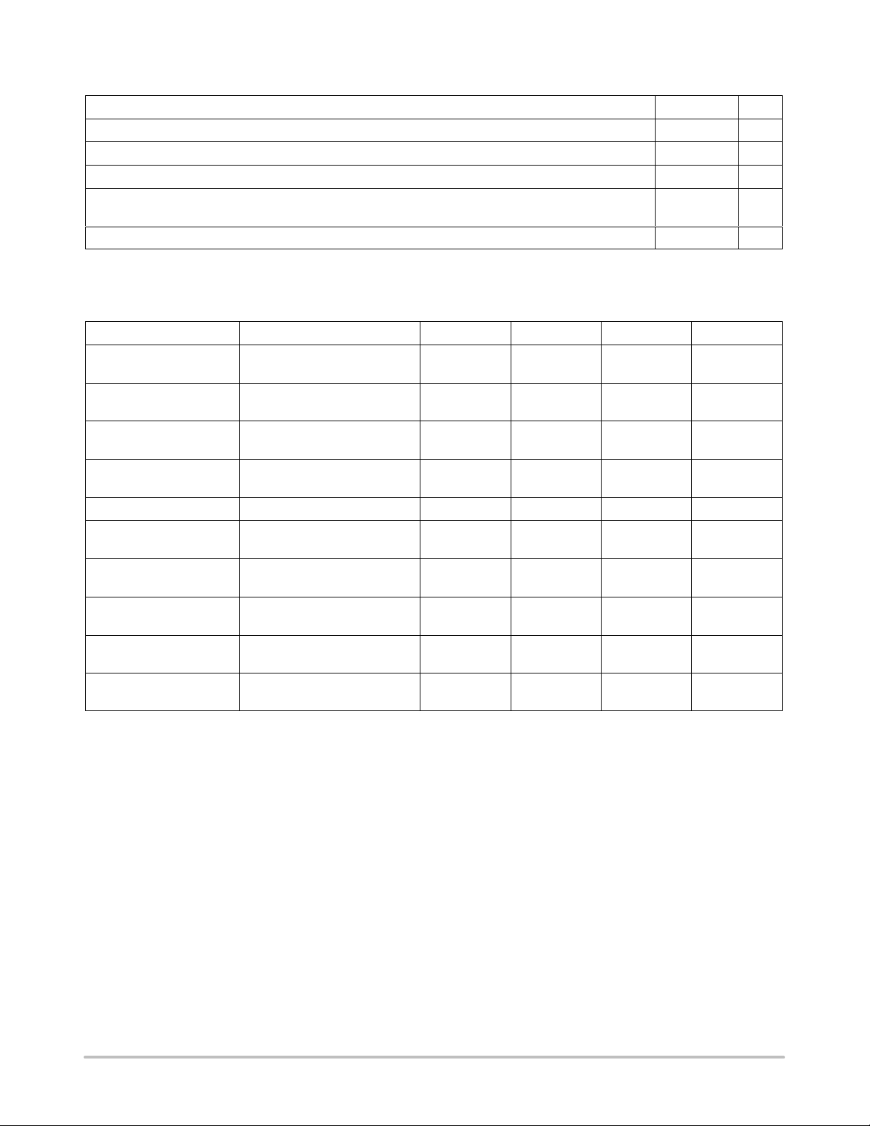
MAXIMUM RATINGS*
Rating Value Unit
Operating Junction Temperature, T
Storage Temperature Range, T
J
S
ESD Susceptibility (Human Body Model) 2.0 kV
Package Thermal Resistance, SO-16: Junction-to-Case, R
Junction-to-Ambient, R
θ
JC
θ
JA
Lead Temperature Soldering: Reflow: (SMD styles only) (Note 1) 230 peak °C
1. 60 second maximum above 183°C.
*The maximum package power dissipation must be observed.
MAXIMUM RATINGS
Pin Symbol Pin Name V
V
CC
IC Power Input 16 V -0.3 V N/A 1.5 A peak
MAX
V
MIN
I
SOURCE
150 °C
-65 to +150 °C
28
115
I
SINK
200 mA DC
°C/W
°C/W
COMP1, COMP2 Compensation Capacitor for
4.0 V -0.3 V 1.0 mA 3.5 mA
Channel 1 or 2
V
, V
FB1
FB+2
, V
FB- 2
Voltage Feedback Input for
5.0 V -0.3 V 1.0 mA 1.0 mA
Channel 1 or 2
BST Power Input for GATE(H)1, 2 20 V -0.3 V N/A 1.5 A peak
R
GATE(H)1
OSC
GATE(H)2 High-Side FET Driver
,
Oscillator Resistor 4.0 V -0.3 V 1.0 mA 1.0 mA
20 V -0.3 V 1.5 A peak
for Channel 1 or 2
GATE(L)1
GATE(L)2 Low-Side FET Driver for
,
16 V -0.3 V 1.5 A peak
Channel 1 or 2
GND Ground 0 V 0 V 1.5 A peak
IS+1, IS+2 Positive Current Sense for
6.0 V -0.3 V 1.0 mA 1.0 mA
Channel 1 or 2
IS- Negative Current Sense for
6.0 V -0.3 V 1.0 mA 1.0 mA
Channels 1 and 2
200 mA DC
200 mA DC
200 mA DC
200 mA DC
1.5 A peak
200 mA DC
1.5 A peak
200 mA DC
N/A
http://onsemi.com
3
Page 4
NCP5424
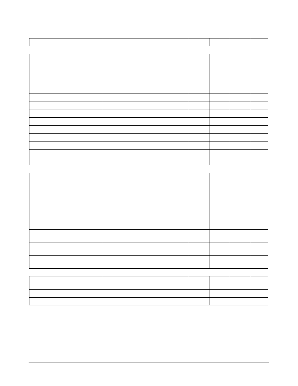
ELECTRICAL CHARACTERISTICS (0°C < T
10.8
V < V
< 13.2 V; 10.8 V < BST < 20 V, C
CC
Characteristic
< 70°C; 0°C < TJ < 125°C; R
A
GATE(H)1,2
= C
GATE(L)1,2
Test Conditions Min Typ Max Unit
= 1.0 nF, V
= 30.9 k, C
OSC
= 1.0 V; unless otherwise specified.)
FB+2
COMP1,2
= 0.1 µF,
Error Amplifier
VFB Bias Current V
V
Input Range Note 2 0 - 1.1 V
FB1(2)
COMP1,2 Source Current COMP1,2 = 1.2 V to 2.5 V; V
COMP1,2 Sink Current COMP1,2 = 1.2 V; V
Reference Voltage 1(2) COMP1 = V
COMP1,2 Max Voltage V
COMP1,2 Min Voltage V
= 0 V - 0.5 1.6 µA
FBX
= 0.8 V 15 30 60 µA
FB1(- 2)
= 1.2 V 15 30 60 µA
FB1(- 2)
; COMP2 = V
FB1
= 0.8 V 3.0 3.3 - V
FB1(- 2)
= 1.2 V - 0.25 0.35 V
FB1(- 2)
FB- 2
0.980 1.000 1.020 V
Open Loop Gain - - 95 - dB
Unity Gain Band Width - - 40 - kHz
PSRR @ 1.0 kHz - - 70 - dB
Transconductance - - 32 - mmho
Output Impedance - - 2.5 - MΩ
Input Offset, Error Amp. 2 - -3.0 0 3.0 mV
Error Amp. 2 Common Mode Range Note 2 1.75 2.0 - V
GATE(H) and GATE(L)
High Voltage (AC) Measure: VCC - GATE(L)1,2;
- 0 0.5 V
BST - GATE(H)1,2; Note 2
Low Voltage (AC) Measure:GA TE(L)1,2 or GATE(H)1,2; Note 2 - 0 0.5 V
Rise Time 1.0 V < GATE(L)1,2 < VCC - 1.0 V
- 20 50 ns
1.0 V < GATE(H)1,2 < BST - 1.0 V,
BST ≤ 14 V
Fall Time VCC - 1.0 > GATE(L)1,2 > 1.0 V
- 15 50 ns
BST - 1.0 > GATE(H)1,2 > 1.0 V,
BST ≤ 14 V
GATE(H) to GATE(L) Delay GATE(H)1,2 < 2.0 V, GATE(L)1,2 > 2.0 V
20 40 70 ns
BST ≤ 14 V
GATE(L) to GATE(H) Delay GATE(L)1,2 < 2.0 V, GATE(H)1,2 > 2.0 V;
20 40 70 ns
BST ≤ 14 V
GATE(H)1(2) and GATE(L)1(2)
pull-down.
Resistance to GND
Note 2
50 125 280 kΩ
PWM Comparator
PWM Comparator Offset V
= 0 V; Increase COMP1,2 until
FB1(- 2)
0.30 0.40 0.50 V
GATE(H)1,2 starts switching
Artificial Ramp Duty cycle = 50%, Note 2 60 105 150 mV
Minimum Pulse Width Note 2 - - 300 ns
2. Guaranteed by design, not 100% tested in production.
http://onsemi.com
4
Page 5
NCP5424
ELECTRICAL CHARACTERISTICS (continued) (0°C < T
10.8
V < V
< 13.2 V; 10.8 V < BST < 20 V, C
CC
GATE(H)1,2
= C
< 70°C; 0°C < TJ < 125°C; R
A
GATE(L)1,2
= 1.0 nF, V
= 30.9 k, C
OSC
= 1.0 V; unless otherwise specified.)
FB+2
COMP1,2
= 0.1 µF,
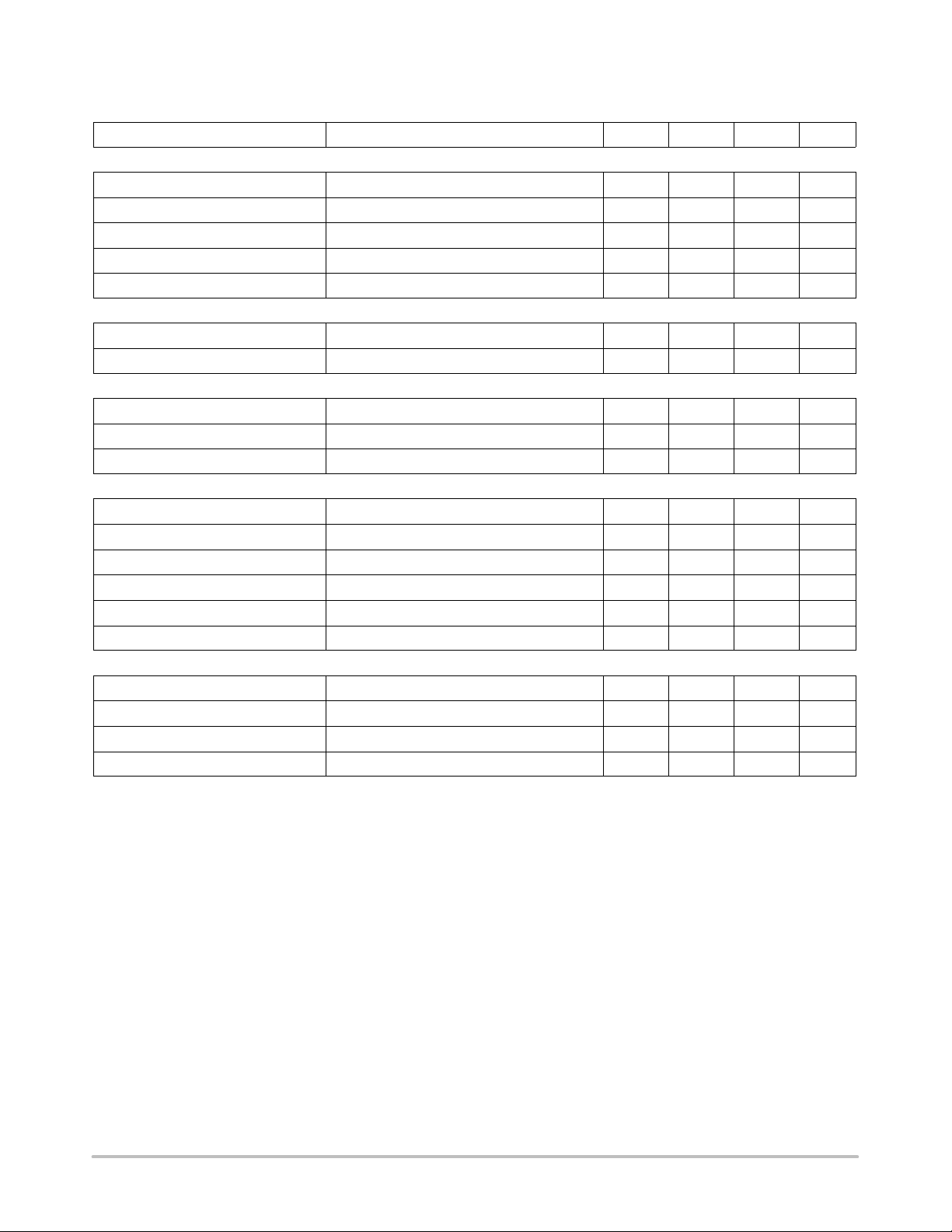
Characteristic UnitMaxTypMinTest Conditions
Oscillator
Switching Frequency R
Switching Frequency R
Switching Frequency R
R
Voltage R
OSC
= 61.9 k; Measure GATE(H)1; Note 3 112 150 188 kHz
OSC
= 30.9 k; Measure GATE(H)1 250 300 350 kHz
OSC
= 15.1 k; Measure GATE(H)1; Note 3 450 600 750 kHz
OSC
= 30.9 k, Note 3 0.970 1.000 1.030 V
OSC
Phase Difference - - 180 - °
Supply Currents
VCC Current COMP1,2 = 0 V (No Switching) - 13 17 mA
BST Current COMP1,2 = 0 V (No Switching) - 3.5 6.0 mA
Undervoltage Lockout
Start Threshold GATE(H) Switching; COMP1,2 charging 7.8 8.6 9.4 V
Stop Threshold GATE(H) not switching; COMP1,2 discharging 7.0 7.8 8.6 V
Hysteresis Start-Stop 0.5 0.8 1.5 V
Hiccup Mode Overcurrent Protection (Controller 1)
OVC Comparator Offset Voltage 0 V < IS+ 1 < 5.5 V, 0 V < IS- < 5.5 V 55 70 85 mV
Discharge Threshold - 0.20 0.25 0.30 V
IS+ 1 Bias Current 0 V < IS+ 1 < 5.5 V -1.0 0.1 1.0 µA
IS- Bias Current 0 V < IS- < 5.5 V -2.0 0.2 2.0 µA
OVC Common Mode Range - 0 - 5.5 V
OVC Latch COMP1 Discharge Current COMP1 = 1.0 V 2.0 5.0 8.0 µA
Cycle-to-Cycle Current Limit (Controller 2)
OVC Comparator Offset Voltage
0 V < IS+ 2 < 5.5 V, 0 V < IS- < 5.5 V 55 70 85 mV
IS+ 2 Bias Current 0 V < IS+ 2 < 5.5 V -1.0 0.1 1.0 µA
OVC Common Mode Range - 0 - 5.5 V
OVC Latch COMP2 Discharge Current COMP = 1.0 V 0.3 1.2 3.5 mA
3. Guaranteed by design, not 100% tested in production.
http://onsemi.com
5
Page 6

NCP5424
PACKAGE PIN DESCRIPTION
PIN # SYMBOL FUNCTION
1 GATE(H)1 High Side Switch FET driver pin for channel 1.
2 GATE(L)1 Low Side Synchronous FET driver pin for channel 1.
3 GND Ground pin for all circuitry contained in the IC. This pin is internally bonded to the substrate of the IC.
4 BST Power input for GATE(H)1 and GATE(H)2 pins.
5 IS+1 Positive input for channel 1 overcurrent comparator.
6 IS- Negative input for channels 1 and 2 overcurrent comparator.
7 V
FB1
8 COMP1 Channel 1 Error Amp output. PWM Comparator reference input. A capacitor to LGND provides Error
Error amplifier inverting input for channel 1.
Amp compensation. The same capacitor provides Soft Start timing for channel 1. This pin also disables the channel 1 output when pulled below 0.3 V.
9 COMP2 Channel 2 Error Amp output. PWM Comparator reference input. A capacitor to LGND provides Error
Amp compensation and Soft Start timing for channel 2. Channel 2 output is disabled when this pin is
pulled below 0.3 V.
10 V
11 V
FB- 2
FB+2
Error amplifier inverting input for channel 2.
Error amplifier noninverting input for channel 2.
12 IS+2 Positive input for channel 2 overcurrent comparator.
13 R
14 V
OSC
CC
Oscillator frequency pin. A resistor from this pin to ground sets the oscillator frequency.
Input Power supply pin.
15 GATE(L)2 Low Side Synchronous FET driver pin for channel 2.
16 GATE(H)2 High Side Switch FET driver pin for channel 2.
http://onsemi.com
6
Page 7
NCP5424
2
IS+1
IS-
IS+2
8.6 V
7.8 V
−
70 mV
−
70 mV
CC
R
OSC
CURRENT
SOURCE
OSC
PWM
Comparator 1
0.40 V
PWM
Comparator 2
GEN
CLK1
CLK2
−
+
RAMP1
−
+
RAMP2
RAMP1
S
Reset
Dominant
R
S
Reset
Dominant
R
RAMP2
BST
V
CC
BST
V
CC
BST
GATE(H)1
GATE(L)1
GATE(H)
GATE(L)2
V
BIAS
+
−
+
V
CC
−
+
+
−
+
+
−
FAULT
Q
S
Set
Dominant
R
E/A OFF
−
+
0.25 V
−
+
5 A
1.0 V
V
FB+2
E/A OFF
−
+
E/A2
COMP2
1.2 mA
FAULT
GND
+
V
0.40 V
FB- 2
+
−
−
E/A1
V
FB1
COMP1
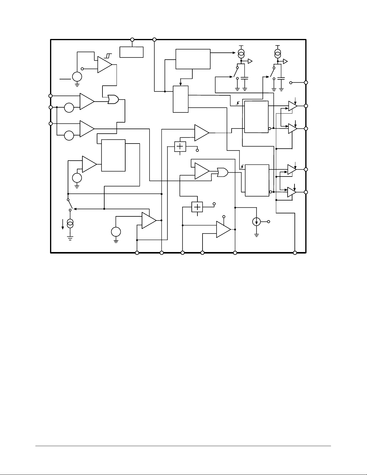
Figure 2. Block Diagram
http://onsemi.com
7
Page 8
NCP5424
APPLICATIONS INFORMATION
THEORY OF OPERATION
The NCP5424 is a dual output or single two-phase power
supply controller that utilizes the V2 control method. Two
synchronous V2 buck regulators can be built using a single
controller or a single output converter that draws
programmable amounts of current from two input voltages.
The fixed-frequency architecture, driven from a common
oscillator, ensures a 180° phase differential between
channels.
V2 Control Method
The V2 method of control uses a ramp signal that is
generated by the ESR of the output capacitors. This ramp is
proportional to the AC current through the main inductor
and is offset by the DC output voltage. This control scheme
inherently compensates for variation in either line or load
conditions, since the ramp signal is generated from the
output voltage itself. The V
2
method differs from traditional
techniques such as voltage mode control, which generates an
artificial ramp, and current mode control, which generates
a ramp using the inductor current.
-
PWM
+
RAMP
Slope
Compensation
COMP
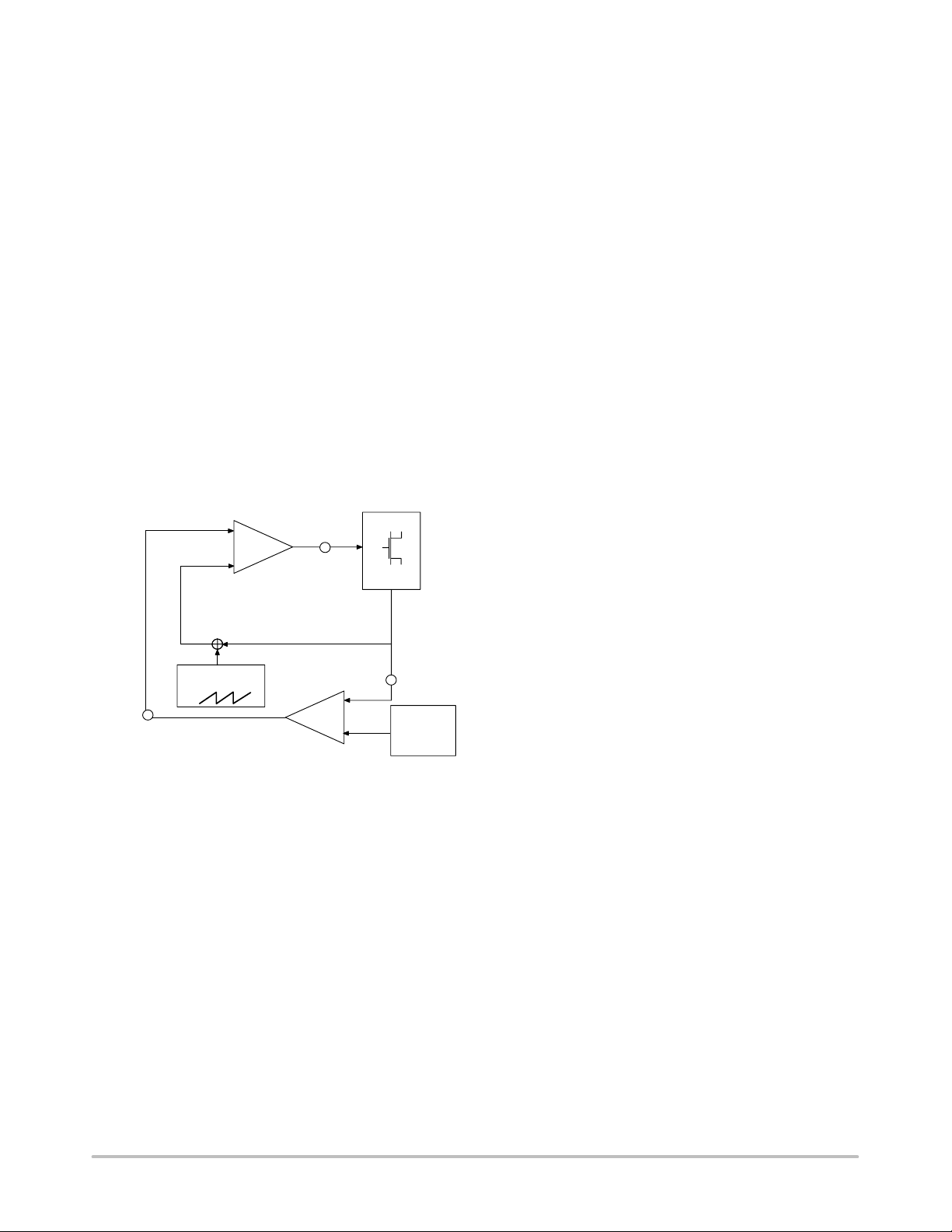
Figure 3. V2 Control with Slope Compensation
Error
Signal
GATE(H)
GATE(L)
Error
Amplifier
Output
Voltage
V
FB
-
+
Reference
Voltage
The V2 control method is illustrated in Figure 3. The
output voltage generates both the error signal and the ramp
signal. Since the ramp signal is simply the output voltage, it
is affected by any change in the output, regardless of the
origin of that change. The ramp signal also contains the DC
portion of the output voltage, allowing the control circuit to
drive the main switch to 0% or 100% duty cycle as required.
A variation in line voltage changes the current ramp in the
inductor, which causes the V
2
control scheme to compensate
the duty cycle. S ince a ny v ariation i n i nductor c urrent m odifies
the ramp signal, as in current mode control, the V2 control
scheme offers the same advantages in line transient response.
A variation in load current will affect the output voltage,
modifying the ramp signal. A load step immediately changes
the state of the comparator output, which controls the main
switch. The comparator response time and the transition
speed of the main switch determine the load transient
response. Unlike traditional control methods, the reaction
time to the output load step is not related to the crossover
frequency of the error signal loop.
The error signal loop can have a low crossover frequency,
since the transient response is handled by the ramp signal
loop. The main purpose of this ‘slow’ feedback loop is to
provide DC accuracy. Noise immunity is significantly
improved, since the error amplifier bandwidth can be rolled
off at a low frequency. Enhanced noise immunity improves
remote sensing of the output voltage, since the noise
associated with long feedback traces can be effectively
filtered.
Line and load regulation is drastically improved because
there are two independent control loops. A voltage mode
controller relies on the change in the error signal to
compensate for a deviation in either line or load voltage.
This change in the error signal causes the output voltage to
change corresponding to the gain of the error amplifier,
which is normally specified as line and load regulation. A
current mode controller maintains a fixed error signal during
line transients, since the slope of the ramp signal changes in
this case. However , r egulation o f l oad t ransients still requires
a change in the error signal. The V
2
method of control
maintains a f ixed e rror s ignal f or b oth l ine a nd l oad v ariation,
since the ramp signal is affected by both line and load.
The stringent load transient requirements of modern
microprocessors require the output capacitors to have very
low ESR. T he r esulting s hallow s lope i n t he o utput r ipple can
lead to p ulse w idth j itter a nd variation caused by b oth r andom
and synchronous noise. A ramp waveform generated in the
oscillator is added to the r amp s ignal f rom the o utput v oltage
to provide the proper voltage ramp at the beginning of each
switching cycle. This s lope c ompensation i ncreases t he n oise
immunity particularly at higher duty cycle (above 50%).
Start Up
The NCP5424 features a programmable Soft Start
function, which is implemented through the Error Amplifier
and the external Compensation Capacitor. This feature
prevents stress to the power components and overshoot of
the output voltage during start-up. As power is applied to the
regulator, the NCP5424 Undervoltage Lockout circuit
(UVL) monitors the IC’s supply voltage (V
). The UVL
CC
circuit resets an internal fault latch when the input voltage
exceeds 8.6 volts. This fault latch disables the error
amplifiers until it is reset. Once the amplifiers are enabled,
they start charging the compensation capacitors with a 30 uA
constant current that causes a linear voltage ramp. The
output of the error amplifier is connected internally to the
negative input of the PWM comparator. The comparator’s
positive input is connected back to the feedback voltage pin
through a 0.45-volt offset. With the feedback voltage
starting at zero, the offset voltage forces the comparator
high, which prevents resetting the RS latches that control the
output drivers. Once the compensation capacitor voltage
reaches 0.45 volts, the PWM comparator will switch and
http://onsemi.com
8
Page 9
NCP5424
allow a short PWM pulse. This pulse will gradually increase
in width as the voltage ramp on the Compensation Capacitor
continues to rise. This process will continue until the output
voltage reaches the designed value set by the feed back
resistors and the parts 1.0-volt reference voltage. Thus the
user can determine both soft start and power sequence
functions by selecting the compensation capacitors and
simply knowing that the amplifiers charge these capacitors
with 30 uA and that the threshold for starting PWM pulses
is 0.45 volts.
V
8.6 V
0.45 V
UVLO STAR TUP NORMAL OPERATION
t
S
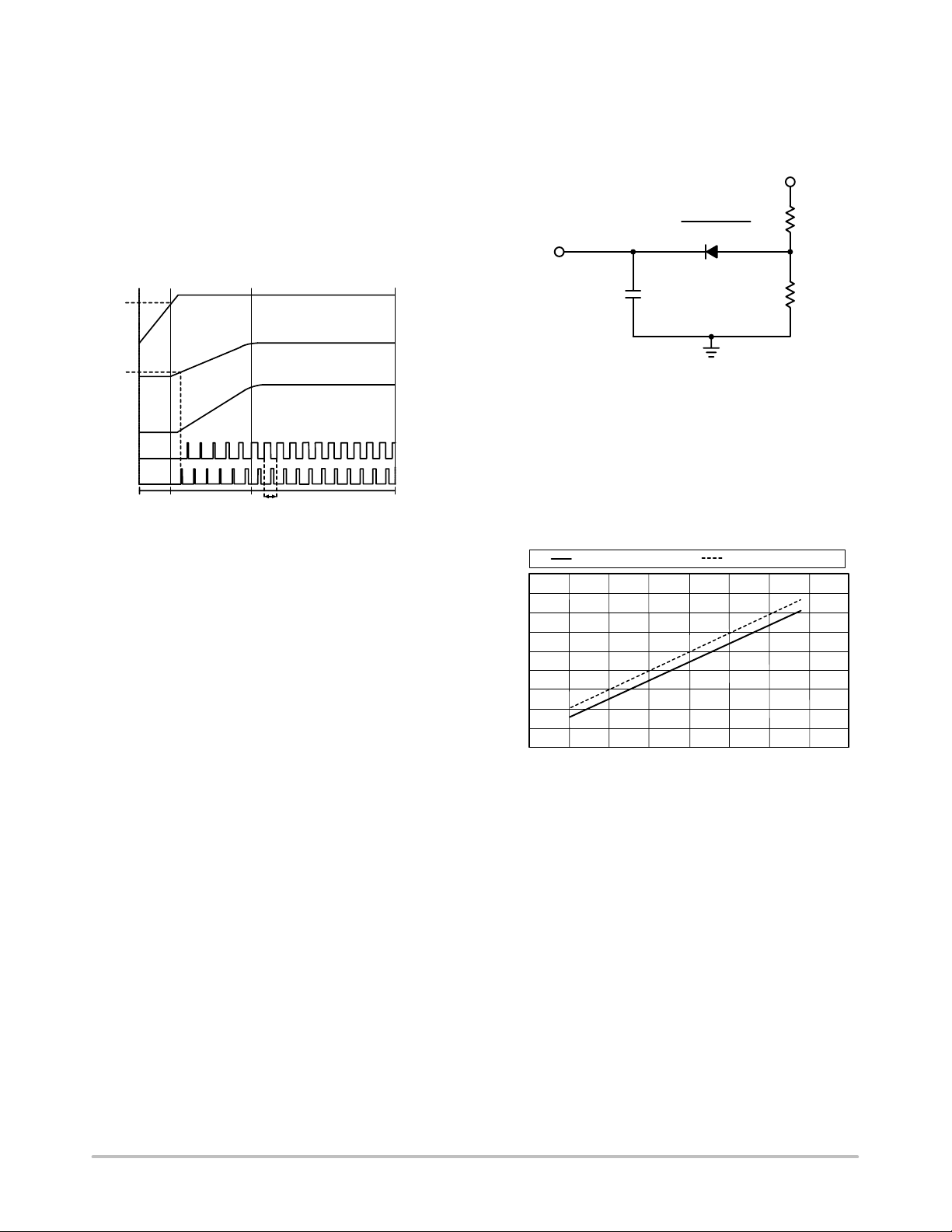
Figure 4. Idealized Waveforms
IN
V
COMP
V
FB
GATE(H)1
GATE(H)2
buildup of negative currents that arise during a long start
interval where the bottom FET of controller 2 is on. For
applications where there are two outputs, this problem can
not occur.
V
IN
(VIN - 1.15)
0.958
COMP2
Comp
Cap
k
1.2 k
Figure 5. Preventing Reverse Current
Gate Charge Effect on Switching Times
When using the onboard gate drivers, the gate charge has
an important effect on the switching times of the FETs. A
finite amount of time is required to charge the effective
capacitor seen at the gate of the FET. Therefore, the rise and
fall times rise linearly with increased capacitive loading,
according to the following graphs.
Normal Operation
During normal operation, the duty cycle of the gate drivers
remains approximately constant as the V2 control loop
maintains the regulated output voltage under steady state
conditions. Variations in supply line or output load
conditions will result in changes in duty cycle to maintain
regulation.
Zero Current Start Up in Single Output Shared Input
Current Applications
One problem that occurs with dual controllers when
connected as a single output is that reverse currents can
occur during zero load conditions. As the two controllers
start up and start delivering current, if there is no load a
reverse current will develop in the inductor of controller 2
that is equal and opposite the current in the controller 1
inductor. When the controller 2 starts to deliver power this
reverse current will flow backwards through the top FET
back into the supply. In the extreme this can cause the supply
to over voltage and/or shut down. Fortunately, there are
several ways to deal with this problem. One is to simply
insure the part has a minimum load. Another is illustrated in
Figure 5, where a diode and voltage divider biases the
controller 2 Compensation Capacitor above the 0.45 V soft
start threshold, such that the controller starts switching
without a soft start delay. The effect of this is to eliminate the
Average Fall Time Average Rise Time
90
80
70
60
50
40
30
Fall/Rise Time (ns)
20
10
0
01234567
Load (nF)
8
Figure 6. Average Rise and Fall Times
Transient Response
The 150 ns reaction time of the control loop provides fast
transient response to any variations in input voltage and
output current. Pulse-by-pulse adjustment of duty cycle is
provided to quickly ramp the inductor current to the required
level. Since the inductor current cannot be changed
instantaneously, regulation is maintained by the output
capacitors during the time required to slew the inductor
current. For better transient response, several high
frequency and bulk output capacitors are usually used.
http://onsemi.com
9
Page 10

NCP5424
Out-of-Phase Synchronization
In out-of-phase synchronization, the turn-on of the
second channel is delayed by half the switching cycle. This
delay is supervised by the oscillator, which supplies a clock
signal to the second channel which is 180° out of phase with
the clock signal of the first channel.
The advantages of out-of-phase synchronization are
many. Since the input current pulses are interleaved with one
another, the overlap time is reduced. The effect of this
overlap reduction is to reduce the input filter requirement,
allowing the use of smaller components. In addition, since
peak current occurs during a shorter time period, emitted
EMI is also reduced, thereby reducing shielding
requirements.
Overvoltage Protection
Overvoltage Protection (OVP) is provided as a result of
the normal operation of the V2 control method and requires
no additional external components. The control loop
responds to an overvoltage condition within 150 ns, turning
off the upper MOSFET and disconnecting the regulator
from its input voltage. This results in a crowbar action to
clamp the output voltage preventing damage to the load. The
regulator remains in this state until the overvoltage
condition ceases.
Input Current Sharing
In contemporary high-end applications, part of a system
may require more power than is available from one supply.
The NCP5424 dual controller can address this requirement
in two ways.
In many cases, it is sufficient to be able to set the input
power sharing as a ratio so that one source always supplies
a certain percentage of the total. This is achieved by having
the Error Amplifier inputs from Slave side, Controller Two,
brought to external pins so its’ reference is available.
Current information from the Master, Controller One,
provides a reference for the Slave. Current information from
the Slave is fed back to the error amplifier’s inverting input.
The Slave will try to adjust its current to match the current
information fed to its reference input from the Master. If this
information is 1/2 the voltage developed across the Master’s
output inductor, the Slave will run at half current and supply
a percentage, nominally 33% in this case, of the total current.
In other applications however, the user may not only wish
to draw a percentage of power from one source, but also may
need to limit the power drawn from that source. The Slave
has a Cycle-By-Cycle current limit. In this case, the Slave
can be programmed to budget the maximum input power.
For example, a designer may wish to draw equal amounts of
power from two 5-volt sources, but only 2 amps are
available from one of the supplies. In this case, the dual
controller will draw equally from the two sources up to a
total of 4 amps. At this point, the Slave controller goes into
current limit and draws no more than its preset budget. The
Master continues to supply the remaining output current up
to the maximum that the application requires.
Current Limiting
The NCP5424 employs two types of current limits.
Controller One has a Hiccup Mode Current Limit and
Controller Two has Cycle-By-Cycle current limit. Any
overcurrent condition on Controller One results in the
immediate shutdown of both output phases. In a dual output
application, independent current limits are not supported.
The NCP5424 has two current limiting amplifiers that
have a built in 70 mV offset. These differential amplifiers
have a common mode range from zero to 5.5 volts and low
input current. They share a common negative input that in
single output voltage application is not a limitation.
However in dual output applications independent current
limits are not supported.
Once a voltage greater than 70 mV is applied to the current
limiting amplifier of Controller 2; it produces an output that,
as shown in the block diagram, resets the output RS flip flop.
This ends the PWM pulse for the particular cycle and in so
doing, limits the energy delivered to the load on a
cycle-by-cycle basis. One advantage of this current limiting
scheme is that the NCP5424 will limit transient currents and
will resume normal operation the cycle after the transient
goes away.
A second benefit is that this action of limiting the PWM
pulse width means that in an input power sharing
application, one controller can be current limiting while the
other supplies the remaining current needs.
The fault latch immediately turns off the error amplifier
and discharges both COMP capacitors. The capacitor
connected to COMP1 is discharged through a 5.0 A current
sink in order to provide timing for the reset cycle. When
COMP1 has fallen below 0.25 V, a comparator resets the
fault latch and error amplifier 1 begins to charge COMP1
with a 30 A source current. When COMP1 exceeds the
feedback voltage plus the PWM Comparator offset voltage,
the normal switching cycle will resume. If the short circuit
condition persists through the restart cycle, the overcurrent
reset cycle will repeat itself until the short circuit is removed,
resulting in small “hiccup” output pulses while the COMP
capacitor charges and discharges. Please see the section
titled “Current Sharing Compensation Capacitor Selection”
for proper Comp capacitor selection.
Cycle-By-Cycle current limit controls the amount of
current available from Controller 2. Controller 2 has a
current limiting comparator that, by truncating the
respective controller’s PWM pulse width, limits the
available current on a pulse-by-pulse basis. This
comparator has a built in 70 mV offset that provides a
reference for setting current limit.
Output Enable
On/Off control of the regulator outputs can be
implemented by pulling the COMP pins low. The COMP
pins must be driven below the 0.40 V PWM comparator
offset voltage in order to disable the switching of the GATE
drivers.
http://onsemi.com
10
Page 11
NCP5424
DESIGN GUIDELINES
Definition of the design specifications
The output voltage tolerance can be affected by any or all
of the following:
1. buck regulator output voltage setpoint accuracy;
2. output voltage change due to discharging or charging
of the bulk decoupling capacitors during a load
current transient;
3. output voltage change due to the ESR and ESL of the
bulk and high frequency decoupling capacitors,
circuit traces, and vias;
4. output voltage ripple and noise.
Budgeting the tolerance is left to the designer who must
consider all of the above effects and provide an output
voltage that will meet the specified tolerance at the load.
The designer must also ensure that the regulator
component temperatures are kept within the manufacturer’s
specified ratings at full load and maximum ambient
temperature.
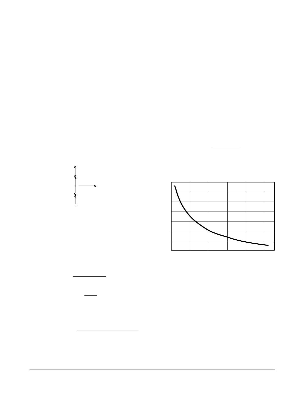
Selecting Feedback Divider Resistors
V
OUT
R1
V
FB
R2
VL = output inductor voltage drop due to inductor wire
DC resistance;
VIN = buck regulator input voltage;
V
= low side FET voltage drop due to R
LFET
Selecting the Switching Frequency
DS(ON)
.
Selecting the switching frequency is a trade-off between
component size and power losses. Operation at higher
switching frequencies allows the use of smaller inductor and
capacitor values. Nevertheless, it is common to select lower
frequency operation because a higher frequency results in
lower efficiency due to MOSFET gate charge losses.
Additionally, the use of smaller inductors at higher
frequencies results in higher ripple current, higher output
voltage ripple, and lower efficiency at light load currents.
The value of the oscillator resistor is designed to be
linearly related to the switching period. If the designer
prefers not to use Figure 8 to select the necessary resistor, the
following equation quite accurately predicts the proper
resistance for room temperature conditions.
R
OSC
21700 f
2.31f
SW
SW
where:
R
= oscillator resistor in kΩ;
OSC
fSW = switching frequency in kHz.
800
700
600
Figure 7. Selecting Feedback Divider Resistors
The feedback pins (V
) are connected to external
FB1(2)
resistor dividers to set the output voltages. The error
amplifier is referenced to 1.0 V and the output voltage is
determined by selecting resistor divider values. Resistor R1
is selected based on a design trade-off between efficiency
and output voltage accuracy. The output voltage error can be
estimated due to the bias current of the error amplifier
neglecting resistor tolerance:
Error%
1 106 R1
1
100%
R2 can be sized after R1 has been determined:
R2 R1
Calculating Duty Cycle
1
1
V
OUT
The duty cycle of a buck converter (including parasitic
losses) is given by the formula:
Duty Cycle D
OUT
VIN V
(V
LFET
HFET
V
VL)
HFET
V
L
V
where:
V
= buck regulator output voltage;
OUT
V
= high side FET voltage drop due to R
HFET
DS(ON)
500
400
300
Frequency (kHz)
200
100
10 20 30 40 50 60
R
Figure 8. Switching Frequency
Selection of the Output Inductor
OSC (k)
The inductor should be selected based on its inductance,
current capability, and DC resistance. Increasing the
inductor value will decrease output voltage ripple, but
degrade transient response. There are many factors to
consider in selecting the inductor including cost, efficiency,
EMI and ease of manufacture. The inductor must be able to
handle the peak current at the switching frequency without
saturating, and the copper resistance in the winding should
be kept as low as possible to minimize resistive power loss.
There are a variety of materials and types of magnetic
cores that could be used for this application. Among them
are ferrites, molypermalloy cores (MPP), amorphous and
;
powdered iron cores. Powdered iron cores are very
http://onsemi.com
11
Page 12

NCP5424
commonly used. Powdered iron cores are very suitable due
to its high saturation flux density and have low loss at high
frequencies, a distributed gap and exhibit very low EMI.
The minimum value of inductance which prevents
inductor saturation or exceeding the rated FET current can
be calculated as follows:
L
MIN
fSW V
(V
IN(MIN)
V
IN(MIN)
OUT)VOUT
I
SW(MAX)
where:
L
= minimum inductance value;
MIN
V
V
= minimum design input voltage;
IN(MIN)
= output voltage;
OUT
fSW = switching frequency;
I
SW(MAX)
- maximum design switch current.
The inductor ripple current can then be determined:
V
(1 D)
I
OUT
L
L f
SW
where:
∆I
= inductor ripple current;
L
V
= output voltage;
OUT
L = inductor value;
D = duty cycle.
fSW = switching frequency
The designer can now verify if the number of output
capacitors will provide an acceptable output voltage ripple
(1.0% of output voltage is common). The formula below is
used:
V
ESR
OUT
MAX
I
L
Rearranging we have:
V
ESR
MAX
OUT
I
L
where:
ESR
∆V
= maximum allowable ESR;
MAX
= 1.0% × V
OUT
= maximum allowable output
OUT
voltage ripple ( budgeted by the designer );
∆IL = inductor ripple current;
V
= output voltage.
OUT
The number of output capacitors is determined by:
ESR
Number of capacitors
ESR
CAP
MAX
where:
ESR
= maximum ESR per capacitor (specified in
CAP
manufacturer’s data sheet).
The designer must also verify that the inductor value
yields reasonable inductor peak and valley currents (the
inductor current is a triangular waveform):
I
I
L(PEAK)
I
OUT
L
2
where:
I
L(PEAK)
I
OUT
= inductor peak current;
= load current;
∆IL = inductor ripple current.
I
I
L(VALLEY)
I
OUT
L
2
where:
I
L(VALLEY)
Selection of the Output Capacitors
= inductor valley current.
These components must be selected and placed carefully
to yield optimal results. Capacitors should be chosen to
provide acceptable ripple on the regulator output voltage.
Key specifications for output capacitors are their ESR
(Equivalent Series Resistance), and ESL (Equivalent Series
Inductance). For best transient response, a combination of
low value/high frequency and bulk capacitors placed close
to the load will be required.
In order to determine the number of output capacitors the
maximum voltage transient allowed during load transitions
has to be specified. The output capacitors must hold the
output voltage within these limits since the inductor current
can not change with the required slew rate. The output
capacitors must therefore have a very low ESL and ESR.
The voltage change during the load current transient is:
V
OUT
I
OUT
ESL
ESR
t
C
t
TR
OUT
where:
∆I
/ ∆t = load current slew rate;
OUT
∆I
= load transient;
OUT
∆t = load transient duration time;
ESL = Maximum allowable ESL including capacitors,
circuit traces, and vias;
ESR = Maximum allowable ESR including capacitors
and circuit traces;
t
= output voltage transient response time.
TR
The designer has to independently assign values for the
change in output voltage due to ESR, ESL, and output
capacitor discharging or charging. Empirical data indicates
that most of the output voltage change (droop or spike
depending on the load current transition) results from the
total output capacitor ESR.
The maximum allowable ESR can then be determined
according to the formula:
V
ESR
MAX
I
ESR
OUT
where:
∆V
= change in output voltage due to ESR (assigned
ESR
by the designer)
Once the maximum allowable ESR is determined, the
number of output capacitors can be found by using the
formula:
ESR
Number of capacitors
ESR
CAP
MAX
where:
ESR
= maximum ESR per capacitor (specified in
CAP
manufacturer’s data sheet).
ESR
= maximum allowable ESR.
MAX
http://onsemi.com
12
Page 13

NCP5424
The actual output voltage deviation due to ESR can then
be verified and compared to the value assigned by the
designer:
V
ESR
I
OUT
ESR
MAX
Similarly, the maximum allowable ESL is calculated from
the following formula:
ESL
MAX
Selection of the Input Inductor
V
ESL
I
t
A common requirement is that the buck controller must
not disturb the input voltage. One method of achieving this
is by using an input inductor and a bypass capacitor. The
input inductor isolates the supply from the noise generated
in the switching portion of the buck regulator and also limits
the inrush current into the input capacitors upon power up.
The inductor’s limiting effect on the input current slew rate
becomes increasingly beneficial during load transients. The
worst case is when the load changes from no load to full load
(load step), a condition under which the highest voltage
change across the input capacitors is also seen by the input
inductor. The inductor successfully blocks the ripple current
while placing the transient current requirements on the input
bypass capacitor bank, which has to initially support the
sudden load change.
The minimum inductance value for the input inductor is
therefore:
V
(dIdt)
MAX
L
IN
where:
LIN = input inductor value;
∆V = voltage seen by the input inductor during a full load
swing;
(dI/dt)
= maximum allowable input current slew rate.
MAX
The designer must select the LC filter pole frequency so
that at least 40 dB attenuation is obtained at the regulator
switching frequency . The LC filter is a double-pole network
with a slope of -2.0, a roll-off rate of -40 dB/dec, and a
corner frequency:
2 LC
1
f
C
where:
L = input inductor;
C = input capacitor(s).
SELECTION OF THE POWER FET
FET Basics
The use of a MOSFET as a power switch is compelled by
two reasons: 1) high input impedance; and 2) fast switching
times. The electrical characteristics of a MOSFET are
considered to be nearly those of a perfect switch. Control
and drive circuitry power is therefore reduced. Because the
input impedance is so high, it is voltage driven. The input of
the MOSFET acts as if it were a small capacitor, which the
driving circuit must charge at turn on. The lower the drive
impedance, the higher the rate of rise of V
, and the faster
GS
the turn-on time. Power dissipation in the switching
MOSFET consists of 1) conduction losses, 2) leakage
losses, 3) turn-on switching losses, 4) turn-off switching
losses, and 5) gate-transitions losses. The latter three losses
are proportional to frequency.
The most important aspect of FET performance is the
Static Drain-To-Source On-Resistance (R
DS(ON)
), which
affects regulator efficiency and FET thermal management
requirements. The On-Resistance determines the amount of
current a FET can handle without excessive power
dissipation that may cause overheating and potentially
catastrophic failure. As the drain current rises, especially
above the continuous rating, the On-Resistance also
increases. Its positive temperature coefficient is between
+0.6%/°C and +0.85%/°C. The higher the On-Resistance
the larger the conduction loss is. Additionally, the FET gate
charge should be low in order to minimize switching losses
and reduce power dissipation.
Both logic level and standard FETs can be used.
Voltage applied to the FET gates depends on the
application circuit used. Both upper and lower gate driver
outputs are specified to drive to within 1.5 V of ground when
in the low state and to within 2.0 V of their respective bias
supplies when in the high state. In practice, the FET gates
will be driven rail-to-rail due to overshoot caused by the
capacitive load they present to the controller IC.
Selection of the Switching (Upper) FET
The designer must ensure that the total power dissipation
in the FET switch does not cause the power component’s
junction temperature to exceed 150°C.
The maximum RMS current through the switch can be
determined by the following formula:
2
(I
L(VALLEY)
L(PEAK)
2
D
3
I
L(VALLEY)
)
I
RMS(H)
I
L(PEAK)
I
where:
I
RMS(H)
I
L(PEAK)
I
L(VALLEY)
D = duty cycle.
Once the RMS current through the switch is known, the
switching MOSFET conduction losses can be calculated:
http://onsemi.com
13
= maximum switching MOSFET RMS current;
= inductor peak current;
= inductor valley current;
Page 14

NCP5424
P
RMS(H)
I
RMS(H)
2
R
DS(ON)
where:
P
I
RMS(H)
R
= switching MOSFET conduction losses;
RMS(H)
= maximum switching MOSFET RMS current;
= FET drain-to-source on-resistance
DS(ON)
The upper MOSFET switching losses are caused during
MOSFET switch-on and switch-off and can be determined
by using the following formula:
P
SWH
P
VIN I
SWH(ON)
OUT
P
SWH(OFF)
(t
RISE
6T
t
FALL
)
where:
P
SWH(ON)
P
SWH(OFF)
= upper MOSFET switch-on losses;
= upper MOSFET switch-off losses;
VIN = input voltage;
I
= load current;
OUT
t
= MOSFET rise time (from FET manufacturer’s
RISE
switching characteristics performance curve);
t
= MOSFET fall time (from FET manufacturer’s
FALL
switching characteristics performance curve);
T = 1/fSW = period.
The total power dissipation in the switching MOSFET can
then be calculated as:
P
HFET(TOTAL)
P
RMS(H)
P
SWH(ON)
P
SWH(OFF)
where:
P
HFET(TOTAL)
P
RMS(H)
P
SWH(ON)
P
SWH(OFF)
= total switching (upper) MOSFET losses;
= upper MOSFET switch conduction Losses;
= upper MOSFET switch-on losses;
= upper MOSFET switch-off losses;
Once the total power dissipation in the switching FET is
known, the maximum FET switch junction temperature can
be calculated:
TJ TA [P
HFET(TOTAL)
R
JA
]
where:
TJ = FET junction temperature;
TA = ambient temperature;
P
HFET(TOTAL)
R
= upper FET junction-to-ambient thermal resistance.
JA
Θ
Selection of the Synchronous (Lower) FET
= total switching (upper) FET losses;
The switch conduction losses for the lower FET can be
calculated as follows:
P
RMS(L)
I
[I
2
R
RMS
(1 D)]2 R
OUT
DS(ON)
DS(ON)
where:
P
I
= lower MOSFET conduction losses;
RMS(L)
= load current;
OUT
D = Duty Cycle;
R
= lower FET drain-to-source on-resistance.
DS(ON)
The synchronous MOSFET has no switching losses,
except for losses in the internal body diode, because it turns
on into near zero voltage conditions. The MOSFET body
diode will conduct during the non-overlap time and the
resulting power dissipation (neglecting reverse recovery
losses) can be calculated as follows:
P
SWL
VSD I
non- overlap time f
LOAD
SW
where:
P
= lower FET switching losses;
SWL
VSD = lower FET source-to-drain voltage;
I
= load current;
LOAD
Non-overlap time = GATE(L)-to-GA TE(H) or
GATE(H)-to-GA TE(L) delay (from NCP5424 data sheet
Electrical Characteristics section);
f
= switching frequency.
SW
The total power dissipation in the synchronous (lower)
MOSFET can then be calculated as:
P
LFET(TOTAL)
P
RMS(L)
P
SWL
where:
P
LFET(TOTAL)
P
RMS(L)
P
= Switching losses.
SWL
= Synchronous (lower) FET total losses;
= Switch Conduction Losses;
Once the total power dissipation in the synchronous FET
is known the maximum FET switch junction temperature
can be calculated:
TJ TA [P
LFET(TOTAL)
R
JA
]
where:
TJ = MOSFET junction temperature;
TA = ambient temperature;
P
LFET(TOTAL)
R
= lower FET junction-to-ambient thermal resistance.
JA
Θ
Control IC Power Dissipation
= total synchronous (lower) FET losses;
The power dissipation of the IC varies with the MOSFETs
used, VCC, and the NCP5424 operating frequency. The
average MOSFET gate charge current typically dominates
the control IC power dissipation.
The IC power dissipation is determined by the formula:
P
CONTROL(IC)
I
CC1VCC1
P
GATE(L)1
I
BSTVBST PGATE(H)1
P
GATE(H)2
P
GATE(L)2
where:
P
CONTROL(IC)
I
= IC quiescent supply current;
CC1
V
= IC supply voltage;
CC1
P
GATE(H)
P
GATE(L)
= control IC power dissipation;
= upper MOSFET gate driver (IC) losses;
= lower MOSFET gate driver (IC) losses.
The upper (switching) MOSFET gate driver (IC) losses
are:
P
GATE(H)
Q
GATE(H)
fSW V
BST
where:
P
GATE(H)
Q
= upper MOSFET gate driver (IC) losses;
GATE(H)
= total upper MOSFET gate charge at VCC;
fSW = switching frequency;
The lower (synchronous) MOSFET gate driver (IC)
losses are:
P
GATE(L)
Q
GATE(L)
fSW V
CC
http://onsemi.com
14
Page 15

NCP5424
where:
P
GATE(L)
Q
= lower MOSFET gate driver (IC) losses;
GATE(L)
= total lower MOSFET gate charge at VCC;
fSW = switching frequency;
The junction temperature of the control IC is primarily a
function of the PCB layout, since most of the heat is removed
through the traces connected to the pins of the IC.
Selection of the Current Sharing Ratio
When the two controllers are connected together as a
single output two-phase Buck Converter, the two
controllers are in a Master-Slave configuration. The Slave
controller on the right side of Figure 1 tries to follow
information provided by the Master controller, on the left.
The circuit uses inductor current sensing, in which the
parasitic resistance (LSR) of the controller’s output chokes
are used as a current sensing element. On the Slave side
(Controller Two), both Error Amplifier inputs are brought to
external pins so the reference is available. The RC network
in parallel with the output inductor on the Master side
(Controller One) generates the reference for the Slave.
Current information from the Slave is fed back to the error
amplifier’s inverting input. In this configuration, the Slave
tries to adjust its current to match the current information fed
to its reference input from the Master Controller. In Figure 1,
R1, R2 and C6 are used to generate the Slave’s reference.
R17 and C14 generate the Slave’s inverting input signal. If
50-50 current sharing is needed, then only R2 and C6 are
required to generate the reference signal. The values for both
sides should be calculated with the following equation.
R
L
C6 · RL
where:
L = Inductor value, both Controllers should use the
same inductor.
RL = Internal resistance of L, from inductor data sheet.
C6 = Select a value such that R < 15 k.
With the RC time constant selected to equal the L/RL time
constant, the voltage across the capacitor will be equal to the
voltage drop across the internal resistance of the inductor. For
proper sharing, the inductors on both sides should b e t he s ame.
If a ratio other than 50-50 is needed, the R and C values
of the inverting signal filter are calculated using the previous
equation. Since the reference signal has to be divided down
to the proper ratio, R1 is required. Using the same
capacitance value, the following equation is used to
calculate the proper values for the reference filter.
R1(1 Ratio)
R2
Ratio
where:
R1 = Chosen Value, 10 k is recommended.
Ratio
%slave
%master
, input power ratio
To ensure greater accuracy, the equivalent parallel
resistance of R 1 a nd R 2 s hould b e greater o r e qual t o t he v alue
R17, the resistance value calculated for the inverting signal.
R17
R1 · R2
R1 R2
R17 = The inverting signal filter resistance.
Current Sharing Errors
The three main errors in current sharing arise from board
layout imbalances, inductor mismatch, and input offsets in
the error amplifiers. The first two sources of error can be
controlled through careful component selection and good
layout practice. With a 4.0 m inductor, for example, one
mV of input offset error will represent .25 A of error. One
way to diminish this effect is to use higher resistance
inductors but the penalty is higher power losses in the
inductors. Fortunately, the input offset of the NCP5424 is
low so that this error term is reduced.
Current Sharing Compensation Capacitor Selection
The NCP5424 is designed for single and dual output
applications. Therefore the IC needs two separate
compensation capacitors for the dual output designs, which
is not desirable for a single output design. With two
compensation capacitors, a race condition between the
master and slave controllers is created. During start-up or
upon leaving Hiccup mode, the Master’s Error Amplifier
starts charging Comp1. When Comp1 reaches 0.40 V, both
controllers begin to regulate the output. The Slave
Controller voltage reference is generated externally by the
Master’s output, while the Master has an internal 1.0 V
reference. Since Comp2 does not start charging until Comp1
reaches 0.40 V, the Slave’s PWM inverting input is lower
than its Vfb-2 input causing a reset of the Slave Controller
output driver. Gate(L)2 turns on, sinking current from the
output, while the Master’s output driver is set turning
Gate(H)1 on and sourcing current to the output (since its
PWM inverting input is higher than its Vfb1 input). This
condition will continue until Comp2’s amplitude is equal to
Comp1’s. During this condition, the output voltage is being
shorted to ground through the bottom FET, on the slave side.
In hiccup mode, if this shoot-through current is large
enough to develop 70 mV across L1, the Controllers will
remain in hiccup mode even after the external load or short
is removed. T o avoid this condition, the Comp2 ramp’s rise
time is increased to minimize the shoot-through current.
The value of the Comp2 capacitor is calculated by the
following equations.
RX RL2 R
C13
(0.07 · 25%) · R
0.45 · R
C8
L2
fet
1
X
where:
C8 = Comp1 capacitor value, 0.22 F is suggested.
R
= Inductor parasitic resistance (LSR), see inductor’s
L2
data sheet.
R
fet
=R
of the Slave’s lower FET, see data sheet.
DS(on)
A good rule of thumb is a 20 to 1 ratio between Comp1 and
Comp2. If soft start rise time is not an issue, a 0.22 F
http://onsemi.com
15
Page 16

NCP5424
capacitor on the Comp1 pin and a 0.01 F capacitor on the
Comp2 pin in suggested.
Selecting Current Sharing Current Limit
In a two-phase single output application, there are two
different current limit options. The Master (Controller One)
current limit can be set equal to the Slave (Controller T wo)
which brings both controllers into Hiccup Mode during an
overcurrent condition. The second option is to set Slave
current limit lower than that of the Master, which limits the
Slave’s input power when its limit is reached, while the
output voltage remains in regulation. Both Master and Slave
will go into hiccup mode if the Master’s limit is reached.
During Cycle-By-Cycle current limit, the Slave’s operating
frequency will decrease in half, due to pulse skipping,
resulting in phase overlap. This overlap will increase the
output voltage ripple.
Exceeding 70 mV between the IS+ and IS- pins trips the
current limits. A divided down V
signal is used to generate
out
the IS- reference, and inductor sensing of the controllers
output chokes provide the output current information to
IS+X pin. The inductor sensing is achieved by placing a
series RC i n parallel with the output choke. With the RC time
constant selected to equal the L/R
time constant, the
L
voltage across the capacitor will be equal to the voltage drop
across the internal resistance of the inductor.
The resistance of the output choke (LSR) must be known
to calculate the overcurrent trip point. The voltage drop
across the inductor at overcurrent is calculated as follows:
VL RL·I
out
(eq. 1)
where:
VL = Voltage drop across the inductor,
RL = LSR of the inductor,
I
= Output current trip point for one phase.
out
For Hiccup Mode only, both sensing networks should have
the identical values.
If the inductor selected has a 5.0 m LSR and the current
limit is 10 A through one of the phases, then the analog
signal will be 50 mV. Since this value is less than 70 mV,
then the IS- divider, R3 and R4 in Figure 1, must scale down
the V
by 20 mV, thus placing a 20 mV offset across the IS-
out
and IS+x pin at no load and allowing the Controllers to trip
into current limit with only 50 mV across the inductor. In
this case, the RC values are calculated using the following
equation:
CRC·R
L
L
R
RC
(eq. 2)
L = Inductor value, both Controllers should have the
same value.
R
= Internal resistance of L, see data sheet.
L
CRC =Chosen value, 0.1 F will make R a reasonable
value.
And the IS- divider value can be selected with this equation.
V
R3
out
V
out
V
1·R4
os
(eq. 3)
where:
V
= Output regulated voltage.
out
Vos = Offset voltage, example above was 20 mV.
R4 = Chosen value, 10 K is a good choice.
If Vos is la rger than 70 mV, then the current signal from the
output chokes must be divided down. For example, if the
inductor’s LSR is equal to 8.0 m and the current limit is
15 A, then the current signal is 120 mV, which is almost
twice the comparator’s offset (70 mV). This signal can be
divided down by adding a resistor (R1) in parallel with the
capacitor (C6) in the inductor sensing network, see Figure 1.
The divider R1 and R2 can be set to equal value to divide the
current signal in half and equation (3) should be used to
select the proper voltage divider. Notice that the divider R1
and R2, divides down the voltage applied to the capacitor
C
by a factor of 2. This divides the voltage across the
RC
output inductor’s LSR by a factor of two and results in twice
the current limit. This scaling technique is another way the
current limit may be set so that virtually any current limit
may be obtained.
To ensure accuracy, the equivalent parallel resistance of
R1 and R2 should be greater or equal to the value R
RC
, the
resistance value calculated from equation (2). If Hiccup
Mode is used, then both sensing network values must be
equal.
If Cycle-by-Cycle is desired, then equation (1), (2) and
(3) should be used to select the Slave’s inductor sensing
network for the desired current limit and equation (4) should
be used to raise the Master’s current limit, Hiccup Mode,
above the Slave’s limit.
R2
R1(1 Ratio)
Ratio
(eq. 4)
where:
R1 = Chosen value, 10 K is recommended,
I
Ratio
slave.limit
I
master.limit
, Master’s and Slave’s current
limit ratio.
To ensure greater accuracy, the equivalent parallel
resistance of R1 and R2 should be greater or equal to the
value R
Current Sensing
, value calculated from equation (2).
RC
R
RC
R1·R2
R1 R2
(eq. 5)
The current supplied to the load can be sensed easily using
the IS+ and IS- pins for the output. These pins sense a
voltage, proportional to the output current, and compare it to
a fixed internal voltage threshold. When the differential
voltage exceeds 70 mV, the internal overcurrent protection
system goes into hiccup mode. Two methods for sensing the
current are available.
Sense Resistor. A sense resistor can be added in series
with the inductor. When the voltage drop across the sense
resistor exceeds the internal voltage threshold of 70 mV, a
fault condition is set.
The sense resistor is selected according to:
http://onsemi.com
16
Page 17
NCP5424
R
SENSE
0.070 V
I
LIMIT
In a high current supply, the sense resistor will be a very
low value, typically less than 10 mΩ. Such a resistor can be
either a discrete component or a PCB trace. The resistance
value of a discrete component can be more precise than a
PCB trace, but the cost is also greater.
Setting the current limit using an external sense resistor is
very precise because all the values can be designed to
specific tolerances. However, the disadvantage of using a
sense resistor is its additional constant power loss and heat
generation.
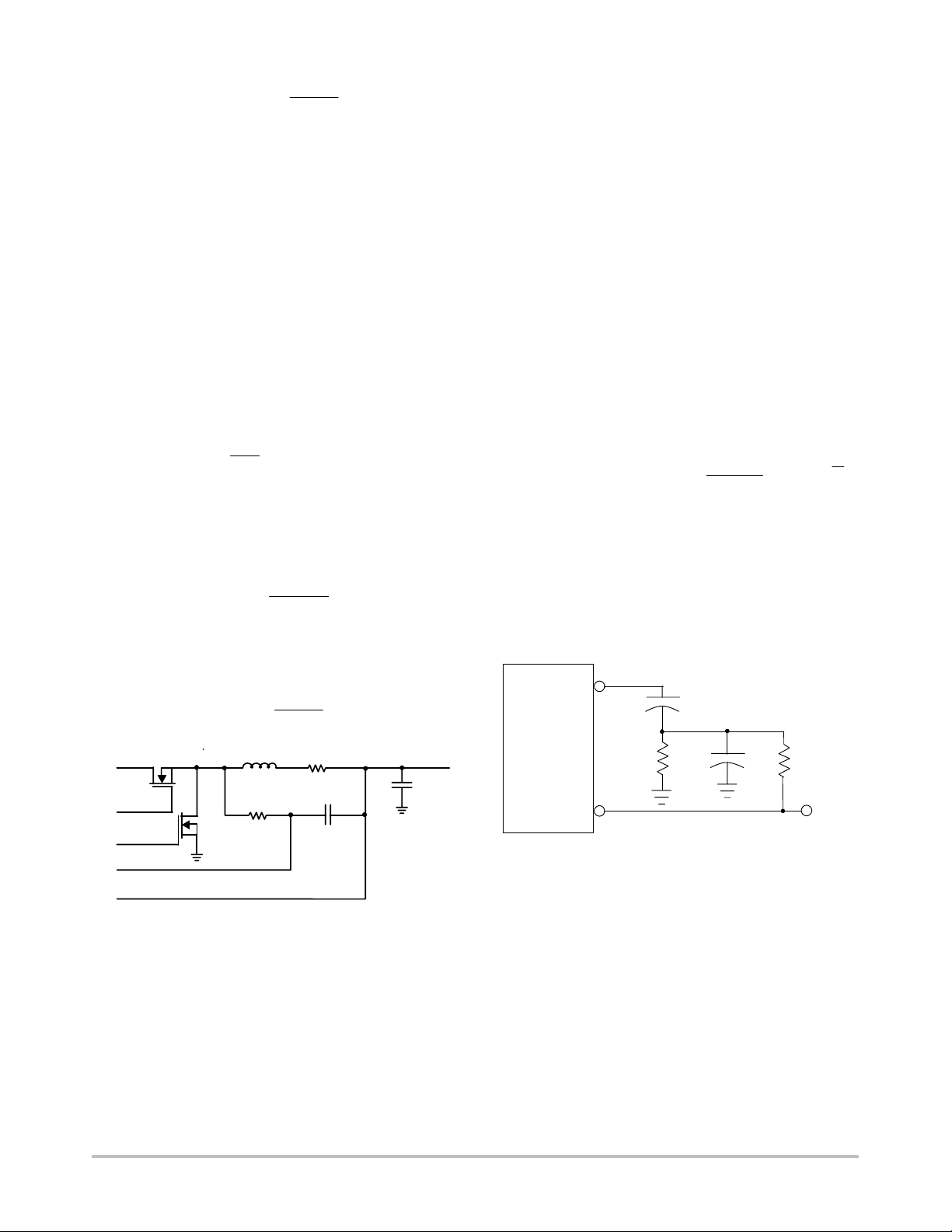
Inductor ESR. Another means of sensing current is to use
the intrinsic resistance of the inductor. A model of an
inductor reveals that the windings of an inductor have an
effective series resistance (ESR).
The voltage drop across the inductor ESR can be
measured with a simple parallel circuit: an RC integrator. I f
the value of R
and C are chosen such that:
S1
L
RS1C
ESR
then the voltage measured across the capacitor C will be:
VC ESR I
Selecting Components.
value of 0.1 µF is recommended. The value of R
LIM
Select the capacitor C first. A
can be
S1
selected according to:
ESR C
1
R
S1
Typical values for inductor ESR range in the low m;
consult manufacturer’s datasheet for specific details.
Selection of components at these values will result in a
current limit of:
LIM
0.070 V
ESR
I
current limit. Finally, one or two more components are
required for this approach than with resistor sensing.
Adding External Slope Compensation
Today’s voltage regulators are expected to meet very
stringent load transient requirements. One of the key factors
in achieving tight dynamic voltage regulation is low ESR.
Low ESR at the regulator output results in low output
voltage ripple. The consequence is, however, that very little
voltage ramp exists at the control IC feedback pin (V
FB
resulting in increased regulator sensitivity to noise and the
potential for loop instability. In applications where the
internal slope compensation is insufficient, the performance
of the NCP5424-based regulator can be improved through
the addition of a fixed amount of external slope
compensation at the output of the PWM Error Amplifier (the
COMP pin) during the regulator off-time. Referring to
Figure 8, the amount of voltage ramp at the COMP pin is
dependent on the gate voltage of the lower (synchronous)
FET and the value of resistor divider formed by R1and R2.
V
SLOPECOMP
V
GATE(L)
R2
R1 R2
(1 e
-t
)
where:
V
SLOPECOMP
V
GATE(L)
= amount of slope added;
= lower MOSFET gate voltage;
R1, R2 = voltage divider resistors;
t = tON or t
(switch off-time);
OFF
τ = RC constant determined by C1 and the parallel
combination of R1, R2 neglecting the low driver
output impedance.
COMP
C
COMP
),
L
V
CC
GATE(H)
GATE(L)
IS+
IS-
Figure 9. Inductor ESR Current Sensing
RS1
ESR
C
Co
Given an ESR value of 3.5 mΩ, the current limit becomes
20 A. If an increased current limit is required, a resistor
divider can be added.
The advantages of setting the current limit by using the
winding resistance of the inductor are that efficiency is
maximized and heat generation is minimized. The tolerance
of the inductor ESR must be factored into the design of the
http://onsemi.com
NCP5424
GATE(L)
Figure 10. Small RC Filter Provides the
Proper Voltage Ramp at the Beginning of
Each On-Time Cycle
R2
C1
R1
To Synchronous
FET
The artificial voltage ramp created by the slope
compensation scheme results in improved control loop
stability provided that the RC filter time constant is smaller
than the off-time cycle duration (time during which the
lower MOSFET is conducting). It is important that the series
combination of R1 and R2 is high enough in resistance to
avoid loading the GATE(L) pin. Also, C1 should be very
small (less than a few nF) to avoid heating the part.
17
Page 18

NCP5424
EMI MANAGEMENT
As a consequence of large currents being turned on and off
at high frequency, switching regulators generate noise as a
consequence of their normal operation. When designing for
compliance with EMI/EMC regulations, additional
components may be added to reduce noise emissions. These
components are not required for regulator operation and
experimental results may allow them to be eliminated. The
input filter inductor may not be required because bulk filter
and bypass capacitors, as well as other loads located on the
board will tend to reduce regulator di/dt effects on the circuit
board and input power supply. Placement of the power
component to minimize routing distance will also help to
reduce emissions.
LAYOUT GUIDELINES
When laying out the CPU buck regulator on a printed
circuit board, the following checklist should be used to
ensure proper operation of the NCP5424.
1. Rapid changes in voltage across parasitic capacitors
and abrupt changes in current in parasitic inductors
are major concerns for a good layout.
2. Keep high currents out of sensitive ground
connections.
3. Avoid ground loops as they pick u p noise. Use star or
single point grounding.
4. For high power buck regulators on double-sided
PCB’s a single ground plane (usually the bottom) is
recommended.
5. Even though double sided PCB’s are usually
sufficient for a good layout, four-layer PCB’s are the
optimum approach to reducing susceptibility to
noise. Use the two internal layers as the power and
GND planes, the top layer for power connections and
component vias, and the bottom layers for the noise
sensitive traces.
6. Keep the inductor switching node small by placing
the output inductor, switching and synchronous FETs
close together.
7. The MOSFET gate traces to the IC must be short,
straight, and wide as possible.
8. Use fewer, but larger output capacitors, keep the
capacitors clustered, and use multiple layer traces
with heavy copper to keep the parasitic resistance
low.
9. Place the switching MOSFET as close to the input
capacitors as possible.
10. Place the output capacitors as close to the load as
possible.
11. Place the COMP capacitor as close as possible to the
COMP pin.
12. Connect the filter components of the following pins:
R
OSC,
VFB, V
, and COMP to the GND pin with a
OUT
single trace, and connect this local GND trace to the
output capacitor GND.
13. Place the VCC bypass capacitors as close as possible
to the IC.
14. Place the R
R
pin.
OSC
resistor as close as possible to the
OSC
15. Include provisions for 100-100pF capacitor across
each resistor of the feedback network to improve
noise immunity and add COMP.
16. Assign the output with lower duty cycle to channel 2,
which has better noise immunity .
http://onsemi.com
18
Page 19
-T-
-A-
16 9
-B-
18
G
K
C
SEATING
PLANE
D
16 PL
0.25 (0.010) A
M
S
B
T
S
NCP5424
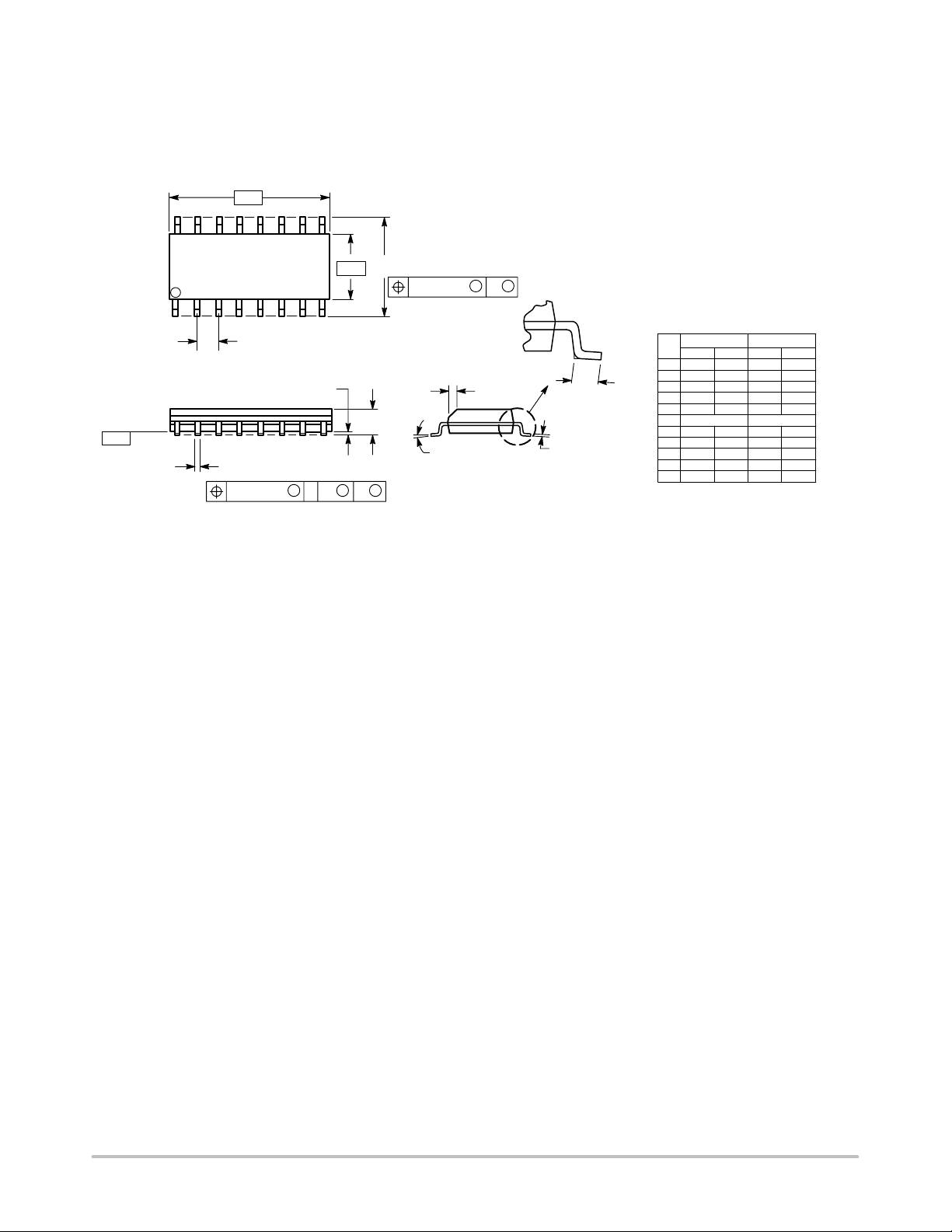
PACKAGE DIMENSIONS
SO-16
D SUFFIX
CASE 751B-05
ISSUE J
8 PLP
M
0.25 (0.010) B
M
S
X 45
R
NOTES:
1. DIMENSIONING AND TOLERANCING PER ANSI
Y14.5M, 1982.
2. CONTROLLING DIMENSION: MILLIMETER.
3. DIMENSIONS A AND B DO NOT INCLUDE
MOLD PROTRUSION.
4. MAXIMUM MOLD PROTRUSION 0.15 (0.006)
PER SIDE.
5. DIMENSION D DOES NOT INCLUDE DAMBAR
PROTRUSION. ALLOWABLE DAMBAR
PROTRUSION SHALL BE 0.127 (0.005) TOTAL
IN EXCESS OF THE D DIMENSION AT
MAXIMUM MATERIAL CONDITION.
DIM MIN MAX MIN MAX
A 9.80 10.00 0.386 0.393
F
J
B 3.80 4.00 0.150 0.157
C 1.35 1.75 0.054 0.068
D 0.35 0.49 0.014 0.019
F 0.40 1.25 0.016 0.049
G 1.27 BSC 0.050 BSC
J 0.19 0.25 0.008 0.009
K 0.10 0.25 0.004 0.009
M 0 7 0 7
P 5.80 6.20 0.229 0.244
R 0.25 0.50 0.010 0.019
INCHESMILLIMETERS
http://onsemi.com
19
Page 20
NCP5424
V2 is a trademark of Switch Power, Inc.
ON Semiconductor and are registered trademarks of Semiconductor Components Industries, LLC (SCILLC). SCILLC reserves the right to make
changes without further notice to any products herein. SCILLC makes no warranty, representation or guarantee regarding the suitability of its products for any
particular purpose, nor does SCILLC assume any liability arising out of the application or use of any product or circuit, and specifically disclaims any and all
liability, including without limitation special, consequential or incidental damages. “Typical” parameters which may be provided in SCILLC data sheets and/or
specifications can and do vary in different applications and actual performance may vary over time. All operating parameters, including “Typicals” must be
validated for each customer application by customer’s technical experts. SCILLC does not convey any license under its patent rights nor the rights of others.
SCILLC products are not designed, intended, or authorized for use as components in systems intended for surgical implant into the body, or other applications
intended to support or sustain life, or for any other application in which the failure of the SCILLC product could create a situation where personal injury or death
may occur. Should Buyer purchase or use SCILLC products for any such unintended or unauthorized application, Buyer shall indemnify and hold SCILLC
and its officers, employees, subsidiaries, affiliates, and distributors harmless against all claims, costs, damages, and expenses, and reasonable attorney fees
arising out of, directly or indirectly, any claim of personal injury or death associated with such unintended or unauthorized use, even if such claim alleges that
SCILLC was negligent regarding the design or manufacture of the part. SCILLC is an Equal Opportunity/Affirmative Action Employer.
PUBLICATION ORDERING INFORMATION
Literature Fulfillment:
Literature Distribution Center for ON Semiconductor
P.O. Box 5163, Denver, Colorado 80217 USA
Phone: 303-675-2175 or 800-344-3860 Toll Free USA/Canada
Fax: 303-675-2176 or 800-344-3867 Toll Free USA/Canada
Email: [email protected]
N. American Technical Support: 800-282-9855 Toll Free USA/Canada
http://onsemi.com
JAPAN: ON Semiconductor, Japan Customer Focus Center
2-9-1 Kamimeguro, Meguro-ku, Tokyo, Japan 153-0051
Phone: 81-3-5773-3850
ON Semiconductor Website: http://onsemi.com
For additional information, please contact your local
Sales Representative.
NCP5424/D
20
 Loading...