

Page 1

NCP5392
www.BDTIC.com/ON
2/3/4-Phase Controller for
CPU Applications
The NCP5392 provides up to a four−phase buck solution which
combines differential voltage sensing, differential phase current
sensing, and adaptive voltage positioning to provide accurately
regulated power for both Intel and AMD processors. Dual−edge
pulse−width modulation (PWM) combined with inductor current
sensing reduces system cost by providing the fastest initial response
to dynamic load events. Dual−edge multiphase modulation reduces
the total bulk and ceramic output capacitance required to meet
transient regulation specifications.
A high performance operational error amplifier is provided to
simplify compensation of the system. Dynamic Reference Injection
further simplifies loop compensation by eliminating the need to
compromise between closed−loop transient response and Dynamic
VID performance.
Features
• Meets Intel’s VR11.1 Specifications
• Meets AMD 6 Bit Code Specifications
• Dual−edge PWM for Fastest Initial Response to Transient Loading
• High Performance Operational Error Amplifier
• Internal Soft Start
• Dynamic Reference Injection
• DAC Range from 0.375 V to 1.6 V
• DAC Feed Forward (Patent Pending)
• ±0.5% DAC Voltage Accuracy from 1.0 V to 1.6 V
• True Differential Remote Voltage Sensing Amplifier
• Phase−to−Phase Current Balancing
• “Lossless” Differential Inductor Current Sensing
• Differential Current Sense Amplifiers for each Phase
• Adaptive Voltage Positioning (AVP)
• Oscillator Frequency Range of 100 kHz – 1 MHz
• Latched Over Voltage Protection (OVP)
• Guaranteed Startup into Pre−Charged Loads
• Threshold Sensitive Enable Pin for VTT Sensing
• Power Good Output with Internal Delays
• Thermally Compensated Current Monitoring
• This is a Pb−Free Device
®
(Patent #US07057381)
http://onsemi.com
MARKING
DIAGRAM
1
401
40 PIN QFN, 6x6
MN SUFFIX
CASE 488AR
NCP5392 = Specific Device Code
A = Assembly Location
WL = Wafer Lot
YY = Year
WW = Work Week
G = Pb−Free Package
*Pin 41 is the thermal pad on the bottom of the device.
ORDERING INFORMATION
Device Package Shipping
NCP5392MNR2G* QFN−40
(Pb−Free)
*Temperature Range: 0°C to 85°C
†For information on tape and reel specifications,
including part orientation and tape sizes, please
refer to our Tape and Reel Packaging Specification
Brochure, BRD8011/D.
NCP5392
AWLYYWWG
2500/Tape & Reel
†
Applications
• Desktop Processors
© Semiconductor Components Industries, LLC, 2008
August, 2008 − Rev. 3
1 Publication Order Number:
NCP5392/D
Page 2
NCP5392
www.BDTIC.com/ON
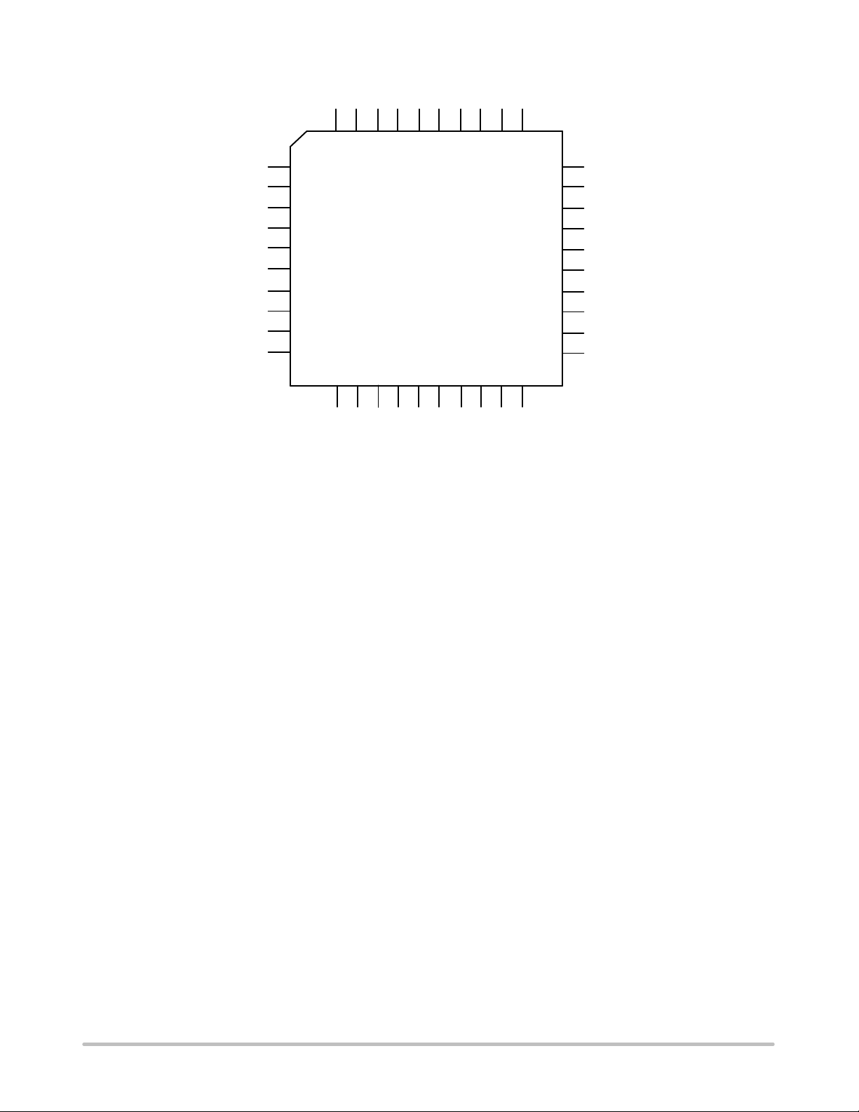
PIN CONNECTIONS
40
39
38
37
36
35
34G433G332G231
PSI
NTC
DAC
1
EN
2
VID0
3
VID1
4
VID2
5
VID3
6
VID4
7
VID5
8
VID6
9
VID7
10
ROSC
VR_HOT
VR_RDY
2/3/4−Phase Buck Controller
ILIM11IMON12VSP13VSN14DIFFOUT15COMP16VFB17VDRP18VDFB19CSSUM
VCC
12VMON
DRVON
NCP5392
(QFN40)
20
Figure 1. NCP5392 QFN40 Pin Connections (Top View)
CS4
CS4N
CS3
CS3N
CS2
CS2N
CS1
CS1N
G1
30
29
28
27
26
25
24
23
22
21
http://onsemi.com
2
Page 3
VID0
www.BDTIC.com/ON
VID1
VID2
VID3
VID4
VID5
VID6
VID7/AMD
DAC
NCP5392
Flexible DAC
Overvoltage
Protection
−
+
VSN
VSP
DIFFOUT
VFB
COMP
VDRP
VDFB
CSSUM
CS1P
CS1N
CS2P
CS2N
CS3P
CS3N
CS4P
CS4N
ROSC
ILIM
EN
VCC
+
1.3 V
+
−
+
−
+
−
+
−
+
−
Oscillator
−
+
Diff Amp
+
−
Droop Amp
−2/3
Gain = 6
Gain = 6
Gain = 6
Gain = 6
Error Amp
+
+
4.25 V
+
+
+
+
−
UVLO
+
−
+
−
+
−
+
+
+
−
+
−
ILimit
Control,
Fault Logic
and
Monitor
Circuits
G1
G2
G3
G4
IMON
DRVON
PSI
NTC
VR_HOT
12VMON
VR_RDY
GND (FLAG)
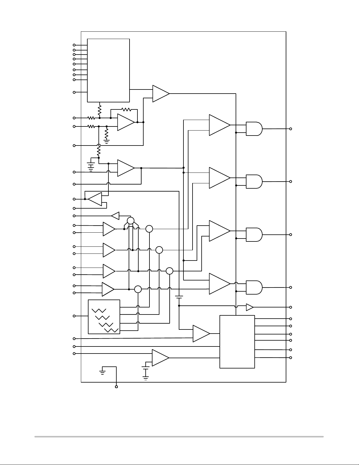
Figure 2. NCP5392 Block Diagram
http://onsemi.com
3
Page 4
NCP5392
www.BDTIC.com/ON
VTT
RFB
CFB1
CF
RDRP
RISO1 RISO2RT2
RFB1
RF
CH
RNOR
CDFB
12V_FILTER
2
3
4
5
6
7
8
9
1
39
40
14
13
15
16
17
18
19
R6R6
20
36
CDNI
RDNP
+5V
VID0
VID1
VID2
VID3
VID4
VID5
VID6
VID7
EN
VR_RDY
VR_HOT
VSN
VSP
DIFFOUT
COMP
VFB
VDRP
VDFB
CSSUM
DAC
41 11 10
12VMON
NCP5392
GND
VCC
ILIM
373534
NTC
IMON
G1
CS1P
CS1N
G2
CS2P
CS2N
G3
CS3P
CS3N
G4
CS4P
CS4N
DRVON
ROSC
RLIM1
RLIM2
12V_FILTER12V_FILTER
D1
C4
C3
PSI
3812PSI
IMON
30
22
21
31
24
23
32
26
25
33
28
27
29
C1
RNTC1
RT1
VCC
NCP5359
OD
IN
VCC
NCP5359
OD
IN
VCC
NCP5359
OD
IN
BST
DRH
SW
DRL
PGND
BST
DRH
SW
DRL
PGND
BST
DRH
SW
DRL
PGND
12V_FILTER12V_FILTER
12V_FILTER12V_FILTER
Q1
Q2 R2 RS1
C2
L1
CS1
+
CPU GND
BST
VCC
DRH
NCP5359
SW
OD
DRL
IN
PGND
VCCP
VSSN
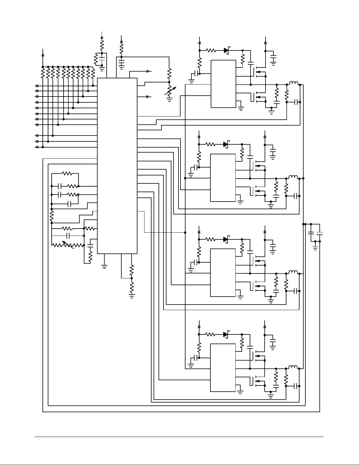
Figure 3. Application Schematic for Four Phases
http://onsemi.com
4
12V_FILTER12V_FILTER
Page 5
NCP5392
www.BDTIC.com/ON
VTT
RFB
CFB1
CF
RDRP
RISO1 RISO2RT2
RFB1
RF
CH
RNOR
CDFB
12V_FILTER
2
3
4
5
6
7
8
9
1
39
40
14
13
15
16
17
18
19
R6R6
20
36
CDNI
RDNP
+5V
VID0
VID1
VID2
VID3
VID4
VID5
VID6
VID7
EN
VR_RDY
VR_HOT
VSN
VSP
DIFFOUT
COMP
VFB
VDRP
VDFB
CSSUM
DAC
41 11 10
12VMON
NCP5392
GND
VCC
ILIM
373534
NTC
IMON
G1
CS1P
CS1N
G2
CS2P
CS2N
G3
CS3P
CS3N
G4
CS4P
CS4N
DRVON
ROSC
RLIM1
RLIM2
12V_FILTER12V_FILTER
D1
C4
C3
PSI
3812PSI
IMON
30
22
21
31
24
23
32
26
25
33
28
27
29
RNTC1
RT1
C1
VCC
NCP5359
OD
IN
VCC
NCP5359
OD
IN
VCC
NCP5359
OD
IN
BST
DRH
SW
DRL
PGND
BST
DRH
SW
DRL
PGND
BST
DRH
SW
DRL
PGND
Q1
L1
Q2
12V_FILTER12V_FILTER
12V_FILTER12V_FILTER
RS1R2
C2
CS1
+
CPU GND
VCCP
VSSN
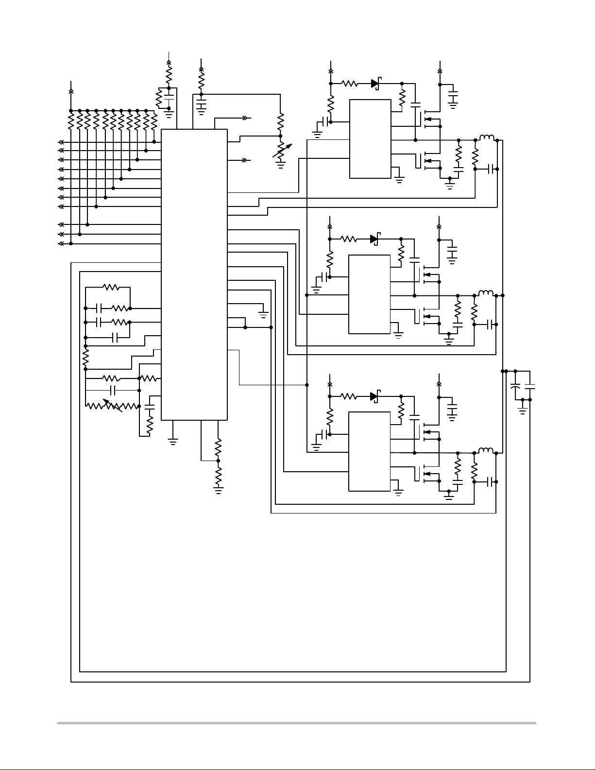
Figure 4. Application Schematic for Three Phases
http://onsemi.com
5
Page 6
NCP5392
www.BDTIC.com/ON
VTT
RFB
CFB1
CF
RDRP
RISO1 RISO2RT2
RFB1
RF
CH
RNOR
CDFB
12V_FILTER
2
3
4
5
6
7
8
9
1
39
40
14
13
15
16
17
18
19
R6R6
20
36
CDNI
RDNP
+5V
VID0
VID1
VID2
VID3
VID4
VID5
VID6
VID7
EN
VR_RDY
VR_HOT
VSN
VSP
DIFFOUT
COMP
VFB
VDRP
VDFB
CSSUM
DAC
41 11 10
12VMON
NCP5392
GND
VCC
ILIM
373534
NTC
IMON
G1
CS1P
CS1N
G2
CS2P
CS2N
G3
CS3P
CS3N
G4
CS4P
CS4N
DRVON
ROSC
RLIM1
RLIM2
12V_FILTER12V_FILTER
D1
C4
C3
PSI
3812PSI
IMON
30
22
21
31
24
23
32
26
25
33
28
27
29
RNTC1
RT1
C1
VCC
NCP5359
OD
IN
VCC
NCP5359
OD
IN
BST
DRH
SW
DRL
PGND
BST
DRH
SW
DRL
PGND
Q1
L1
Q2
12V_FILTER12V_FILTER
RS1R2
C2
CS1
+
CPU GND
VCCP
VSSN
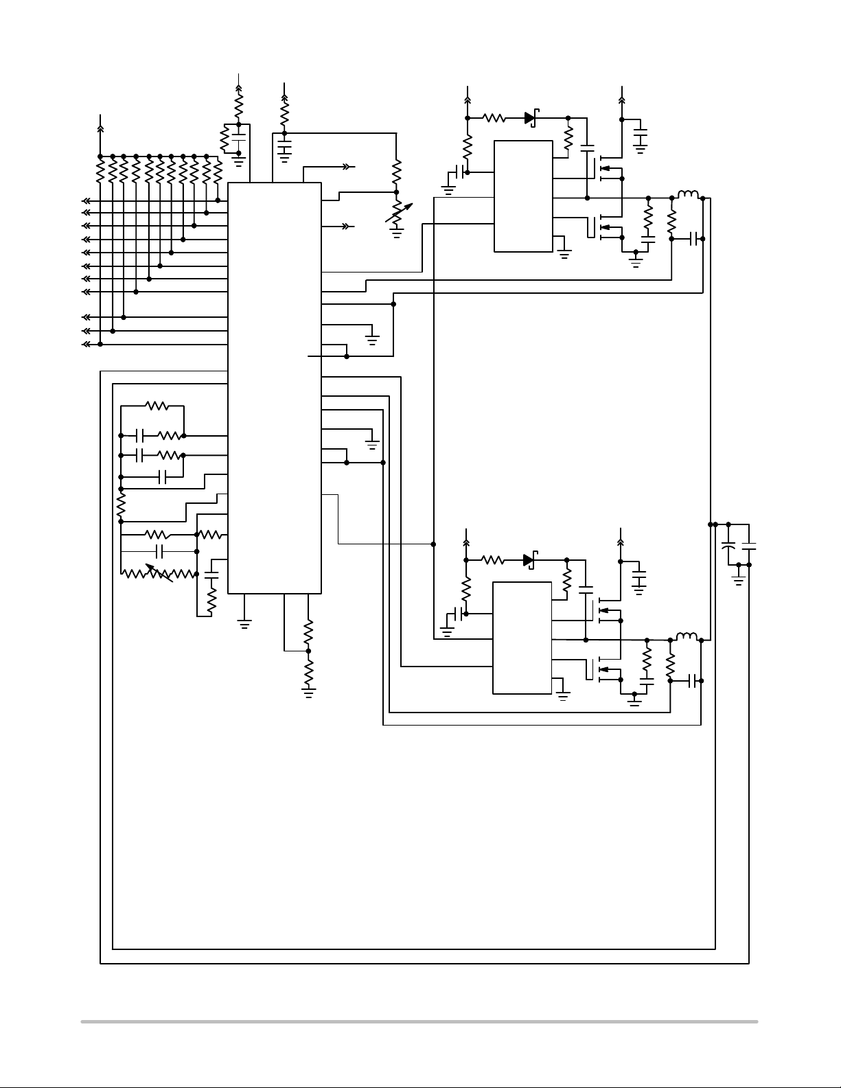
Figure 5. Application Schematic for Two Phases
http://onsemi.com
6
Page 7

NCP5392
www.BDTIC.com/ON
PIN DESCRIPTIONS
Pin No. Symbol Description
1 EN Threshold sensitive input. High = startup, Low = shutdown.
2 VID0 Voltage ID DAC input
3 VID1 Voltage ID DAC input
4 VID2 Voltage ID DAC input
5 VID3 Voltage ID DAC input
6 VID4 Voltage ID DAC input
7 VID5 Voltage ID DAC input
8 VID6 Voltage ID DAC input
9 VID7/AMD Voltage ID DAC input. Pull to VCC (5 V) to enable AMD 6−bit DAC code.
10 ROSC A resistance from this pin to ground programs the oscillator frequency according to fSW. This pin supplies a
11 ILIM Overcurrent shutdown threshold setting. Connect this pin to the ROSC pin via a resistor divider as shown in
12 IMON 0 mV to 900 mV analog signal proportional to the output load current. VSN referenced
13 VSP Non−inverting input to the internal differential remote sense amplifier
14 VSN Inverting input to the internal differential remote sense amplifier
15 DIFFOUT Output of the differential remote sense amplifier
16 COMP Output of the error amplifier
17 VFB Compensation Amplifier Voltage feedback
18 VDRP Voltage output signal proportional to current used for current limit and output voltage droop
19 VDFB Droop Amplifier Voltage Feedback
20 CSSUM Inverted Sum of the Differential Current Sense inputs. Av=CSSUM/CSx = −4
21 CS1N Inverting input to current sense amplifier #1
22 CS1 Non−inverting input to current sense amplifier #1
23 CS2N Inverting input to current sense amplifier #2
24 CS2 Non−inverting input to current sense amplifier #2
25 CS3N Inverting input to current sense amplifier #3
26 CS3 Non−inverting input to current sense amplifier #3
27 CS4N Inverting input to current sense amplifier #4
28 CS4 Non−inverting input to current sense amplifier #4
29 DRVON Bidirectional Gate Drive Enable
30 G1 PWM output pulse to gate driver. 3−level output: Low = LSFET Enabled, Mid = Diode Emulation Enabled,
31 G2 PWM output pulse to gate driver. 3−level output (see G1)
32 G3 PWM output pulse to gate driver. 3−level output (see G1)
33 G4 PWM output pulse to gate driver. 3−level output (see G1)
34 12VMON Monitor a 12 V input through a resistor divider.
35 VCC Power for the internal control circuits.
36 DAC DAC Feed Forward Output
37 PSI Power Saving Control. Low = single phase operation, High = normal operation.
38 NTC Threshold sensitive input for thermal monitoring
39 VR_RDY Open collector output. High indicates that the output is regulating
40 VR_HOT Open collector output indicates the state of the thermal monitoring input. Low impedance output indicating a
FLAG GND Power supply return (QFN Flag)
trimmed output voltage of 2 V.
the Application Schematics. To disable the overcurrent feature, connect this pin directly to the ROSC pin. To
guarantee correct operation, this pin should only be connected to the voltage generated by the ROSC pin; do
not connect this pin to any externally generated voltages.
High = HSFET Enabled
normal status when the voltage of NTC pin is above the specified threshold. This pin will transition to high
impedance when the voltage of NTC pin decrease (temperature increase) below the specified threshold.
This pin requires an external pullup resistor
http://onsemi.com
7
Page 8
NCP5392
www.BDTIC.com/ON
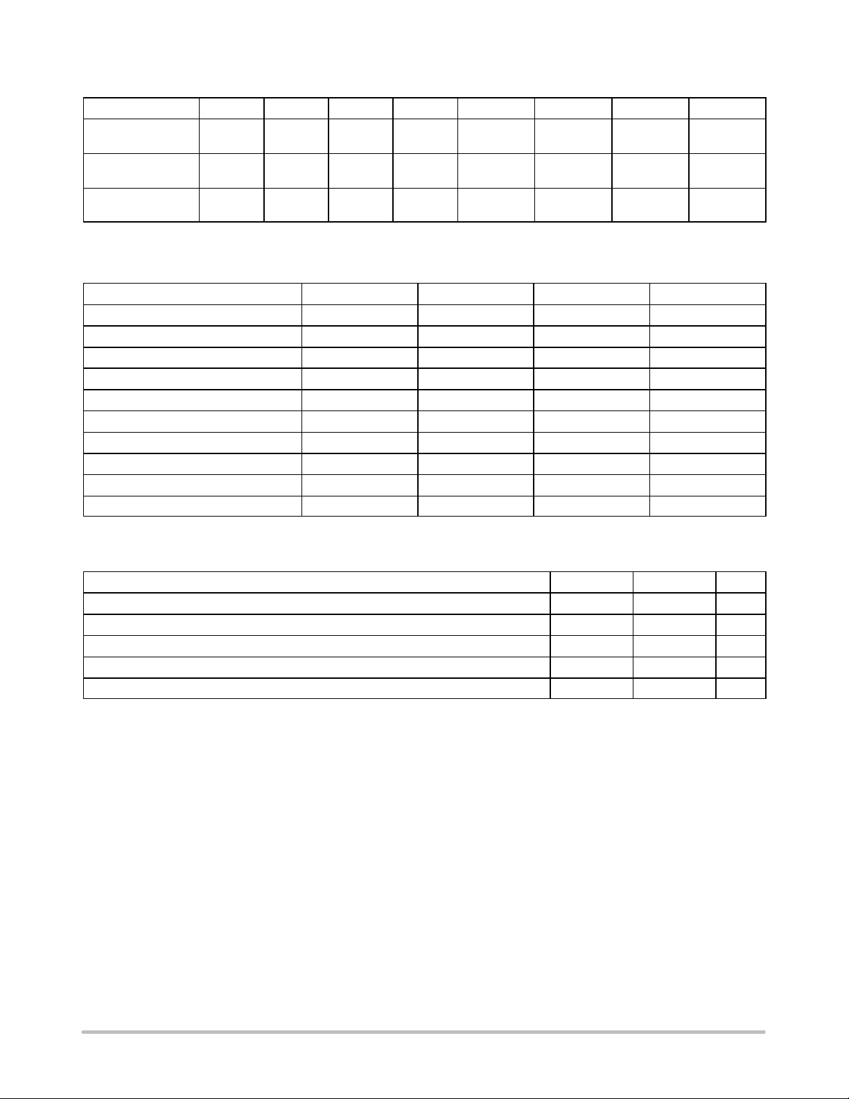
PIN CONNECTIONS VS. PHASE COUNT
Number of Phases G4 G3 G2 G1 CS4−CS4N CS3−CS3N CS2−CS2N CS1−CS1N
4 Phase 4
3 Tie to
2 Tie to
Out
GND
GND
MAXIMUM RATINGS
ELECTRICAL INFORMATION
Pin Symbol V
COMP 5.5 V −0.3 V 10 mA 10 mA
V
DRP
V+ 5.5 V GND – 300 mV 1 mA 1 mA
V– GND + 300 mV GND – 300 mV 1 mA 1 mA
DIFFOUT 5.5 V −0.3 V 20 mA 20 mA
VR_RDY 5.5 V −0.3 V N/A 20 mA
VCC 7.0 V −0.3 V N/A 10 mA
ROSC 5.5 V −0.3 V 1 mA N/A
IMON Output 1.1 V
All Other Pins 5.5 V −0.3 V
*All signals referenced to AGND unless otherwise noted.
Phase 3
Out
Phase 3
Out
Phase 2
Out
Phase 2
Out
Phase 2
Out
Tie to
GND
MAX
5.5 V −0.3 V 5 mA 5 mA
Phase 1
Out
Phase 1
Out
Phase 1
Out
Phase 4 CS
input
Tie to
VCCP
Tie to
VCCP
V
MIN
Phase 3 CS
input
Phase 3 CS
input
Phase 2 CS
input
I
SOURCE
Phase 2 CS
input
Phase 2 CS
input
Tie to
VCCP
I
Phase 1 CS
input
Phase 1 CS
input
Phase 1 CS
input
SINK
THERMAL INFORMATION
Rating Symbol Value Unit
Thermal Characteristic, QFN Package (Note 1) R
Operating Junction Temperature Range (Note 2) T
Operating Ambient Temperature Range T
Maximum Storage Temperature Range T
Moisture Sensitivity Level, QFN Package MSL 1
Stresses exceeding Maximum Ratings may damage the device. Maximum Ratings are stress ratings only. Functional operation above the
Recommended Operating Conditions is not implied. Extended exposure to stresses above the Recommended Operating Conditions may affect
device reliability.
*The maximum package power dissipation must be observed.
1. JESD 51−5 (1S2P Direct−Attach Method) with 0 LFM.
2. JESD 51−7 (1S2P Direct−Attach Method) with 0 LFM.
JA
J
A
STG
34 °C/W
0 to 125 °C
0 to +85 °C
−55 to +150 °C
http://onsemi.com
8
Page 9
NCP5392
www.BDTIC.com/ON
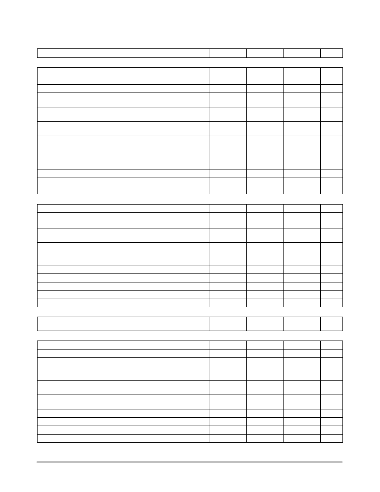
ELECTRICAL CHARACTERISTICS
(Unless otherwise stated: 0°C < T
Parameter Test Conditions Min Typ Max Unit
ERROR AMPLIFIER
Input Bias Current (Note 3) −200 200 nA
Noninverting Voltage Range (Note 3) 0 1.3 3 V
Input Offset Voltage (Note 3) V+ = V− = 1.1 V −1.0 − 1.0 mV
Open Loop DC Gain CL = 60 pF to GND,
Open Loop Unity Gain Bandwidth CL = 60 pF to GND,
Open Loop Phase Margin CL = 60 pF to GND,
Slew Rate Vin = 100 mV, G = − 10 V/V,
Maximum Output Voltage I
Minimum Output Voltage I
Output source current (Note 3) V
Output sink current (Note 3) V
DIFFERENTIAL SUMMING AMPLIFIER
VSN Input Bias Current VSN Voltage = 0 V 30 A
VSP Input Resistance DRVON = Low
VSP Input Bias Voltage DRVON = Low
Input Voltage Range (Note 3) −0.3 − 3.0 V
−3 dB Bandwidth CL = 80 pF to GND,
Closed Loop DC Gain VS to Diffout VS+ to VS− = 0.5 to 1.6 V 0.98 1.0 1.025 V/V
Maximum Output Voltage I
Minimum Output Voltage I
Output source current (Note 3) V
Output sink current (Note 3) V
INTERNAL OFFSET VOLTAGE
Offset Voltage to the (+) Pin of the
Error Amp and the VDRP pin
VDROOP AMPLIFIER
Input Bias Current (Note 3) −200 200 nA
Non−inverting Voltage Range (Note 3) 0 1.3 3 V
Input Offset Voltage (Note 3) V+ = V− = 1.1 V −4.0 − 4.0 mV
Open Loop DC Gain CL = 20 pF to GND including
Open Loop Unity Gain Bandwidth CL = 20 pF to GND including
Slew Rate CL = 20 pF to GND including
Maximum Output Voltage I
Minimum Output Voltage I
Output source current (Note 3) V
Output sink current (Note 3) V
3. Guaranteed by design, not tested in production.
< 85°C; 4.75 V < VCC < 5.25 V; All DAC Codes; C
A
RL = 10 K to GND
RL = 10 K to GND
RL = 10 K to GND
V
= 1.5 V – 2.5 V,
out
CL = 60 pF to GND,
DC Load = ±125 A to GND
= 2.0 mA 3.5 − − V
SOURCE
= 0.2 mA − − 50 mV
SINK
= 3.5 V 2 − − mA
out
= 1.0 V 2 − − mA
out
DRVON = High
DRVON = High
RL = 10 K to GND
= 2 mA 3.0 − − V
SOURCE
= 2 mA − − 0.5 V
SINK
= 3 V 2.0 − − mA
out
= 0.5 V 2.0 − − mA
out
ESD, RL = 1 k to GND
ESD, RL = 1 k to GND
ESD, RL = 1 k to GND
= 4.0 mA 3 − − V
SOURCE
= 1.0 mA − − 1 V
SINK
= 3.0 V 4 − − mA
out
= 1.0 V 1 − − mA
out
= 0.1 F)
VCC
− 100 dB
− 10 − MHz
− 80 − °
− 5 − V/s
1.5
17
0.09
0.66
− 10 − MHz
− 1.30 − V
− 100 dB
− 10 − MHz
− 5 − V/s
k
V
http://onsemi.com
9
Page 10
NCP5392
www.BDTIC.com/ON
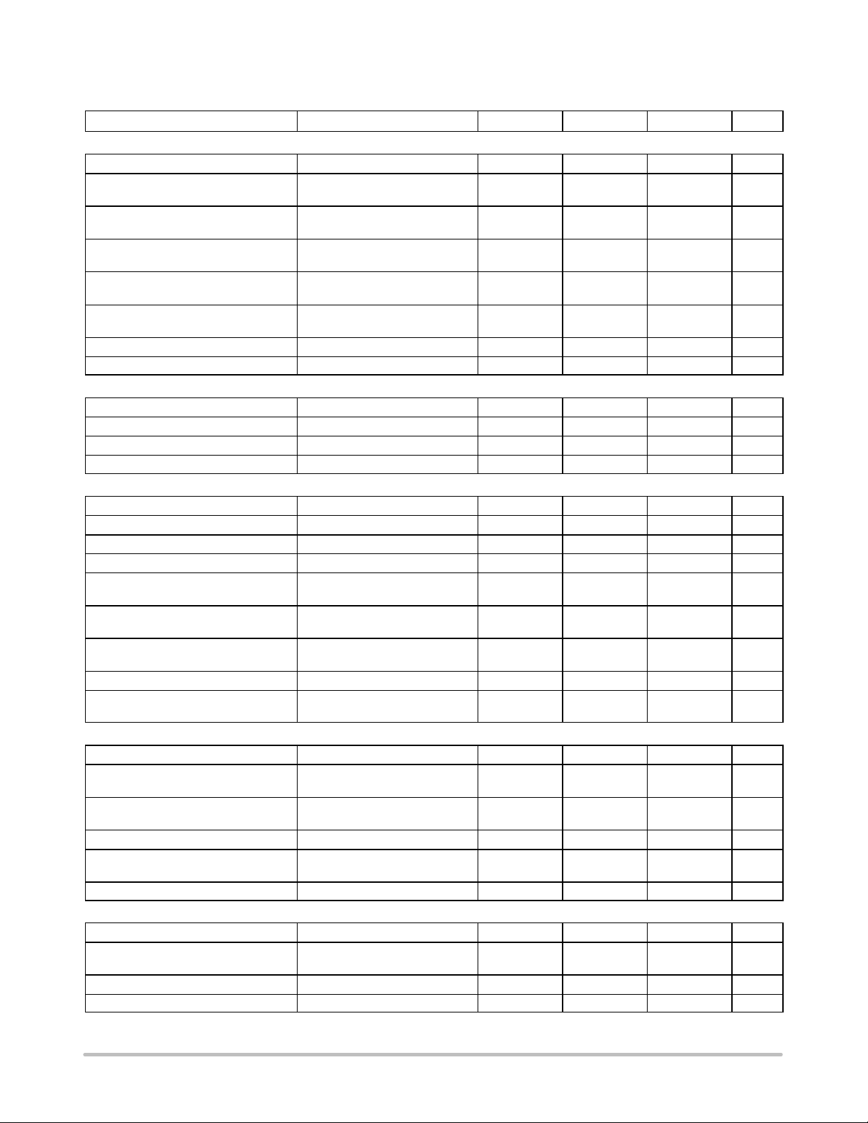
ELECTRICAL CHARACTERISTICS
(Unless otherwise stated: 0°C < T
Parameter UnitMaxTypMinTest Conditions
CSSUM AMPLIFIER
Current Sense Input to CSSUM Gain −60 mV < CS < 60 mV −4.00 −3.88 −3.76 V/V
Current Sense Input to CSSUM −3 dB
Bandwidth
Current Sense Input to CSSUM
Output Slew Rate
Current Summing Amp Output Offset
Voltage
Maximum CSSUM Output Voltage CSx – CSxN = −0.15 V
Minimum CSSUM Output Voltage CSx – CSxN = 0.066 V
Output source current (Note 3) V
Output sink current (Note 3) V
PSI (Power Saving Control, Active Low)
Enable High Input Leakage Current External 1 K Pullup to 3.3 V − − 1.0 A
Upper Threshold V
Lower Threshold V
Hysteresis V
DRVON
Output High Voltage Sourcing 500 A 3.0 − − V
Sourcing Current for Output High VCC = 5 V − 2.5 4.0 mA
Output Low Voltage Sinking 500 A − − 0.7 V
Sinking Current for Output Low 2.5 − − mA
Delay Time Propagation Delay from EN Low
Rise Time CL (PCB) = 20 pF, Vo = 10% to
Fall Time CL (PCB) = 20 pF, Vo = 10% to
Internal Pulldown Resistance 35 70 140 k
VCC Voltage when DRVON
Output Valid
CURRENT SENSE AMPLIFIERS
Input Bias Current (Note 3) CSx = CSxN = 1.4 V − 0 − nA
Common Mode Input Voltage Range
(Note 3)
Differential Mode Input Voltage Range
(Note 3)
Input Offset Voltage CSx = CSxN = 1.1 V, −1.0 − 1.0 mV
Current Sense Input to PWM Gain
(Note 3)
Current Sharing Offset CS1 to CSx All VID codes −2.5 − 2.5 mV
IMON
V
to IMON Gain 1.325 V< V
DRP
V
to IMON −3 dB Bandwidth CL = 30 pF to GND,
DRP
Output Referred Offset Voltage V
Minimum Output Voltage V
3. Guaranteed by design, not tested in production.
< 85°C; 4.75 V < VCC < 5.25 V; All DAC Codes; C
A
CL = 10 pF to GND,
R
= 10 k to GND
L
Vin = 25 mV, CL = 10 pF to
GND, Load = 1 k to 1.3 V
CSx – CSNx = 0, CSx = 1.1 V −15 − +15 mV
(All Phases) I
(All Phases) I
= 3.0 V 1 − − mA
out
= 0.3 V 1 − − mA
out
UPPER
LOWER
− V
UPPER
to DRVON
90%
90%
0 V < CSx − CSxN < 0.1 V, 5.7 6.0 6.3 V/V
RL = 100 k to GND
DRP
DRP
LOWER
DRP
= 1.6 V, I
= 1.2 V, I
= 1 mA
SOURCE
= 1 mA
SINK
< 1.8 V 1.98 2 2.02 V/V
= 0 mA 81 90 99 mV
SOURCE
= 100 A − − 0.11 V
SINK
= 0.1 F)
VCC
− 4 − MHz
− 4 − V/s
3.0 − − V
− − 0.3 V
− 650 770 mV
450 550 − mV
− 100 − mV
− 10 − ns
− 130 − ns
− 10 − ns
− − 2.0 V
−0.3 − 2.0 V
−120 − 120 mV
− 4 MHz
http://onsemi.com
10
Page 11
NCP5392
www.BDTIC.com/ON
ELECTRICAL CHARACTERISTICS
(Unless otherwise stated: 0°C < T
Parameter UnitMaxTypMinTest Conditions
IMON
Output source current (Note 3) V
Output sink current (Note 3) V
Maximum Clamp Voltage V
OSCILLATOR
Switching Frequency Range (Note 3) 100 − 1000 kHz
Switching Frequency Accuracy 2− or
4−Phase
Switching Frequency Accuracy
3−Phase
R
Output Voltage 1.95 2.01 2.065 V
OSC
MODULATORS (PWM Comparators)
Minimum Pulse Width FSW = 800 KHz − 30 − ns
Propagation Delay ±20 mV of Overdrive − 10 − ns
0% Duty Cycle COMP Voltage when the PWM
100% Duty Cycle COMP Voltage when the PWM
PWM Ramp Duty Cycle Matching Between Any Two Phases − 90 − %
PWM Phase Angle Error (Note 3) Between Adjacent Phases 15 − 15 °
VR_RDY (POWER GOOD) OUTPUT
VR_RDY Output Saturation Voltage I
VR_RDY Rise Time (Note 3) External Pullup of 1 k to 1.25
VR_RDY Output Voltage at Powerup
(Note 3)
VR_RDY High – Output Leakage
Current (Note 3)
VR_RDY Upper Threshold Voltage VCore Increasing, DAC = 1.3 V − 310 270 mV
VR_RDY Lower Threshold Voltage VCore Decreasing
VR_RDY Rising Delay VCore Increasing − 500 − s
VR_RDY Falling Delay VCore Decreasing − 5 − s
PWM OUTPUTS
Output High Voltage Sourcing 500 A 3.0 − − V
Mid Output Voltage 1.4 1.5 1.6 V
Output Low Voltage Sinking 500 A − − 0.7 V
Delay + Fall Time (Note 3) CL (PCB) = 50 pF,
Delay + Rise Time (Note 3) CL (PCB) = 50 pF,
3. Guaranteed by design, not tested in production.
< 85°C; 4.75 V < VCC < 5.25 V; All DAC Codes; C
A
= 1 V 300 − − A
out
= 0.3 V 300 − − A
out
Voltage = 2 V,
DRP
R
= 100 k
LOAD
R
= 49.9 k 200 − 224
OSC
R
= 24.9 k 374 − 414
OSC
R
= 10 k 800 − 978
OSC
R
= 49.9 k 191 − 234
OSC
R
= 24.9 k 354 − 434
OSC
R
= 10 k 755 − 1000
OSC
Outputs Remain LO
Outputs Remain HI
= 10 mA, − − 0.4 V
PGD
V, C
= 45 pF, Vo = 10% to
TOT
90%
VR_RDY Pulled up to 5 V via
2k, t
100 s ≤ t
VR_RDY = 5.5 V via 1 K − − 0.2 A
DAC = 1.3 V
Vo = VCC to GND
Vo = GND to V
R(VCC)
R(VCC)
≤ 3 x t
≤ 20 ms
CC
R(5V)
= 0.1 F)
VCC
− − 1.15 V
kHz
kHz
− 1.3 − V
− 2.3 − V
− 100 150 ns
− − 1.0 V
Below
DAC
410 370 mV
− 10 15 ns
− 10 15 ns
Below
DAC
http://onsemi.com
11
Page 12
NCP5392
www.BDTIC.com/ON
ELECTRICAL CHARACTERISTICS
(Unless otherwise stated: 0°C < T
Parameter UnitMaxTypMinTest Conditions
PWM OUTPUTS
Output Impedance – HI or LO State Resistance to VCC (HI) or GND
2/3/4−PhASE DETECTION
Gate Pin Source Current 60 80 150 A
Gate Pin Threshold Voltage 210 240 265 mV
Phase Detect Timer 15 20 27 s
DIGITAL SOFT−START
Soft−Start Ramp Time DAC = 0 to DAC = 1.1 V 1.0 − 1.5 ms
VR11 Vboot time 400 500 600 s
VID7/VR11/AMD INPUT
VID Upper Threshold V
VID Lower Threshold V
VID Hysteresis V
AMD Input Bias Current 10 − 20 A
VR11 Input Bias Current (Note 3) 200 nA
Delay before Latching VID Change
(VID De−Skewing) (Note 3)
AMD Upper Threshold (Note 3) 2.9 V
AMD Lower Threshold (Note 3) 2.4 V
ENABLE INPUT
Enable High Input Leakage Current
(Note 3)
VR11 Rising Threshold − 650 770 mV
VR11 Falling Threshold 450 550 − mV
VR11 Total Hysteresis Rising− Falling Threshold − 100 − mV
AMD Upper Threshold − 1.3 1.5 V
AMD Lower Threshold 0.9 1.1 − V
AMD Total Hysteresis Rising − Falling Threshold 200 mV
Enable Delay Time Measure Time from Enable
CURRENT LIMIT
I
I
I
I
I
LIM
LIM
LIM
LIM
LIM
to V
to V
to V
to V
Gain Between V
DRP
Gain in PSI 4 phase Between V
DRP
Gain in PSI 3 phase Between V
DRP
Gain in PSI 2 phase Between V
DRP
Offset V
Delay − 100 − ns
OVERVOLTAGE PROTECTION
VR11 Overvoltage Threshold DAC +150 DAC +185 DAC +200 mV
VR11 PSI Overvoltage Threshold
(Note 3)
AMD Overvoltage Threshold (Note 3) DAC +200 DAC +235 DAC +305 mV
3. Guaranteed by design, not tested in production.
< 85°C; 4.75 V < VCC < 5.25 V; All DAC Codes; C
A
(LO)
UPPER
LOWER
− V
UPPER
LOWER
Measured from the edge of the
1st VID change
Pullup to 1.3 V − − 200 nA
Transitioning HI to when Output
Begins
− V
= 450 mV
DRP
and V
and V
and V
and V
DRP
DRP
DRP
DRP
DRP
− V
DFB
DFB
− V
= 650 mV
DFB
− V
= 450 mV
DRP
DFB
− V
= 650 mV
DFB
− V
= 450 mV
DRP
DFB
− V
= 650 mV
DFB
− V
= 450 mV
DRP
DFB
− V
= 650 mV
DFB
= 520 mV −50 0 50 mV
= 0.1 F)
VCC
− 75 −
− 650 800 mV
300 550 − mV
− 100 − mV
200 − 300 ns
2.5 4.0 ms
0.95 1 1.05 V/V
− 0.25 − V/V
− 0.33 − V/V
− 0.5 − V/V
(1.6 V DAC)
+150
(1.6 V DAC)
+200
mV
http://onsemi.com
12
Page 13
NCP5392
www.BDTIC.com/ON
ELECTRICAL CHARACTERISTICS
(Unless otherwise stated: 0°C < T
Parameter UnitMaxTypMinTest Conditions
OVERVOLTAGE PROTECTION
AMD PSI Overvoltage Threshold
(Note 3)
Delay 100 ns
UNDERVOLTAGE PROTECTION
VCC UVLO Start Threshold 4 4.25 4.5 V
VCC UVLO Stop Threshold 3.8 4.05 4.3 V
VCC UVLO Hysteresis 200 mV
VR_HOT
VR_HOT Upper Voltage Threshold 19.6 k P.U. to VCC, 68 k
VR_HOT Lower Voltage Threshold 19.6 k P.U. to VCC, 68 K
VR_HOT Output Voltages at
Power−up (Note 3)
VR_HOT Saturation Output Voltage
VR_HOT Output Leakage Current − − 1 A
NTC Pin Bias Current − − 1 A
12VMON UVLO
12VMON (High Threshold) VCC Valid − 0.77 0.82 V
12VMON (Low Threshold) VCC Valid 0.66 0.68 − V
DAC (FEED FORWARD FUNCTION)
Output Source Current V
Output Sink Current V
Max Output Voltage (Note 3) I
Min Output Voltage (Note 3) I
VRM 11 DAC
Positive DAC Slew Rate 11 − 16.5 mV/s
System Voltage Accuracy
(DAC Value has a 19 mV Offset Over
the Output Value)
AMD DAC
Positive DAC Slew Rate − 3.5 5 mV/s
System Voltage Accuracy
(DAC Value has a 19 mV Offset Over
the Output Value)
V
CC
VCC Operating Current EN Low, No PWM − 15 30 mA
3. Guaranteed by design, not tested in production.
< 85°C; 4.75 V < VCC < 5.25 V; All DAC Codes; C
A
,
R_5 V
NTC
,
NTC
,
= 3740
= 3740
External Pull−up resistor of 2 K
to 5 V, t
100 s ≤ t
I
SINK
OUT
OUT
source
= 2 mA 0.5 V
sink
1.0 V < DAC < 1.6 V
0.8 V < DAC < 1.0 V
0.5 V < DAC < 0.8 V
1.0 V < DAC < 1.55 V
0.3750 < DAC < 0.8 V
≤ 3 x t
R_VCC
≤ 20 ms
R_VCC
= 4 mA
= 3 V 0.25 mA
= 0.3 V 1.5 mA
= 2 mA 3 V
= 0.1 F)
VCC
(1.55 V DAC)
+200
0.257 0.268 0.280 V
0.316 0.329 0.343 V
− − 1.0 V
− − 0.3 V
−
−
−
− − ±0.5
(1.55 V DAC)
+235
−
−
−
(1.55 V DAC)
+305
±0.5
±5
±8
±5.0
mV
mV
mV
mV
CC
CC
%
%
http://onsemi.com
13
Page 14

NCP5392
www.BDTIC.com/ON
Table 1. VRM11 VID Codes
VID7
800 mV
0 0 0 0 0 0 0 0 00
0 0 0 0 0 0 0 1 01
0 0 0 0 0 0 1 0 1.60000 02
0 0 0 0 0 0 1 1 1.59375 03
0 0 0 0 0 1 0 0 1.58750 04
0 0 0 0 0 1 0 1 1.58125 05
0 0 0 0 0 1 1 0 1.57500 06
0 0 0 0 0 1 1 1 1.56875 07
0 0 0 0 1 0 0 0 1.56250 08
0 0 0 0 1 0 0 1 1.55625 09
0 0 0 0 1 0 1 0 1.55000 0A
0 0 0 0 1 0 1 1 1.54375 0B
0 0 0 0 1 1 0 0 1.53750 0C
0 0 0 0 1 1 0 1 1.53125 0D
0 0 0 0 1 1 1 0 1.52500 0E
0 0 0 0 1 1 1 1 1.51875 0F
0 0 0 1 0 0 0 0 1.51250 10
0 0 0 1 0 0 0 1 1.50625 11
0 0 0 1 0 0 1 0 1.50000 12
0 0 0 1 0 0 1 1 1.49375 13
0 0 0 1 0 1 0 0 1.48750 14
0 0 0 1 0 1 0 1 1.48125 15
0 0 0 1 0 1 1 0 1.47500 16
0 0 0 1 0 1 1 1 1.46875 17
0 0 0 1 1 0 0 0 1.46250 18
0 0 0 1 1 0 0 1 1.45625 19
0 0 0 1 1 0 1 0 1.45000 1A
0 0 0 1 1 0 1 1 1.44375 1B
0 0 0 1 1 1 0 0 1.43750 1C
0 0 0 1 1 1 0 1 1.43125 1D
0 0 0 1 1 1 1 0 1.42500 1E
0 0 0 1 1 1 1 1 1.41875 1F
0 0 1 0 0 0 0 0 1.41250 20
0 0 1 0 0 0 0 1 1.40625 21
0 0 1 0 0 0 1 0 1.40000 22
0 0 1 0 0 0 1 1 1.39375 23
0 0 1 0 0 1 0 0 1.38750 24
0 0 1 0 0 1 0 1 1.38125 25
0 0 1 0 0 1 1 0 1.37500 26
0 0 1 0 0 1 1 1 1.36875 27
0 0 1 0 1 0 0 0 1.36250 28
0 0 1 0 1 0 0 1 1.35625 29
0 0 1 0 1 0 1 0 1.35000 2A
0 0 1 0 1 0 1 1 1.34375 2B
0 0 1 0 1 1 0 0 1.33750 2C
0 0 1 0 1 1 0 1 1.33125 2D
0 0 1 0 1 1 1 0 1.32500 2E
0 0 1 0 1 1 1 1 1.31875 2F
VID6
400 mV
VID5
200 mV
VID4
100 mV
VID3
50 mV
VID2
25 mV
VID1
12.5 mV
VID0
6.25 mV
Voltage
(V)
HEX
http://onsemi.com
14
Page 15

NCP5392
www.BDTIC.com/ON
Table 1. VRM11 VID Codes
VID7
800 mV
0 0 1 1 0 0 0 0 1.31250 30
0 0 1 1 0 0 0 1 1.30625 31
0 0 1 1 0 0 1 0 1.30000 32
0 0 1 1 0 0 1 1 1.29375 33
0 0 1 1 0 1 0 0 1.28750 34
0 0 1 1 0 1 0 1 1.28125 35
0 0 1 1 0 1 1 0 1.27500 36
0 0 1 1 0 1 1 1 1.26875 37
0 0 1 1 1 0 0 0 1.26250 38
0 0 1 1 1 0 0 1 1.25625 39
0 0 1 1 1 0 1 0 1.25000 3A
0 0 1 1 1 0 1 1 1.24375 3B
0 0 1 1 1 1 0 0 1.23750 3C
0 0 1 1 1 1 0 1 1.23125 3D
0 0 1 1 1 1 1 0 1.22500 3E
0 0 1 1 1 1 1 1 1.21875 3F
0 1 0 0 0 0 0 0 1.21250 40
0 1 0 0 0 0 0 1 1.20625 41
0 1 0 0 0 0 1 0 1.20000 42
0 1 0 0 0 0 1 1 1.19375 43
0 1 0 0 0 1 0 0 1.18750 44
0 1 0 0 0 1 0 1 1.18125 45
0 1 0 0 0 1 1 0 1.17500 46
0 1 0 0 0 1 1 1 1.16875 47
0 1 0 0 1 0 0 0 1.16250 48
0 1 0 0 1 0 0 1 1.15625 49
0 1 0 0 1 0 1 0 1.15000 4A
0 1 0 0 1 0 1 1 1.14375 4B
0 1 0 0 1 1 0 0 1.13750 4C
0 1 0 0 1 1 0 1 1.13125 4D
0 1 0 0 1 1 1 0 1.12500 4E
0 1 0 0 1 1 1 1 1.11875 4F
0 1 0 1 0 0 0 0 1.11250 50
0 1 0 1 0 0 0 1 1.10625 51
0 1 0 1 0 0 1 0 1.10000 52
0 1 0 1 0 0 1 1 1.09375 53
0 1 0 1 0 1 0 0 1.08750 54
0 1 0 1 0 1 0 1 1.08125 55
0 1 0 1 0 1 1 0 1.07500 56
0 1 0 1 0 1 1 1 1.06875 57
0 1 0 1 1 0 0 0 1.06250 58
0 1 0 1 1 0 0 1 1.05625 59
0 1 0 1 1 0 1 0 1.05000 5A
0 1 0 1 1 0 1 1 1.04375 5B
0 1 0 1 1 1 0 0 1.03750 5C
0 1 0 1 1 1 0 1 1.03125 5D
0 1 0 1 1 1 1 0 1.02500 5E
0 1 0 1 1 1 1 1 1.01875 5F
VID6
400 mV
VID5
200 mV
VID4
100 mV
VID3
50 mV
VID2
25 mV
VID1
12.5 mV
VID0
6.25 mV
Voltage
(V)
HEX
http://onsemi.com
15
Page 16

NCP5392
www.BDTIC.com/ON
Table 1. VRM11 VID Codes
VID7
800 mV
0 1 1 0 0 0 0 0 1.01250 60
0 1 1 0 0 0 0 1 1.00625 61
0 1 1 0 0 0 1 0 1.00000 62
0 1 1 0 0 0 1 1 0.99375 63
0 1 1 0 0 1 0 0 0.98750 64
0 1 1 0 0 1 0 1 0.98125 65
0 1 1 0 0 1 1 0 0.97500 66
0 1 1 0 0 1 1 1 0.96875 67
0 1 1 0 1 0 0 0 0.96250 68
0 1 1 0 1 0 0 1 0.95625 69
0 1 1 0 1 0 1 0 0.95000 6A
0 1 1 0 1 0 1 1 0.94375 6B
0 1 1 0 1 1 0 0 0.93750 6C
0 1 1 0 1 1 0 1 0.93125 6D
0 1 1 0 1 1 1 0 0.92500 6E
0 1 1 0 1 1 1 1 0.91875 6F
0 1 1 1 0 0 0 0 0.91250 70
0 1 1 1 0 0 0 1 0.90625 71
0 1 1 1 0 0 1 0 0.90000 72
0 1 1 1 0 0 1 1 0.89375 73
0 1 1 1 0 1 0 0 0.88750 74
0 1 1 1 0 1 0 1 0.88125 75
0 1 1 1 0 1 1 0 0.87500 76
0 1 1 1 0 1 1 1 0.86875 77
0 1 1 1 1 0 0 0 0.86250 78
0 1 1 1 1 0 0 1 0.85625 79
0 1 1 1 1 0 1 0 0.85000 7A
0 1 1 1 1 0 1 1 0.84375 7B
0 1 1 1 1 1 0 0 0.83750 7C
0 1 1 1 1 1 0 1 0.83125 7D
0 1 1 1 1 1 1 0 0.82500 7E
0 1 1 1 1 1 1 1 0.81875 7F
1 0 0 0 0 0 0 0 0.81250 80
1 0 0 0 0 0 0 1 0.80625 81
1 0 0 0 0 0 1 0 0.80000 82
1 0 0 0 0 0 1 1 0.79375 83
1 0 0 0 0 1 0 0 0.78750 84
1 0 0 0 0 1 0 1 0.78125 85
1 0 0 0 0 1 1 0 0.77500 86
1 0 0 0 0 1 1 1 0.76875 87
1 0 0 0 1 0 0 0 0.76250 88
1 0 0 0 1 0 0 1 0.75625 89
1 0 0 0 1 0 1 0 0.75000 8A
1 0 0 0 1 0 1 1 0.74375 8B
1 0 0 0 1 1 0 0 0.73750 8C
1 0 0 0 1 1 0 1 0.73125 8D
1 0 0 0 1 1 1 0 0.72500 8E
1 0 0 0 1 1 1 1 0.71875 8F
VID6
400 mV
VID5
200 mV
VID4
100 mV
VID3
50 mV
VID2
25 mV
VID1
12.5 mV
VID0
6.25 mV
Voltage
(V)
HEX
http://onsemi.com
16
Page 17

NCP5392
www.BDTIC.com/ON
Table 1. VRM11 VID Codes
VID7
800 mV
1 0 0 1 0 0 0 0 0.71250 90
1 0 0 1 0 0 0 1 0.70625 91
1 0 0 1 0 0 1 0 0.70000 92
1 0 0 1 0 0 1 1 0.69375 93
1 0 0 1 0 1 0 0 0.68750 94
1 0 0 1 0 1 0 1 0.68125 95
1 0 0 1 0 1 1 0 0.67500 96
1 0 0 1 0 1 1 1 0.66875 97
1 0 0 1 1 0 0 0 0.66250 98
1 0 0 1 1 0 0 1 0.65625 99
1 0 0 1 1 0 1 0 0.65000 9A
1 0 0 1 1 0 1 1 0.64375 9B
1 0 0 1 1 1 0 0 0.63750 9C
1 0 0 1 1 1 0 1 0.63125 9D
1 0 0 1 1 1 1 0 0.62500 9E
1 0 0 1 1 1 1 1 0.61875 9F
1 0 1 0 0 0 0 0 0.61250 A0
1 0 1 0 0 0 0 1 0.60625 A1
1 0 1 0 0 0 1 0 0.60000 A2
1 0 1 0 0 0 1 1 0.59375 A3
1 0 1 0 0 1 0 0 0.58750 A4
1 0 1 0 0 1 0 1 0.58125 A5
1 0 1 0 0 1 1 0 0.57500 A6
1 0 1 0 0 1 1 1 0.56875 A7
1 0 1 0 1 0 0 0 0.56250 A8
1 0 1 0 1 0 0 1 0.55625 A9
1 0 1 0 1 0 1 0 0.55000 AA
1 0 1 0 1 0 1 1 0.54375 AB
1 0 1 0 1 1 0 0 0.53750 AC
1 0 1 0 1 1 0 1 0.53125 AD
1 0 1 0 1 1 1 0 0.52500 AE
1 0 1 0 1 1 1 1 0.51875 AF
1 0 1 1 0 0 0 0 0.51250 B0
1 0 1 1 0 0 0 1 0.50625 B1
1 0 1 1 0 0 1 0 0.50000 B2
1 1 1 1 1 1 1 0 OFF FE
1 1 1 1 1 1 1 1 OFF FF
VID6
400 mV
VID5
200 mV
VID4
100 mV
VID3
50 mV
VID2
25 mV
VID1
12.5 mV
VID0
6.25 mV
Voltage
(V)
HEX
http://onsemi.com
17
Page 18
NCP5392
www.BDTIC.com/ON
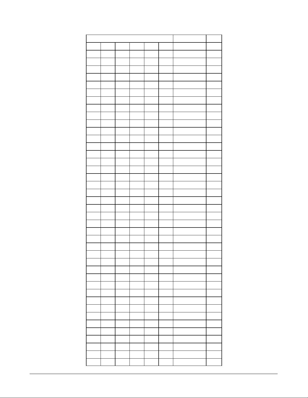
Table 2. AMD Processor 6−bit VID Code
(VID) Codes Nominal V
V
ID5VID4VID3VID2VID1VID0
0 0 0 0 0 0 1.550 V
0 0 0 0 0 1 1.525 V
0 0 0 0 1 0 1.500 V
0 0 0 0 1 1 1.475 V
0 0 0 1 0 0 1.450 V
0 0 0 1 0 1 1.425 V
0 0 0 1 1 0 1.400 V
0 0 0 1 1 1 1.375 V
0 0 1 0 0 0 1.350 V
0 0 1 0 0 1 1.325 V
0 0 1 0 1 0 1.300 V
0 0 1 0 1 1 1.275 V
0 0 1 1 0 0 1.250 V
0 0 1 1 0 1 1.225 V
0 0 1 1 1 0 1.200 V
0 0 1 1 1 1 1.175 V
0 1 0 0 0 0 1.150 V
0 1 0 0 0 1 1.125 V
0 1 0 0 1 0 1.100 V
0 1 0 0 1 1 1.075 V
0 1 0 1 0 0 1.050 V
0 1 0 1 0 1 1.025 V
0 1 0 1 1 0 1.000 V
0 1 0 1 1 1 0.975 V
0 1 1 0 0 0 0.950 V
0 1 1 0 0 1 0.925 V
0 1 1 0 1 0 0.900 V
0 1 1 0 1 1 0.875 V
0 1 1 1 0 0 0.850 V
0 1 1 1 0 1 0.825 V
0 1 1 1 1 0 0.800 V
0 1 1 1 1 1 0.775 V
1 0 0 0 0 0 0.7625 V
1 0 0 0 0 1 0.7500 V
1 0 0 0 1 0 0.7375 V
1 0 0 0 1 1 0.7250 V
1 0 0 1 0 0 0.7125 V
1 0 0 1 0 1 0.7000 V
1 0 0 1 1 0 0.6875 V
1 0 0 1 1 1 0.6750 V
1 0 1 0 0 0 0.6625 V
out
Units
http://onsemi.com
18
Page 19
NCP5392
www.BDTIC.com/ON
Table 2. AMD Processor 6−bit VID Code
(VID) Codes UnitsNominal V
V
V
ID5
ID4
1 0 1 0 0 1 0.6500 V
1 0 1 0 1 0 0.6375 V
1 0 1 0 1 1 0.6250 V
1 0 1 1 0 0 0.6125 V
1 0 1 1 0 1 0.6000 V
1 0 1 1 1 0 0.5875 V
1 0 1 1 1 1 0.5750 V
1 1 0 0 0 0 0.5625 V
1 1 0 0 0 1 0.5500 V
1 1 0 0 1 0 0.5375 V
1 1 0 0 1 1 0.5250 V
1 1 0 1 0 0 0.5125 V
1 1 0 1 0 1 0.5000 V
1 1 0 1 1 0 0.4875 V
1 1 0 1 1 1 0.4750 V
1 1 1 0 0 0 0.4625 V
1 1 1 0 0 1 0.4500 V
1 1 1 0 1 0 0.4375 V
1 1 1 0 1 1 0.4250 V
1 1 1 1 0 0 0.4125 V
1 1 1 1 0 1 0.4000 V
1 1 1 1 1 0 0.3875 V
1 1 1 1 1 1 0.3750 V
V
V
ID3
ID2
V
V
ID1
ID0
out
http://onsemi.com
19
Page 20

NCP5392
www.BDTIC.com/ON
FUNCTIONAL DESCRIPTION
General
The NCP5392 provides up to four−phase buck solution
which combines differential voltage sensing, differential
phase current sensing, and adaptive voltage positioning to
provide accurately regulated power necessary for both
Intel VR11.1 and AMD CPU power system. NCP5392 has
been designed to work with the NCP5359 driver.
Remote Output Sensing Amplifier(RSA)
A true differential amplifier allows the NCP5392 to
measure V
ground reference point by connecting the V
point to VSP, and the V
This configuration keeps ground potential differences
between the local controller ground and the V
reference point from affecting regulation of V
V
and V
core
subtracts the DAC (minus VID offset) voltage, thereby
producing an unamplified output error voltage at the
DIFFOUT pin. This output also has a 1.3 V bias voltage as
the floating ground to allow both positive and negative
error voltages.
Precision Programmable DAC
A precision programmable DAC is provided and system
trimmed. This DAC has 0.5% accuracy over the entire
operating temperature range of the part. The DAC can be
programmed to support either Intel VR11 or AMD 6−bit
VID code specifications.
High Performance Voltage Error Amplifier
The error amplifier is designed to provide high slew rate
and bandwidth. Although not required when operating as
the controller of a voltage regulator, a capacitor from
COMP to VFB is required for stable unity gain test
configurations.
Gate Driver Outputs and 2/3/4 Phase Operation
The part can be configured to run in 2−, 3−, or 4−phase
mode. In 2−phase mode, phases 1 and 3 should be used to
drive the external gate drivers as shown in the 2−phase
Applications Schematic, G2 and G4 must be grounded. In
3−phase mode, gate output G4 must be grounded as shown
in the 3−phase Applications Schematic. In 4−phase mode
all 4 gate outputs are used as shown in the 4−phase
Applications Schematic. The Current Sense inputs of
unused channels should be connected to VCCP shown in
the Application Schematics. Please refer to table “PIN
CONNECTIONS vs. PHASE COUNTS” for details.
voltage feedback with respect to the V
core
core
ground reference point to VSN.
core
ground reference points. The RSA also
core
reference
ground
core
between
core
core
Differential Current Sense Amplifiers and Summing
Amplifier
Four differential amplifiers are provided to sense the
output current of each phase. The inputs of each current
sense amplifier must be connected across the current
sensing element of the phase controlled by the
corresponding gate output (G1, G2, G3, or G4). If a phase
is unused, the differential inputs to that phase’s current
sense amplifier must be shorted together and connected to
the output as shown in the 2− and 3−phase Application
Schematics.
The current signals sensed from inductor DCR are fed into
a summing amplifier to have a summed−up output (CSSUM).
Signal of CSSUM combines information of total current of all
phases in operation.
The outputs of current sense amplifiers control three
functions. First, the summing current signal (CCSUM) of
all phases will go through DROOP amplifier and join the
voltage feedback loop for output voltage positioning.
Second, the output signal from DROOP amplifier also goes
to ILIM amplifier to monitor the output current limit.
Finally, the individual phase current contributes to the
current balance of all phases by offsetting their ramp
signals of PWM comparators.
Thermal Compensation Amplifier with VDRP and VDFB
Pins
Thermal compensation amplifier is an internal amplifier
in the path of droop current feedback for additional
adjustment of the gain of summing current and temperature
compensation. The way thermal compensation is
implemented separately ensures minimum interference to
the voltage loop compensation network.
Oscillator and Triangle Wave Generator
A programmable precision oscillator is provided. The
oscillator ’s frequency is programmed by the resistance
connected from the ROSC pin to ground. The user will
usually form this resistance from two resistors in order to
create a voltage divider that uses the ROSC output voltage
as the reference for creating the current limit setpoint
voltage. The oscillator frequency range is 100 kHz per
phase to 1.0 MHz per phase. The oscillator generates up to
4 symmetrical triangle waveforms with amplitude between
1.3 V and 2.3 V. The triangle waves have a phase delay
between them such that for 2−, 3− and 4−phase operation
the PWM outputs are separated by 180, 120, and 90 angular
degrees, respectively.
http://onsemi.com
20
Page 21
NCP5392
www.BDTIC.com/ON
PWM Comparators with Hysteresis
Four PWM comparators receive an error signal at their
noninverting input. Each comparator receives one of the
triangle waves at its inverting output. The output of each
comparator generates the PWM outputs G1, G2, G3, and
G4.
During steady state operation, the duty cycle will center
on the valley of the triangle waveform, with steady state
duty cycle calculated by V
both high and low comparator output transitions shift phase
to the points where the error signal intersects the down and
up ramp of the triangle wave.
PROTECTION FEATURES
Undervoltage Lockout (VCC and 12VMON)
An undervoltage lockout (UVLO) senses the VCC input
directly. 12 V UVLO senses the 12 V power supply by
connecting it to the 12VMON pin through an appropriate
resistor divider. During power−up, both the VCC input and
12VMON are monitored, and the PWM outputs and the
soft−start circuit are disabled until both input voltages
exceed the threshold voltages of their individual UVLO
comparators. The UVLO comparators both incorporate
hysteresis to avoid chattering.
Overcurrent Shutdown
A programmable overcurrent function is incorporated
within the IC. A comparator and latch make up this
function. The inverting input of the comparator is
connected to the ILIM pin. The voltage at this pin sets the
maximum output current the converter can produce. The
ROSC pin provides a convenient and accurate reference
voltage from which a resistor divider can create the
overcurrent setpoint voltage. Although not actually
disabled, tying the ILIM pin directly to the ROSC pin sets
the limit above useful levels − effectively disabling
overcurrent shutdown. The comparator noninverting input
is the summed current information from the VDRP minus
offset voltage. The overcurrent latch is set when the current
information exceeds the voltage at the ILIM pin. The
outputs are pulled low, and the soft−start is pulled low. The
outputs will remain disabled until the VCC voltage is
removed and re−applied, or the ENABLE input is brought
low and then high.
. During a transient event,
out/Vin
Soft−Start
There are two possible soft−start modes: AMD and
VR11. AMD mode simply ramps V
to the DAC setting at a fixed rate. The VR11 mode ramps
V
to 1.1 V boot voltage at a fixed rate of 0.8 mV/S,
core
pauses at 1.1 V for around 500 S, reads the VID pins to
determine the DAC setting. Then ramps V
DAC setting at the Dynamic VID slew rate of up to
12.5 mV/S. Typical AMD and VR11 soft−start sequences
are shown in the following graphs (Figure 9 and 10).
APPLICATION INFORMATION
The NCP5392 demo board for the NCP5392 is available
by request. It is configured as a four phase solution with
decoupling designed to provide a 1 m load line under a
100 A step load.
Startup Procedure
Start by installing the test tool software. It is best to
power the test tool from a separate ATX power supply. The
test tool should be set to a valid VID code of 0.5 V or above
in order for the controller to start. Consult the VTT help
manual for more detailed instruction.
Step Load Testing
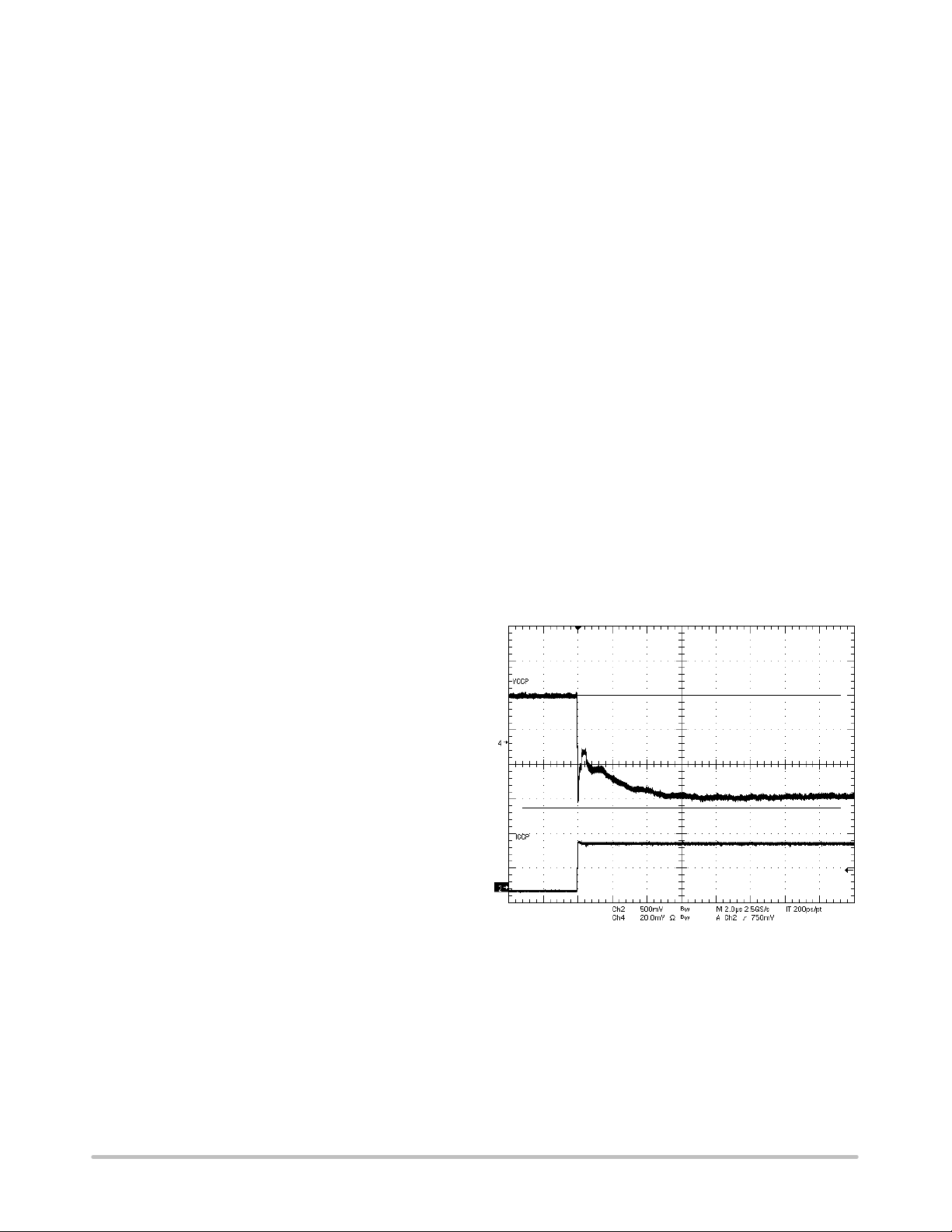
The VTT tool is used to generate the di/dt step load.
Select the dynamic loading option in the VTT test tool
software. Set the desired step load size, frequency, duty,
and slew rate. See Figure 6.
from 0 V directly
core
to the final
core
Output Overvoltage and Undervoltage Protection and
Power Good Monitor
An output voltage monitor is incorporated. During
normal operation, if the output voltage is 180 mV (typical)
over the DAC voltage, the VR_RDY goes low, the DRVON
signal remains high, the PWM outputs are set low. The
outputs will remain disabled until the VCC voltage is
removed and reapplied. During normal operation, if the
output voltage falls more than 350 mV below the DAC
setting, the VR_RDY pin will be set low until the output
voltage rises.
http://onsemi.com
Dynamic VID Testing
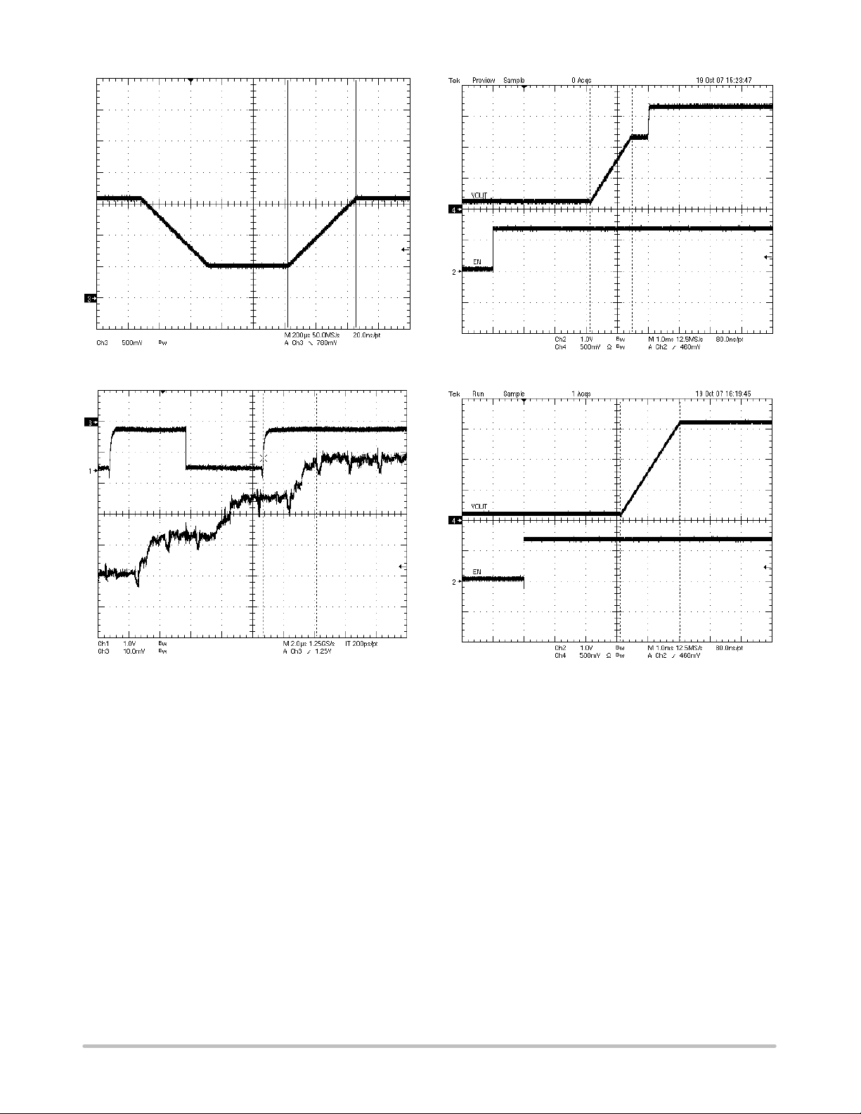
Intel Requirements. Select the Dynamic VID option.
Before enabling the test set the lowest VID to 0.5 V or
greater and set the highest VID to a value that is greater than
the lowest VID selection, then enable the test. See Figures
7 and 8.
21
Figure 6. Typical Load Step Response
(full load, 35 A − 100 A)
The VTT tool provides for VID stepping based on the
Page 22
NCP5392
www.BDTIC.com/ON
Figure 7. 1.6 V to 0.5 V Dynamic VID response
Figure 8. Dynamic VID Settling Time Rising
(CH1: VID1, CH2: DAC, CH3:VCCP)
Design Methodology
Decoupling the VCC Pin on the IC
An RC input filter is required as shown in the VCC pin to
minimize supply noise on the IC. The resistor should be
sized such that it does not generate a large voltage drop
between 5 V supply and the IC.
Understanding Soft−Start
The controller supports two different startup routines. An
AMD ramp to the initial VID code, or a VR11 Ramp to the
1.1 V boot voltage, with a pause to capture the VID code
then resume ramping to target value based on internal slew
rate limit. The initial ramp rate was set to be 0.8 mV/S.
Figure 9. VR11.1 Startup
Figure 10. AMD Startup
Programming the Current Limit and the Oscillator
Frequency
The demo board is set for an operating frequency of
approximately 330 kHz. The R
reference voltage which is divided down with a resistor
divider and fed into the current limit pin ILIM. Then
calculate the individual RLIM1 and RLIM2 values for the
divider. The series resistors RLIM1 and RLIM2 sink
current from the ILIM pin to ground. This current is
internally mirrored into a capacitor to create an oscillator.
The period is proportional to the resistance and frequency
is inversely proportional to the total resistance. The total
resistance may be estimated by Equation 1. This equation
is valid for the individual phase frequency in both three and
four phase mode.
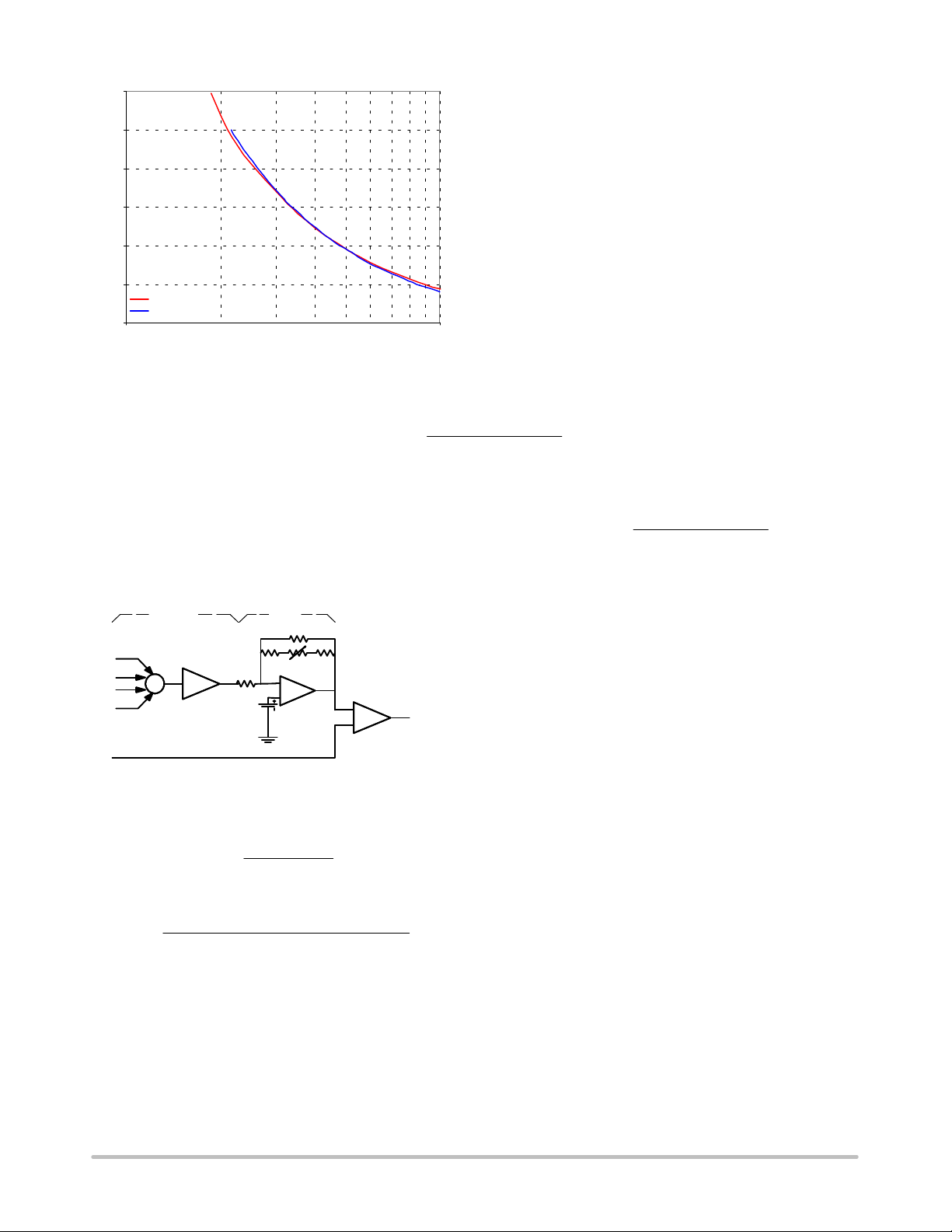
R
^ 20947 F
osc
30.5 k ^ 20947 330
pin provides a 2.0 V
OSC
*1.1262
SW
*1.1262
(eq. 1)
http://onsemi.com
22
Page 23
NCP5392
www.BDTIC.com/ON
60
current of all phases multiplied by a controlled gain
50
(Acssum*Adrp). DCR sensed inductor current is a function
of the winding temperature. The best approach is to set the
40
maximum current limit based on expected average
maximum temperature of the inductor windings,
30
Rosc−kohm
20
10
Calculation
Real
0
100 1000
Freq−kHz
Figure 11. ROSC vs. Frequency
For multiphase controller, the ripple current can be calculated as,
(Vin* N @ V
Ipp +
L @FSW@ V
Therefore calculate the current limit voltage as below,
V
V
LIMIT
LIMIT
^ A
^ A
CSSUM
CSSUM
@ A
@ A
DRP
DRP
@ DCR
@ DCR
Tmax
Tmax
@ (I
@ǒI
The current limit function is based on the total sensed
DCR
) @ V
out
in
MIN_OCP
MIN_OCP
+ DCR
Tmax
out
@)0.5 @ Ipp)
@)0.5 @
(1 ) 0.00393 @ (T
25C
* N @ V
(V
in
L @FSW@ V
out
) @ V
in
max
* 25))
out
Ǔ
(eq. 2)
(eq. 3)
(eq. 4)
In Equation 4, A
Acssum Adrp
I1
I2
I3
I4
+
Ilim
CSSUM
RISO1
RSUM
and A
RNOR
−
+
DRP
RT2
Figure 12. ACSSUM and ADRP
As introduced before, V
comes from a resistor
LIMIT
divider connected to Rosc pin, thus,
R
R
LIM1
ISO1
) R
LIM2
) R
) R
ISO2
A
DRP
V
A
+*
LIMIT
CSSUM
(R
NOR
+ 2V@
+*4
R
NOR
) R
@ (R
ISO1
are the gain of current summing amplifier and droop amplifier.
R
ISO1
and R
are in series with RT2, the NTC
ISO2
temperature sense resistor placed near inductor. R
RISO2
the resistor connecting between pin VDFB and pin
CSSUM. If PSI = 1, PSI function is off, the current limit
follows the Equation 7; if PSI = 0, the power saving mode
+
−
OCP
event
will be enabled, COEpsi is a coefficient for the current
limiting related with power saving function (PSI), the
current limit can be calculated from Equation 8. COEpsi
value is one over the original phase count N. Refer to the
PSI and phase shedding section for more details.
@ COEpsi
LIM2
) RT2)
ISO2
) RT2) @ R
(eq. 5)
(eq. 6)
SUM
SUM
is
http://onsemi.com
23
Page 24

NCP5392
www.BDTIC.com/ON
Final Equations for the Current Limit Threshold
Final equations are described based on two conditions: normal mode and PSI mode.
2V@R
LIM2
R
@ DCR
SUM
LIM2
@ DCR
LIM1)RLIM2
(1 ) 0.00393 @ (T
25C
@ COEpsi
(1 ) 0.00393 @ (T
25C
inductor
inductor
* 25))
I
LIMIT
I
LIMIT
(normal) ^
(PSI) ^
4 @
R
@(R
4 @
NOR
(R
NOR)RISO1)RISO2
R
@(R
NOR
(R
NOR)RISO1)RISO2
ISO1)RISO2
ISO1)RISO2
)RT2)@R
)RT2)
)RT2)@R
)RT2)
2V@R
R
LIM1)RLIM2
SUM
* 25))
* 0.5 @
* 0.5 @
(Vin* V
(Vin* N @ V
L @ FSW@ V
) @ V
out
L @ FSW@ V
) @ V
out
out
in
(eq. 7)
out
in
(eq. 8)
N is the number of phases involved in the circuit.
The inductors on the demo board have a DCR at 25°C of
0.6 m. Selecting the closest available values of 21.3 k
for R
operating frequency of 330 kHz. Select R
= 1 k, RT2 = 10 K (25°C), R
and 9.28 k for R
LIM1
yields a nominal
LIM2
ISO
NOR/RSUM
= 2, (refer to
1 = 1 k, R
ISO2
application diagram). That results to an approximate
current limit of 133 A at 100°C for a four phase operation
and 131 A at 25°C. The total sensed current can be
observed as a scaled voltage at the VDRP with a positive
no−load offset of approximately 1.3 V.
Inductor Selection
When using inductor current sensing it is recommended
that the inductor does not saturate by more than 10% at
maximum load. The inductor also must not go into hard
saturation before current limit trips. The demo board
includes a four phase output filter using the T44−8 core
from Micrometals with 3 turns and a DCR target of 0.6 m
@ 25°C. Smaller DCR values can be used, however,
current sharing accuracy and droop accuracy decrease as
DCR decreases. Use the NCP5392 design aide for
regulation accuracy calculations for specific value of DCR.
Inductor Current Sensing Compensation
The NCP5392 uses the inductor current sensing method.
An RC filter is selected to cancel out the impedance from
inductor and recover the current information through the
inductor’s DCR. This is done by matching the RC time
constant of the sensing filter to the L/DCR time constant.
The first cut approach is to use a 0.1 F capacitor for C and
then solve for R.
(eq. 9)
R
sense
(T) +
0.1 @ F @DCR
L
@ (1 ) 0.00393(T * 25))
25C
Because the inductor value is a function of load and
inductor temperature final selection of R is best done
experimentally on the bench by monitoring the V
droop
pin
and performing a step load test on the actual solution.
http://onsemi.com
24
Page 25
NCP5392
www.BDTIC.com/ON
Simple Average SPICE Model
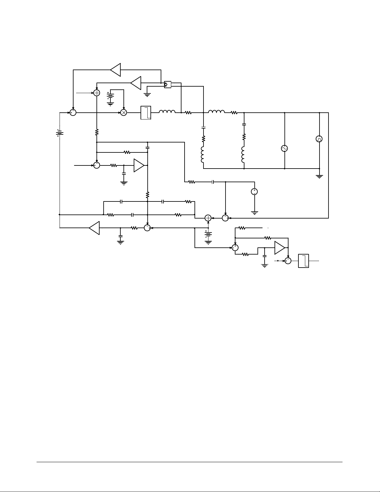
A simple state average model shown in Figure 13 can be used to determine a stable solution and provide insight into the
control system.
GAIN = 1
VRamp_min
1.3V
Unity Gain BW=15MHz
Voff
Voff
1E3
RSUM
1k
RF
2.2k
0
R8
1k
V3
12V
CH
22p
{−2/3*4}
RDFB
2k
C5
10.6p
0
R6
C4
10.6p
0
22p
R12
5.11k
CF
1.8n
1k
0
12
1E3
+
−
GAIN = {6}
0
1
{185e−9/4}
CDFB
Vdrp
CFB1
680P
E1
L
+
−
E
2
{0.6E−3/4}
RFB1
69.8
RFB
1k
Voff
DCR
RDAC
50
Figure 13. NCP5392 Average SPICE Model
LBRD
1 2
100p
CBulk
{560e−6*6}
ESRBulk
{7e−3/6}
2
ESLBulk
{3.5e−9/6}
1
CDAC
12n
Voffset
1.3V
0
RBRD
0.75m
CCer
2
{1.5e−9/18}
1
DC = 1.2V
AC = 0
R11
1k
R9
1kC610.6p
{22e−6*18}
ESRCer
{1.5e−3/18}
0Aac
ESLCer
0Adc
VDAC
TRAN = PULSE
(0 0.05 400u 5u 5u 500u 1000u)
0
Vdrp
R10
1E3
2k
Voff
0
I2 = 110
TD = 100u
TR = 50n
TF = 50n
PW = 100u
PER = 200u
I1 = 50
IMON
I1
Vout
0
Compensation and Output Filter Design
If the required output filter and switching frequency are
significantly different, it’s best to use the available PSPICE
models to design the compensation and output filter from
scratch.
The design target for this demo board was 1.0 m up to
2.0 MHz. The phase switching frequency is currently set to
330 kHz. It can easily be seen that the board impedance of
0.75 m between the load and the bulk capacitance has a
large effect on the output filter. In this case the six 560 F
bulk capacitors have an ESR of 7.0 m. Thus the bulk ESR
plus the board impedance is 1.15 m + 0.75 m or
1.9 m. The actual output filter impedance does not drop
to 1.0 m until the ceramic breaks in at over 375 kHz. The
controller must provide some loop gain slightly less than
one out to a frequency in excess 300 kHz. At frequencies
below where the bulk capacitance ESR breaks with the
bulk capacitance, the DC−DC converter must have
sufficiently high gain to control the output impedance
completely. Standard Type−3 compensation works well
with the NCP5392.
http://onsemi.com
25
Page 26
dB
www.BDTIC.com/ON
NCP5392
Zout Open Loop
Zout Closed Loop
Open Loop Gain with Current Loop Closed
Voltage Loop Compensation Gain
80
60
40
20
0
−20
−40
−60
−80
−100
100 1000 10000 100000 1000000 10000000
1mOhm
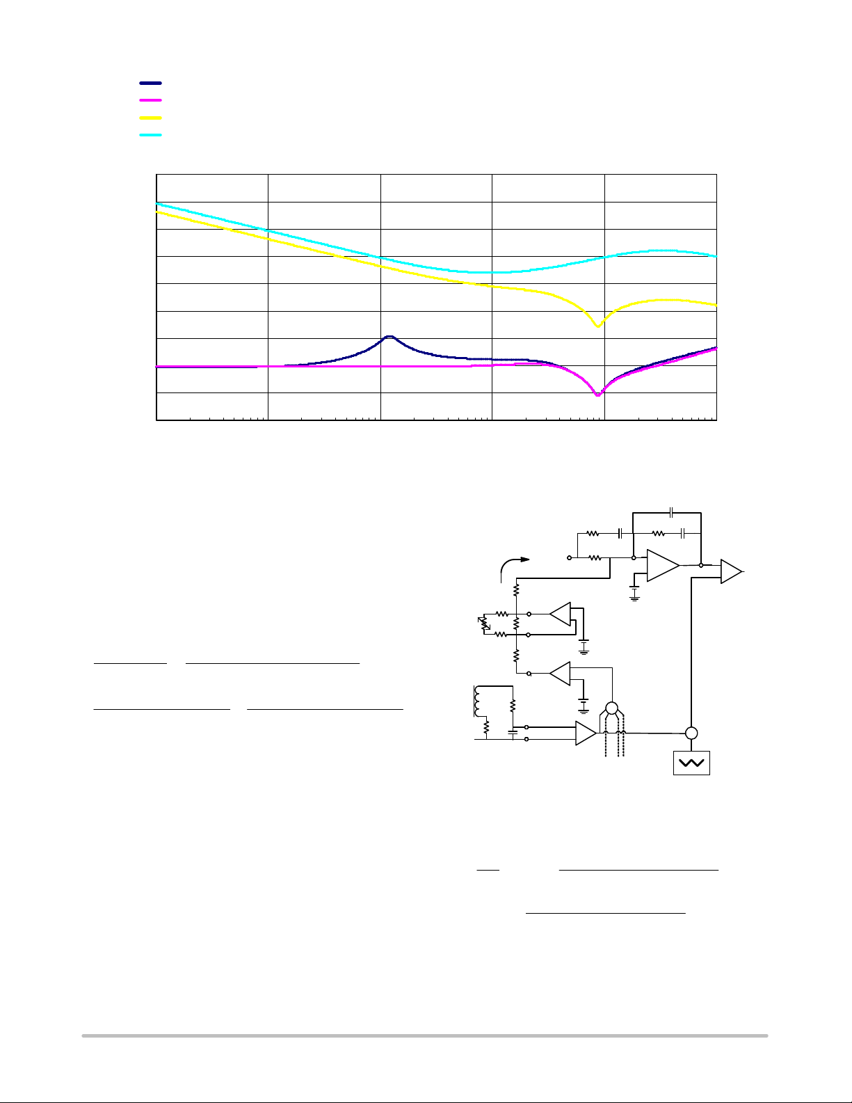
Figure 14. NCP5392 Circuit Frequency Response
The goal is to compensate the system such that the
resulting gain generates constant output impedance from
DC up to the frequency where the ceramic takes over
holding the impedance below 1.0 m. See the example of
the locations of the poles and zeros that were set to optimize
the model above.
By matching the following equations a good set of
starting compensation values can be found for a typical
mixed bulk and ceramic capacitor type output filter.
1
2 @ CF @ RF
2 @ CFB1 @ (RFB1 ) RFB)
+
2 @ (RBRD ) ESR
1
+
2 @ C
1
Bulk
@ (RBRD )ESR
Cer
) @ C
1
(eq. 10)
Bulk
(eq. 11)
Bulk
RFB should be set to provide optimal thermal
compensation in conjunction with thermistor RT2, R
and R
. With RFB set to 1.0 k, R
ISO2
is usually set to
FB1
ISO1
100 for maximum phase boost, and the value of RF is
typically set to 3.0 k.
Droop Injection and Thermal Compensation
The VDRP signal is generated by summing the sensed
output currents for each phase. A droop amplifier is added
to adjust the total gain to approximately eight. VDRP is
externally summed into the feedback network by the
resistor RDRP. This introduces an offset which is
proportional to the output current thereby forcing a
controlled, resistive output impedance.
Frequency
)
CH
RT
RL
I Bias
RDRP
RISO2
RISO1
RSUM
RSx
CSx
Droop
Amp
RNOR
Gain = 4
CSSUM
Amp
RFB1
+
−
−
+
1.3 V
+
−
Gain = 1
CFB1
RFB
1.3 V
1.3 V
+
RF
−
+
Error
Amp
CF
+
−
PWM
Comparator
+
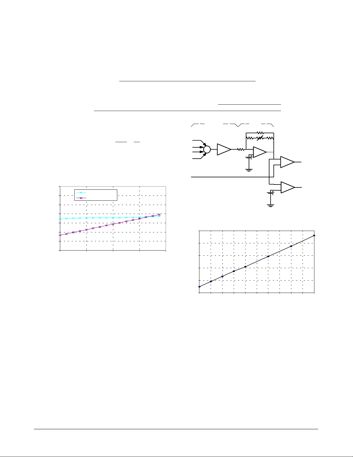
Figure 15. Droop Injection and Thermal
Compensation
RDRP determines the target output impedance by the
basic equation:
V
R
I
out
out
DRP
+ Z
+
out
R
+
FB
@ DCR @ A
FB
@ DCR @ A
Z
CSSUM
out
R
DRP
CSSUM
@ A
DRP
@ A
DRP
(eq. 12)
(eq. 13)
R
The value of the inductor’s DCR is a function of
temperature according to the Equation 14:
DCR (T) + DCR
@ (1 ) 0.00393 @ (T * 25))
25C
(eq. 14)
http://onsemi.com
26
Page 27
NCP5392
www.BDTIC.com/ON
Actual DCR increases by temperature, the system can be
thermally compensated to cancel this effect to a great
degree by adding an NTC in parallel with R
NOR
to reduce
the droop gain as the temperature increases. The NTC
device is nonlinear. Putting a resistor in series with the NTC
helps make the device appear more linear with
R
@ DCR
Z
(T) +
out
FB
@ (1 ) 0.00393 @ (T *25)) @ A
25C
temperature. The series resistor is split and inserted on both
sides of the NTC to reduce noise injection into the feedback
loop. The recommended total value for R
approximately 1.0 k.
The output impedance varies with inductor temperature
by the equation:
R
DRP
CSSUM
By including the NTC RT2 and the series isolation resistors the new equation becomes:
R
RFB@ DCR
Z
(T) +
out
@ (1 ) 0.00393 @ (T *25)) @ A
25C
The typical equation of an NTC is based on a curve fit
R
CSSUM
DRP
Acssum Adrp
NOR
@
(R
NOR)RISO1)RISO2
Equation 17
1
RT2(T) + RT2
25C
@ e
ƪǒ
273)T
Ǔ*ǒ
298
1
Ǔƫ
(eq. 17)
The demo board use a 10 k NTC with a value of 3740.
Figure 16 shows the comparison of the compensated output
impedance and uncompensated output impedance varying
with temperature.
0.0013
0.0012
0.0011
Ohm
0.0009
0.0008
0.0007
0.0006
0.001
25 45 65 85 105
Figure 16. Z
Zout
Zout(uncomp)
Celsius
vs. Temperature
out
IMON for Current Monitor
Since VDRP signal reflects the current information of all
phases. It can be fed into the IMON amplifier for current
monitoring as shown in Figure 17. IMON amplifier has a
fixed gain of 2 with an offset when VDRP is equal to 1.3 V,
the internal floating reference voltage. The IMON
amplifier will be saturated at an maximum output of 1.09 V
therefore the total gain of current should be carefully
considered to make the maximum load current indicated by
the IMON output. Figure 18 shows a typical of the relation
between IMON output and the load current.
I1
I2
+
I3
I4
Ilim
1.05
0.84
0.63
0.42
Vimon−V
0.21
0
0 102030405060708090100
Figure 18. IMON Output vs. Output Current
Power Saving Indicator (PSI) and Phase Shedding
VR11.1 requires the processor to provide an output
signal to the VR controller to indicate when the processor
is in a low power state. NCP5392 use the status of PSI pin
to decide if there is a need to change its operating state to
maximize efficiency at light loads. When PSI = 0, the PSI
RISO1
RSUM
Figure 17. IMON Circuit
function will be enabled, and VR system will be running at
a single phase power saving mode.
The PSI signal will de−assert 1 s prior to moving to a
normal power state.
At power saving mode, NCP5392 works with the
NCP5359 driver to represent diode emulation mode at light
load for further power saving.
When system switches on PSI function, an phase
shedding will be presented. Only one phase is active in the
@ A
DRP
@(R
ISO1)RISO2
RNOR
Vimon vs. Iout
Iout−A
)RT2)@R
RT2
−
+
)RT2)
ISO1
SUM
RISO2
plus R
+
−
+
−
Gain = 2
ISO2
(eq. 15)
(eq. 16)
OCP
event
Imon
is
http://onsemi.com
27
Page 28
NCP5392
www.BDTIC.com/ON
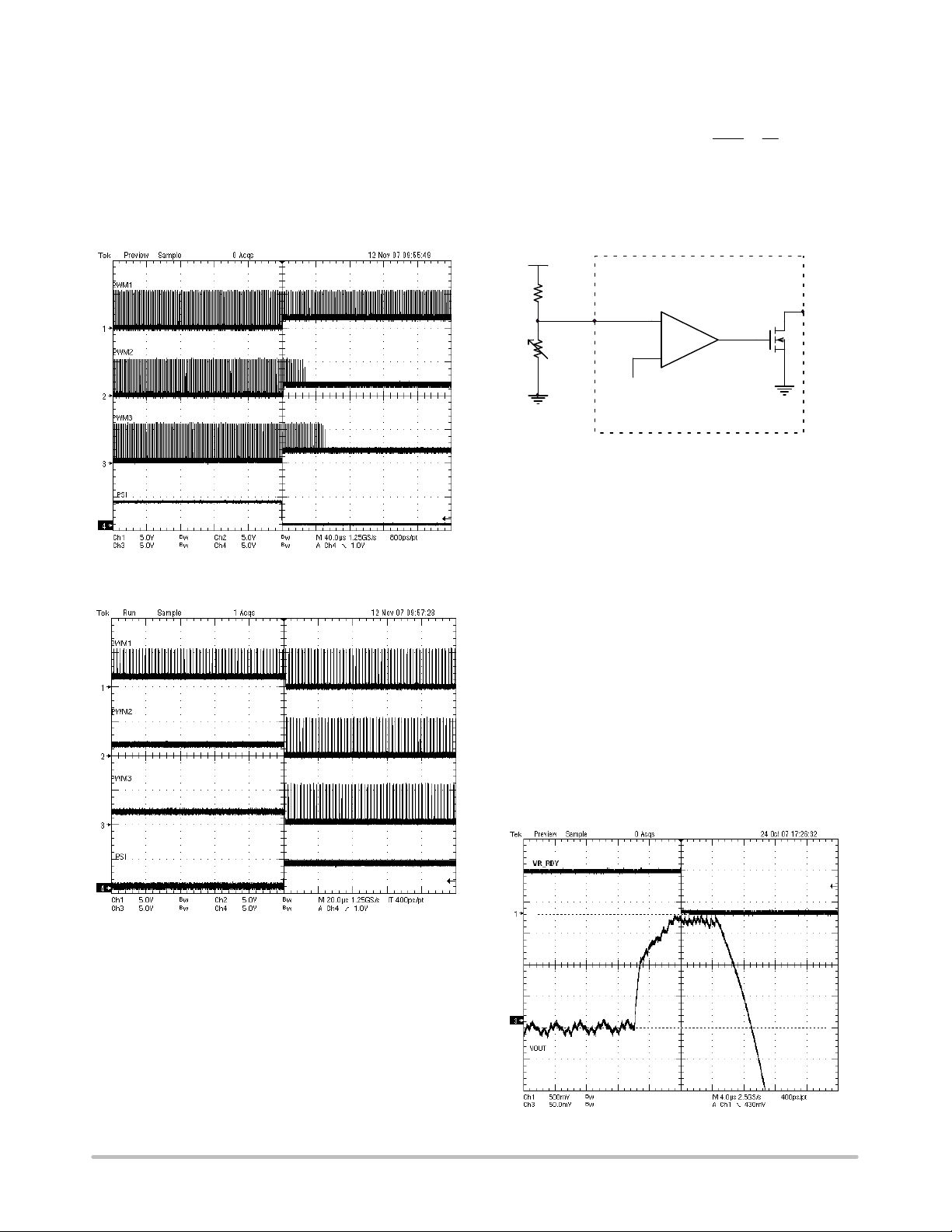
emulation mode while other phases are shed. Figure 19
indicates a PSI−on transition from a 3−phase mode to a
single phase mode. While staying stable in PSI mode, the
PWM signal of phase 1 will vary from a mid−state level
(1.5 V typical) to high level while other phases all go to
mid−state level. Vice verse, when PSI signal goes high, the
system will go back to the original phase mode such as
shown in Figure 20.
Figure 19. PSI turns on, CH1: PWM1, CH2: PWM2,
CH3: PWM3, CH4: PSI
impedance. The following equations can be used to find the
temperature trip points.
1
RT1(T) + RT1
25C
@ e
ƪǒ
273)T
Ǔ*ǒ
298
1
Ǔƫ
(eq. 18)
With a beta value of 3740, a 68 k NTC resistor is
selected for RT1, RNTC1 is populated with 19.6 k.
VR_HOT threshold is carefully selected to make sure when
board temperature is less than 92°C.
VCC
RNTC1
NTC
RT1
0.268 Vcc
0
Figure 21. VRHOT Circuit
OVP Improved Performance
+
−
OUT
VRHOT
0
The overvoltage protection threshold is not adjustable.
OVP protection is enabled as soon as soft−start begins and
is disabled when part is disabled. When OVP is tripped, the
controller commands all four gate drivers to enable their
low side MOSFETs and VR_RDY transitions low. In order
to recover from an OVP condition, VCC must fall below the
UVLO threshold. See the state diagram for further details.
The OVP circuit monitors the output of DIFFOUT. If the
DIFFOUT signal reaches 180 mV (typical) above the
nominal 1.3 V offset the OVP will trip and VRRDY will be
pulled low, after eight consecutive OVP events are
detected, all PWMs will be latched. The DIFFOUT signal
is the difference between the output voltage and the DAC
voltage (minus 19 mV if in VR11.1 modes) plus the 1.3 V
internal offset. This results in the OVP tracking on the DAC
voltage even during a dynamic change in the VID setting
during operation.
Figure 20. PSI turns off, CH1: PWM1, CH2: PWM2,
CH3: PWM3, CH4: PSI
VRHOT
Thermal monitoring circuit consists of one sensitive
comparator that compares the voltage on the NTC pin with
an internal voltage reference. VR_HOT is an open drain
type of output. In normal temperature, the voltage value on
NTC pin is higher than the internal reference, VR_HOT
will be low impedance. When the temperature is higher
than certain threshold, the VR_HOT will be high
Figure 22. VR11.1, 1.6 V OVP Event
http://onsemi.com
28
Page 29
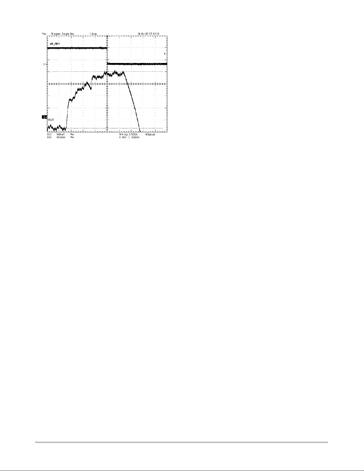
Figure 23. AMD, 1.55 V OVP Event
www.BDTIC.com/ON
NCP5392
Gate Driver and MOSFET Selection
ON Semiconductor provides the NCP5359 as a
companion gate driver IC. The NCP5359 driver is
optimized to work with a range of MOSFETs commonly
used in CPU applications. The NCP5359 provides special
functionality including power saving mode operation and
is required for high performance dynamic VID operation.
Contact your local ON Semiconductor applications
engineer for MOSFET recommendations.
Board Stackup and Board Layout
Close attention should be paid to the routing of the sense
traces and control lines that propagate away from the
controller IC. Routing should follow the demo board
example. For further information or layout review contact
ON Semiconductor.
http://onsemi.com
29
Page 30
EN
www.BDTIC.com/ON
VID
NCP5392
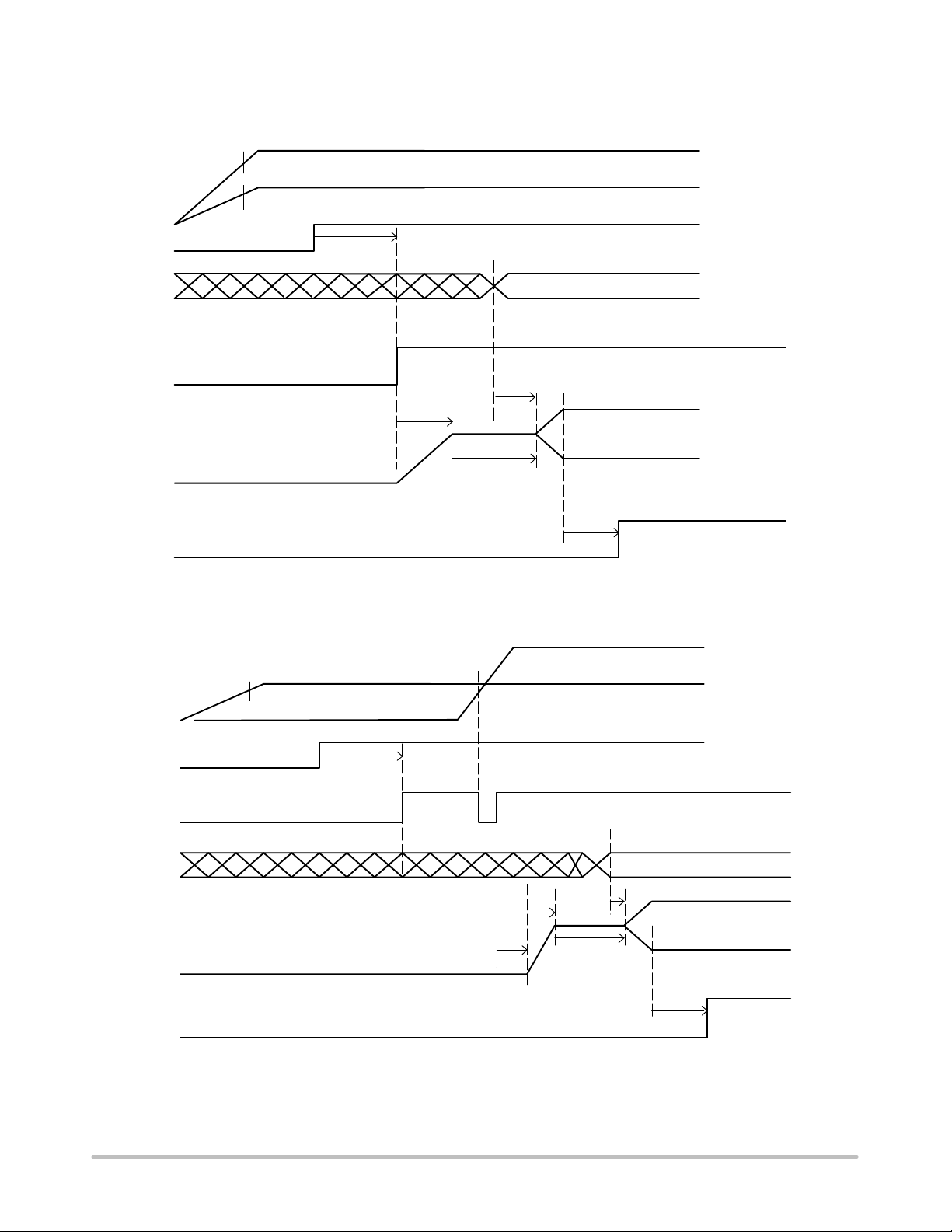
SYSTEM TIMING DIAGRAM
12 V (Gate Driver)
UVLO
5 V (Controller)
UVLO
3.5 ms
Valid VID
DRVON
VSP−VSN
VR_RDY
UVLO
EN
DRVON
1 s min
1.5 ms
500 s
500 s
Figure 24. Normal Startup
12 V (Gate Driver)
UVLO
5 V (Controller)
POR
3.5 ms
VID
1.5 ms
VSP−VSN
VR_RDY
1 ms
Figure 25. Driver UVLO Limited Startup
http://onsemi.com
30
500 s
Valid VID
1 s min
500 s
Page 31
NCP5392
www.BDTIC.com/ON
12345678
Diffout ~ 1.3 V
VR_RDY
DRVON = High
VSP = VID − 19 mV
185 mV
12345678
185 mV
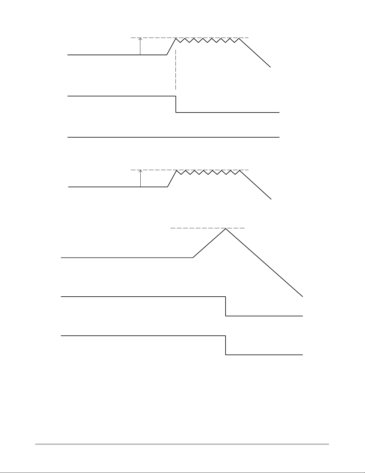
Figure 26. OVP Shutdown
VDRP
VR_RDY
DRVON
I
+ 1.3
limit
Figure 27. Non−PSI Current Limit
http://onsemi.com
31
Page 32
PIN ONE
a
www.BDTIC.com/ON
LOCATION
2X
2X
40X
EXPOSED PAD
0.05 C
0.15 C
0.15 C
0.10 C
0.08 C
L
40X
b
40X
A0.10 BC
TOP VIEW
SIDE VIEW
11
10
1
40
BOTTOM VIEW
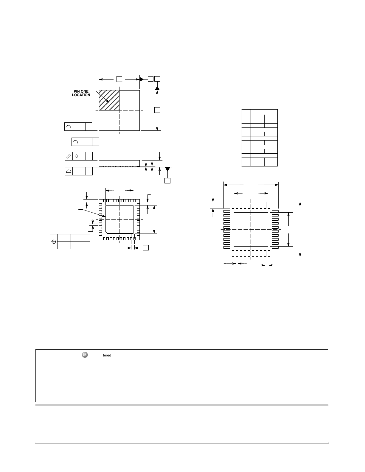
PACKAGE DIMENSIONS
D A B
(A3)
A1
D2
20
K
40X
21
E2
30
31
36X
e
NCP5392
QFN40 6x6, 0.5P
CASE 488AR−01
ISSUE A
E
A
SEATING
C
PLANE
NOTES:
1. DIMENSIONING AND TOLERANCING PER
ASME Y14.5M, 1994.
2. CONTROLLING DIMENSIONS: MILLIMETERS.
3. DIMENSION b APPLIES TO PLATED
TERMINAL AND IS MEASURED BETWEEN
0.25 AND 0.30mm FROM TERMINAL
4. COPLANARITY APPLIES TO THE EXPOSED
PAD AS WELL AS THE TERMINALS.
MILLIMETERS
DIM MIN MAX
A 0.80 1.00
A1 0.00 0.05
A3 0.20 REF
b 0.18 0.30
D 6.00 BSC
D2 4.00 4.20
E 6.00 BSC
e 0.50 BSC
L 0.30 0.50
K 0.20 −−−
4.20E2 4.00
SOLDERING FOOTPRINT*
6.30
4.20
40X
0.65
1
4.20
6.30
40X
0.30
DIMENSIONS: MILLIMETERS
*For additional information on our Pb−Free strategy and soldering
details, please download the ON Semiconductor Soldering and
Mounting Techniques Reference Manual, SOLDERRM/D.
36X
0.50 PITCH
ON Semiconductor and are registered trademarks of Semiconductor Components Industries, LLC (SCILLC). SCILLC reserves the right to make changes without further notice
to any products herein. SCILLC makes no warranty, representation or guarantee regarding the suitability of its products for any particular purpose, nor does SCILLC assume any
liability arising out of the application or use of any product or circuit, and specifically disclaims any and all liability, including without limitation special, consequential or incidental
damages. “Typical” parameters which may be provided in SCILLC data sheets and/or specifications can and do vary in different applications and actual performance may vary over
time. All operating parameters, including “Typicals” must be validated for each customer application by customer’s technical experts. SCILLC does not convey any license under
its patent rights nor the rights of others. SCILLC products are not designed, intended, or authorized for use as components in systems intended for surgical implant into the body,
or other applications intended to support or sustain life, or for any other application in which the failure of the SCILLC product could create a situation where personal injury or death
may occur. Should Buyer purchase or use SCILLC products for any such unintended or unauthorized application, Buyer shall indemnify and hold SCILLC and its officers, employees,
subsidiaries, affiliates, and distributors harmless against all claims, costs, damages, and expenses, and reasonable attorney fees arising out of, directly or indirectly, any claim of
personal injury or death associated with such unintended or unauthorized use, even if such claim alleges that SCILLC was negligent regarding the design or manufacture of the part.
SCILLC is an Equal Opportunity/Affirmative Action Employer. This literature is subject to all applicable copyright laws and is not for resale in any manner.
PUBLICATION ORDERING INFORMATION
LITERATURE FULFILLMENT:
Literature Distribution Center for ON Semiconductor
P.O. Box 5163, Denver, Colorado 80217 USA
Phone: 303−675−2175 or 800−344−3860 Toll Free USA/Canada
Fax: 303−675−2176 or 800−344−3867 Toll Free USA/Canada
Email: [email protected]
N. American Technical Support: 800−282−9855 Toll Free
USA/Canada
Europe, Middle East and Africa Technical Support:
Phone: 421 33 790 2910
Japan Customer Focus Center
Phone: 81−3−5773−3850
http://onsemi.com
32
ON Semiconductor Website: www.onsemi.com
Order Literature: http://www.onsemi.com/orderlit
For additional information, please contact your loc
Sales Representative
NCP5392/D
 Loading...