

NCP3218A Datasheet (PDF) - ON Semiconductor - 7-Bit, Programmable, 3-Phase, Mobile CPU Synchronous Buck Controller
Datasheet NCP3218A Datasheet (PDF) - ON Semiconductor - 7-Bit, Programmable, 3-Phase, Mobile CPU Synchronous Buck Controller Datasheet
Page 1

ADP3212A, NCP3218A
7-Bit, Programmable,
3-Phase, Mobile CPU
Synchronous Buck Controller
The APD3212A/NCP3218A is a highly efficient, multi−phase,
synchronous buck switching regulator controller. With its integrated
drivers, the APD3212A/NCP3218A is optimized for converting the
notebook battery voltage into the core supply voltage required by high
performance Intel processors. An internal 7−bit DAC is used to read a
VID code directly from the processor and to set the CPU core voltage
to a value within the range of 0.3 V to 1.5 V. The APD3212A/
NCP3218A is programmable for 1−, 2−, or 3−phase operation. The
output signals ensure interleaved 2− or 3−phase operation.
The APD3212A/NCP3218A uses a multimode architecture run at a
programmable switching frequency and optimized for efficiency
depending on the output current requirement. The
APD3212A/NCP3218A switches between single− and multi−phase
operation to maximize efficiency with all load conditions. The chip
includes a programmable load line slope function to adjust the output
voltage as a function of the load current so that the core voltage is
always optimally positioned for a load transient. The
APD3212A/NCP3218A also provides accurate and reliable
short−circuit protection, adjustable current limiting, and a delayed
power−good output. The IC supports On−The−Fly (OTF) output
voltage changes requested by the CPU.
The APD3212A/NCP3218A are specified over the extended
commercial temperature range of −40°C to 100°C. The ADP3212A is
available in a 48−lead QFN 7x7mm 0.5mm pitch package. The
NCP3218A is available in a 48−lead QFN 6x6mm 0.4mm pitch
package. Except for the packages, the APD3212A/NCP3218A are
identical. APD3212A/NCP3218A are Halogen−Free, Pb−Free and
RoHS compliant.
http://onsemi.com
QFN48
CASE 485AJ
148
QFN48
CASE 485AN
481
MARKING DIAGRAM
1
xxP321xA
AWLYYWWG
xxx = Specific Device Code
(ADP3212A or NCP3218A)
A = Assembly Location
WL = Wafer Lot
YY = Year
WW = Work Week
G = Pb−Free Package
Features
• Single−Chip Solution
• Fully Compatible with the Intel
Specifications
®
IMVP−6.5t
• Selectable 1−, 2−, or 3−Phase Operation with Up to
1 MHz per Phase Switching Frequency
• Phase 1 and Phase 2 Integrated MOSFET Drivers
• Input Voltage Range of 3.3 V to 22 V
• Guaranteed ±8 mV Worst−Case Differentially Sensed
Core Voltage Error Over Temperature
• Automatic Power−Saving Mode Maximizes Efficiency
with Light Load During Deeper Sleep Operation
• Active Current Balancing Between Output Phases
• Independent Current Limit and Load Line Setting
Inputs for Additional Design Flexibility
Applications
• Notebook Power Supplies for Next−Generation Intel
Processors
© Semiconductor Components Industries, LLC, 2010
June, 2010 − Rev. 0
• Built−In Power−Good Blanking Supports Voltage
Identification (VID) On−The−Fly (OTF) Transients
• 7−Bit, Digitally Programmable DAC with 0.3 V to
1.5 V Output
• Short−Circuit Protection with Programmable Latchoff
Delay
• Clock Enable Output Delays the CPU Clock Until the
Core
Voltage is Stable
• Output Power or Current Monitor Options
• 48−Lead QFN 7x7mm (ADP3212A), 48−Lead QFN
6x6mm (NCP3218A)
• These are Pb−Free Devices
• Fully RoHS Compliant
ORDERING INFORMATION
See detailed ordering and shipping information in the package
dimensions section on page 33 of this data sheet.
1 Publication Order Number:
ADP3212A/D
Page 2
ADP3212A, NCP3218A
PIN ASSIGNMENT
TRDET
COMP
FB
LLINE
SWFB1
SWFB2
SWFB3
PH0
PH1
PWRGD
CLKEN
FBRTN
PWRGD
IMON
CLKEN
FBRTN
COMP
TRDET
VARFREQ
VRTT
TTSNS
GND
TRDET
Generator
+
SS
REF
CSREF
+
SS
_
+
1.55 V
DAC + 200 mV
DAC − 300 mV
PWRGD
Open
Drain
CLKEN
Open
Drain
Precision
Precision
Reference
Reference
VID
DAC
EN
FB
VEA
−
+
CSREF
−
+
−
+
VID1
VID0
1
RPM
IREF
VCC
ENGND
UVLO
Shutdown
and Bias
+
−
Number of
Phases
PWRGD
Start Up
Delay
CLKEN
Start Up
Delay
VID6
VID5
VID4
VID3
VID2
ADP3212A
NCP3218A
(top view)
RT
LLINE
RAMP
CSREF
CSSUM
RPM RT RAMP
Oscillator
Current
Balancing
Circuit
OVP
OCP
Shutdown
Delay
Soft
Transient
Delay
Delay
Disable
DAC
DPRSLP
PH0
PH1
PSI
ILIM
OD3
PWM3
CSCOMP
Current
Limit
Circuit
REF
VCC
BST1
DRVH1
SW1
SWFB1
PVCC
DRVL1
PGND
DRVL2
SWFB2
SW2
DRVH2
BST2
SWFB3
VARFREQ
Driver
Logic
PSI and
DPRSLP
Logic
Current
Current
Monitor
Monitor
Thermal
Throttle
Control
Soft Start
PVCC
PGND
+
−
BST1
DRVH1
SW1
PVCC
DRVL1
PGND
BST2
DRVH2
SW2
DRVL2
OD3
PWM3
PSI
DPRSLP
IMON
CSREF
CSSUM
CSCOMP
ILIM
TTSENSE
VRTT
VID6
VID5
VID4
VID3
VID2
VID1
VID0
IREF
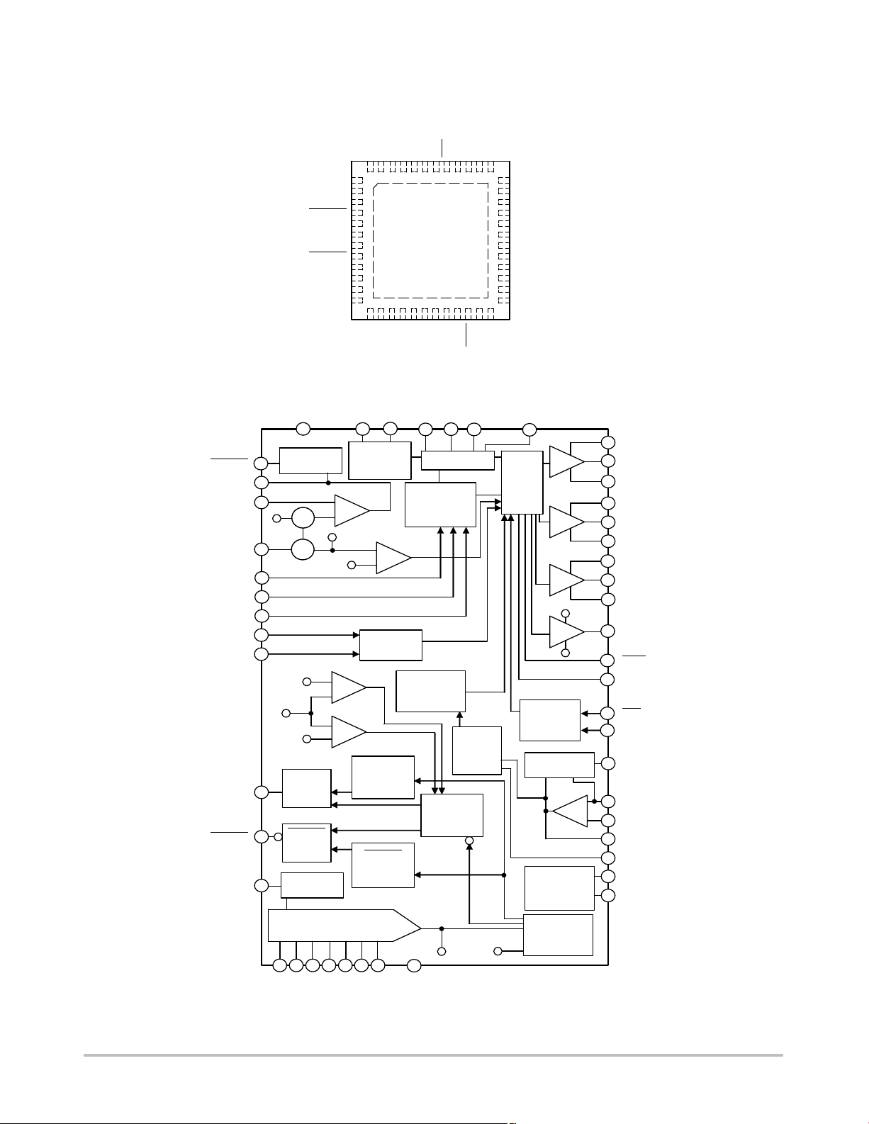
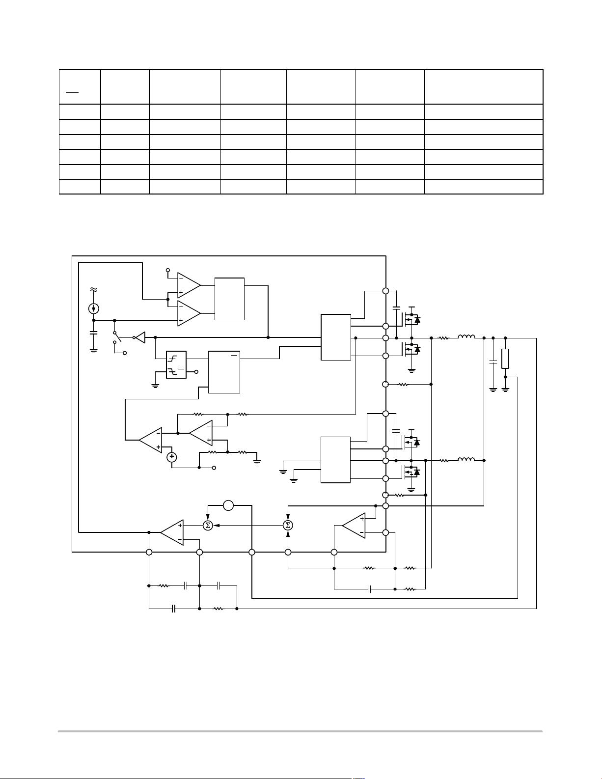
Figure 1. Functional Block Diagram
http://onsemi.com
2
Page 3

ADP3212A, NCP3218A
ABSOLUTE MAXIMUM RATINGS
Parameter Rating Unit
VCC, PV
FBRTN, PGND1, PGND2 −0.3 to +0.3 V
BST1, BST2, DRVH1, DRVH2
DC
t < 200 ns
BST1 to PVCC, BST2 to PV
DC
t < 200 ns
BST1 to SW1, BST2 to SW2 −0.3 to +6.0 V
SW1, SW2
DC
t < 200 ns
DRVH1 to SW1, DRVH2 to SW2 −0.3 to +6.0 V
DRVL1 to PGND1, DRVL2 to PGND2
DC
t < 200 ns
RAMP (in Shutdown) −0.3 to +22 V
All Other Inputs and Outputs −0.3 to +6.0 V
Storage Temperature Range −65 to +150 °C
Operating Ambient Temperature Range −40 to +100 °C
Operating Junction Temperature 125 °C
Thermal Impedance (qJA) 2−Layer Board
Lead Temperature
Soldering (10 sec)
Infrared (15 sec)
Stresses exceeding Maximum Ratings may damage the device. Maximum Ratings are stress ratings only. Functional operation above the
Recommended Operating Conditions is not implied. Extended exposure to stresses above the Recommended Operating Conditions may affect
device reliability.
NOTE: This device is ESD sensitive. Use standard ESD precautions when handling.
CC1
, PV
CC2
CC
−0.3 to +6.0 V
V
−0.3 to +28
−0.3 to +33
V
−0.3 to +22
−0.3 to +28
V
−1.0 to +22
−6.0 to +28
V
−0.3 to +6.0
−5.0 to +6.0
30.5 °C/W
°C
300
260
PIN ASSIGNMENT
Pin No. Mnemonic Description
1 EN Enable Input. Driving this pin low shuts down the chip, disables the driver outputs, pulls PWRGD and
2 PWRGD Power−Good Output. Open−drain output. A low logic state means that the output voltage is outside of the
3 IMON Current Monitor Output. This pin sources a current proportional to the output load current. A resistor to
4 CLKEN Clock Enable Output. Open−drain output. A low logic state enables the CPU internal PLL clock to lock to
5 FBRTN Feedback Return Input/Output. This pin remotely senses the CPU core voltage. It is also used as the
6 FB Voltage Error Amplifier Feedback Input. The inverting input of the voltage error amplifier.
7 COMP Voltage Error Amplifier Output and Frequency Compensation Point.
8 TRDET Transient Detect Output. This pin is pulled low when a load release transient is detected. During repetitive
9 VARFREQ Variable Frequency Enable Input. A high logic state enables the PWM clock frequency to vary with VID code.
10 VRTT Voltage Regulator Thermal Throttling Output. Logic high state indicates that the voltage regulator
VRTT low, and pulls CLKEN
VID DAC defined range.
FBRTN sets the current monitor gain.
the external clock.
ground return for the VID DAC and the voltage error amplifier blocks.
load transients at high frequencies, this circuit optimally positions the maximum and minimum output
voltage into a specified loadline window.
temperature at the remote sensing point exceeded a set alarm threshold level.
high.
http://onsemi.com
3
Page 4

ADP3212A, NCP3218A
PIN ASSIGNMENT
Pin No. DescriptionMnemonic
11 TTSNS Thermal Throttling Sense and Crowbar Disable Input. A resistor divider where the upper resistor is connected
12 GND Analog and Digital Signal Ground.
13 IREF
14 RPM RPM Mode Timing Control Input. A resistor between this pin to ground sets the RPM mode turn−on
15 RT Multi−phase Frequency Setting Input. An external resistor connected between this pin and GND sets the
16 RAMP PWM Ramp Slope Setting Input. An external resistor from the converter input voltage node to this pin sets
17 LLINE Output Load Line Programming Input. The center point of a resistor divider between CSREF and
18 CSREF Current Sense Reference Input. This pin must be connected to the common point of the output inductors.
19 CSSUM Current Sense Summing Input. External resistors from each switch node to this pin sum the inductor
20 CSCOMP Current Sense Compensation Point. A resistor and capacitor from this pin to CSSUM determine the gain of
21 ILIM Current Limit Setpoint. An external resistor from this pin to CSCOMP sets the current limit threshold of the
22 OD3 Multi−phase Output Disable Logic Output. This pin is actively pulled low when the APD3212A/NCP3218A
23 PWM3 Logic−Level PWM Output for phase 3. Connect to the input of an external MOSFET driver such as the
24 SWFB3 Current Balance Input for phase 3. Input for measuring the current level in phase 3. SWFB3 should be left
25 BST2 High−Side Bootstrap Supply for Phase 2. A capacitor from this pin to SW2 holds the bootstrapped voltage
26 DRVH2 High−Side Gate Drive Output for Phase 2.
27 SW2 Current Return for High−Side Gate Drive for phase 2.
28 SWFB2 Current Balance Input for phase 2. Input for measuring the current level in phase 2. SWFB2 should be left
29 DRVL2 Low−Side Gate Drive Output for Phase 2.
30 PGND Low−Side Driver Power Ground
31 DRVL1 Low−Side Gate Drive Output for Phase 1.
32 PVCC Power Supply Input/Output of Low−Side Gate Drivers.
33 SWFB1 Current Balance Input for phase 1. Input for measuring the current level in phase 1.
34 SW1 Current Return For High−Side Gate Drive for phase 1.
35 DRVH1 High−Side Gate Drive Output for Phase 1.
36 BST1 High−Side Bootstrap Supply for Phase 1. A capacitor from this pin to SW1 holds the bootstrapped voltage
37 VCC Power Supply Input/Output of the Controller.
38 PH1 Phase Number Configuration Input. Connect to VCC for 3 phase configuration.
39 PH0 Phase Number Configuration Input. Connect to GND for 1 phase configuration. Connect to VCC for
40 DPRSLP Deeper Sleep Control Input.
41 PSI Power State Indicator Input. Pulling this pin to GND forces the APD3212A/NCP3218A to operate in
42 to48VID6 to VID0 Voltage Identification DAC Inputs. When in normal operation mode, the DAC output programs the FB
to VCC, the lower resistor (NTC thermistor) is connected to GND, and the center point is connected to this
pin and acts as a temperature sensor half bridge. Connecting TTSNS to GND disables the thermal throttling
function and disables the crowbar, or Overvoltage Protection (OVP), feature of the chip.
This pin sets the internal bias currents. A 80 kW resistor is connected from this pin to ground.
threshold voltage.
oscillator frequency of the device when operating in multi−phase PWM mode threshold of the converter.
the slope of the internal PWM stabilizing ramp used for phase−current balancing.
CSCOMP is connected to this pin to set the load line slope.
The node is shorted to GND through an internal switch when the chip is disabled to provide soft stop
transient control of the converter output voltage.
currents to provide total current information.
the current−sense amplifier and the positioning loop response time.
converter.
enters single−phase mode or during shutdown. Connect this pin to the SD inputs of the Phase−3 MOSFET
drivers.
ADP3611.
open for 1 or 2 phase configuration.
while the high−side MOSFET is on.
open for 1 phase configuration.
while the high−side MOSFET is on.
multi−phase configuration.
single−phase mode.
regulation voltage from 0.3 V to 1.5 V (see Table 3).
http://onsemi.com
4
Page 5

ADP3212A, NCP3218A
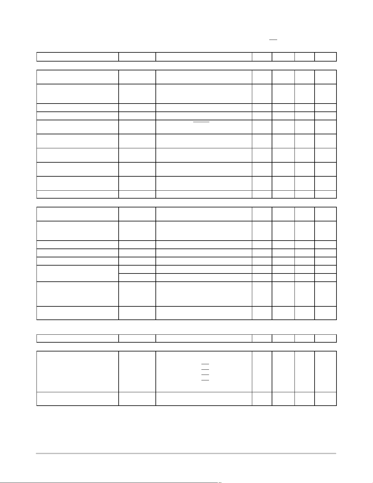
ELECTRICAL CHARACTERISTICS
VCC = PVCC = 5.0 V, FBRTN = PGND = GND = 0 V, H = 5.0 V, L = 0 V, EN = VARFREQ = H, DPRSLP = L, PSI = 1.05 V,
= V
V
VID
VOLTAGE CONTROL − VOLTAGE ERROR AMPLIFIER (VEAMP)
FB, LLINE Voltage Range (Note 2)
FB, LLINE Offset Voltage (Note 2) V
LLINE Bias Current I
FB Bias Current I
LLINE Positioning Accuracy VFB − V
COMP Voltage Range (Note 2) V
COMP Current I
COMP Slew Rate SR
Gain Bandwidth (Note 2) GBW Non−inverting unit gain configuration,
VID DAC VOLTAGE REFERENCE
VDAC Voltage Range (Note 2)
VDAC Accuracy VFB − V
VDAC Differential Non−linearity
(Note 2)
VDAC Line Regulation ΔV
VDAC Boot Voltage V
Soft−Start Delay (Note 2) t
Soft−Start Time t
Boot Delay t
VDAC Slew Rate (Note 2) Soft−Start
FBRTN Current I
VOLTAGE MONITORING and PROTECTION − POWER GOOD
CSREF Undervoltage Threshold
CSREF Overvoltage Threshold V
1. All limits at temperature extremes are guaranteed via correlation using standard statistical quality control (SQC).
2. Guaranteed by design or bench characterization, not production tested.
3. Based on bench characterization data.
4. Timing is referenced to the 90% and 10% points, unless otherwise noted.
= 1.2000 V, TA = −40°C to 100°C, unless otherwise noted. (Note 1) Current entering a pin (sink current) has a positive sign.
DAC
Parameter
Symbol Conditions Min Typ Max Units
VFB, V
OSVEA
LLINE
COMP
COMP
LLINE
FB
COMP
Relative to CSREF = VDAC −200 +200 mV
Relative to CSREF = VDAC −0.5 +0.5 mV
−100 +100 nA
−1.0 +1.0
Measured on FB relative to V
VID
forced 80 mV below CSREF
VID
, LLINE
−77.5 −80 −82.5 mV
0.85 4.0 V
COMP = 2.0 V, CSREF = VDAC
FB forced 200 mV below CSREF
FB forced 200 mV above CSREF
C
= 10 pF, CSREF = VDAC,
COMP
Open loop configuration
FB forced 200 mV below CSREF
FB forced 200 mV above CSREF
−0.75
6.0
15
−20
20 MHz
= 1 kW
R
FB
See VID table 0 1.5 V
Measured on FB (includes offset),
VID
relative to V
V
VID
T = −10°C to 100°C
V
VID
T = −40°C to 100°C
V
VID
T = −10°C to 100°C
V
VID
T = −40°C to 100°C
VID
= 0.5000 V to 1.5000 V,
= 0.5000 V to 1.5000 V,
= 0.3000 V to 0.4875 V,
= 0.3000 V to 0.4875 V,
−7.5
−9.0
−9.0
−10
−1.0 +1.0 LSB
FB
BOOTFB
DSS
SS
BOOT
VCC = 4.75 V to 5.25 V 0.001 %
Measured during boot delay period 1.100 V
Measured from EN pos edge to
200
FB = 50 mV
Measured from FB = 50 mV to FB settles
1.4 ms
to 1.1 V within 5%
Measured from FB settling to 1.1 V within
5% to CLKEN
neg edge
60
0.0625
Non−LSB VID step, DPRSLP = H, Slow
0.25
C4 Entry/Exit
Non−LSB VID step, DPRSLP = L, Fast
1.0
C4 Exit
LSB VID step, DVID transition
GPU Mode, Non−LSB VID step, Fast
0.4
1.0
Entry/Exit
FBRTN
V
UVCSREF
OVCSREF
Relative to nominal VDAC voltage −240 −300 −360 mV
Relative to nominal VDAC voltage,
T = −10°C to 100°C
T = −40°C to 100°C
150
140
−90 −200
200
200
mA
mA
V/ms
mV
+7.5
+9.0
+9.0
+10
ms
ms
LSB/
ms
mA
mV
250
250
http://onsemi.com
5
Page 6
ADP3212A, NCP3218A
ELECTRICAL CHARACTERISTICS
VCC = PVCC = 5.0 V, FBRTN = PGND = GND = 0 V, H = 5.0 V, L = 0 V, EN = VARFREQ = H, DPRSLP = L, PSI = 1.05 V,
= V
V
VID
VOLTAGE MONITORING and PROTECTION − POWER GOOD
CSREF Crowbar Voltage
Threshold
CSREF Reverse Voltage
Threshold
PWRGD Low Voltage V
PWRGD High, Leakage Current I
PWRGD Startup Delay T
PWRGD Latchoff Delay T
PWRGD Propagation Delay
(Note 3)
Crowbar Latchoff Delay (Note 2) T
PWRGD Masking Time Triggered by any VID change or OCP
CSREF Soft−Stop Resistance EN = L or latchoff condition 70
CURRENT CONTROL − CURRENT−SENSE AMPLIFIER (CSAMP)
CSSUM, CSREF Common−Mode
Range (Note 2)
CSSUM, CSREF Offset Voltage V
CSSUM Bias Current I
CSREF Bias Current I
CSCOMP Voltage Range (Note 2) Voltage range of interest 0.05 2.0 V
CSCOMP Current
CSCOMP Slew Rate (Note 2) C
Gain Bandwidth (Note 2) GBW
CURRENT MONITORING and PROTECTION
CURRENT REFERENCE
I
REF
CURRENT LIMITER (OCP)
Current Limit (OCP) Threshold
Current Limit Latchoff Delay Measured from OCP event to PWRGD
1. All limits at temperature extremes are guaranteed via correlation using standard statistical quality control (SQC).
2. Guaranteed by design or bench characterization, not production tested.
3. Based on bench characterization data.
4. Timing is referenced to the 90% and 10% points, unless otherwise noted.
= 1.2000 V, TA = −40°C to 100°C, unless otherwise noted. (Note 1) Current entering a pin (sink current) has a positive sign.
DAC
Parameter UnitsMaxTypMinConditionsSymbol
V
CBCSREF
V
RVCSREF
PWRGD
PWRGD
SSPWRGD
LOFFPWRGD
T
PDPWRGD
LOFFCB
Relative to FBRTN 1.5 1.55 1.6 V
Relative to FBRTN, latchoff mode
CSREF is falling
CSREF is rising
I
PWRGD(SINK)
V
PWRDG
= 4 mA 85 250 mV
= 5.0 V 1.0
Measured from CLKEN neg edge to
−350 −300
−75 −10
9.0 ms
PWRGD pos edge
Measured from Out−off−Good−Window
9.0
event to Latchoff (switching stops)
Measured from Out−off−Good−Window
200 ns
event to PWRGD neg edge
Measured from Crowbar event to latchoff
200 ns
(switching stops)
100
event
Voltage range of interest 0 2.0 V
BCSSUM
I
CSCOMPsource
I
CSCOMPsink
Voltage V
OSCSA
BCSREF
CSA
REF
V
LIMTH
CSREF – CSSUM, TA = 25°C
T
= −10°C to 85°C
A
TA = −40°C to 85°C
CSSUM forced 200 mV below CSREF −750
CSSUM forced 200 mV above CSREF 1.0 mA
= 10 pF, CSREF = VDAC,
CSCOMP
Open loop configuration
CSSUM forced 200 mV below CSREF
CSSUM forced 200 mV above CSREF
Non−inverting unit gain configuration
= 1 kW
R
FB
R
= 80 kW to set I
REF
REF
= 20 mA
Measured from CSCOMP to CSREF,
= 1.5 kW,
R
LIM
3−ph configuration, PSI = H
3−ph configuration, PSI = L
2−ph configuration, PSI = H
2−ph configuration, PSI
= L
1−ph configuration
−0.5
−1.7
−1.9
−50 +50 nA
−2.0 +2.0
20
−20
20 MHz
1.55 1.6 1.65 V
−80
−22
−80
−35
−75
−90
−30
−90
−45
−90
150
de−assertion
+0.5
+1.7
+1.9
−100
−38
−100
−55
−105
mV
mA
ms
ms
W
mV
mA
mA
V/ms
mV
ms
http://onsemi.com
6
Page 7
ADP3212A, NCP3218A
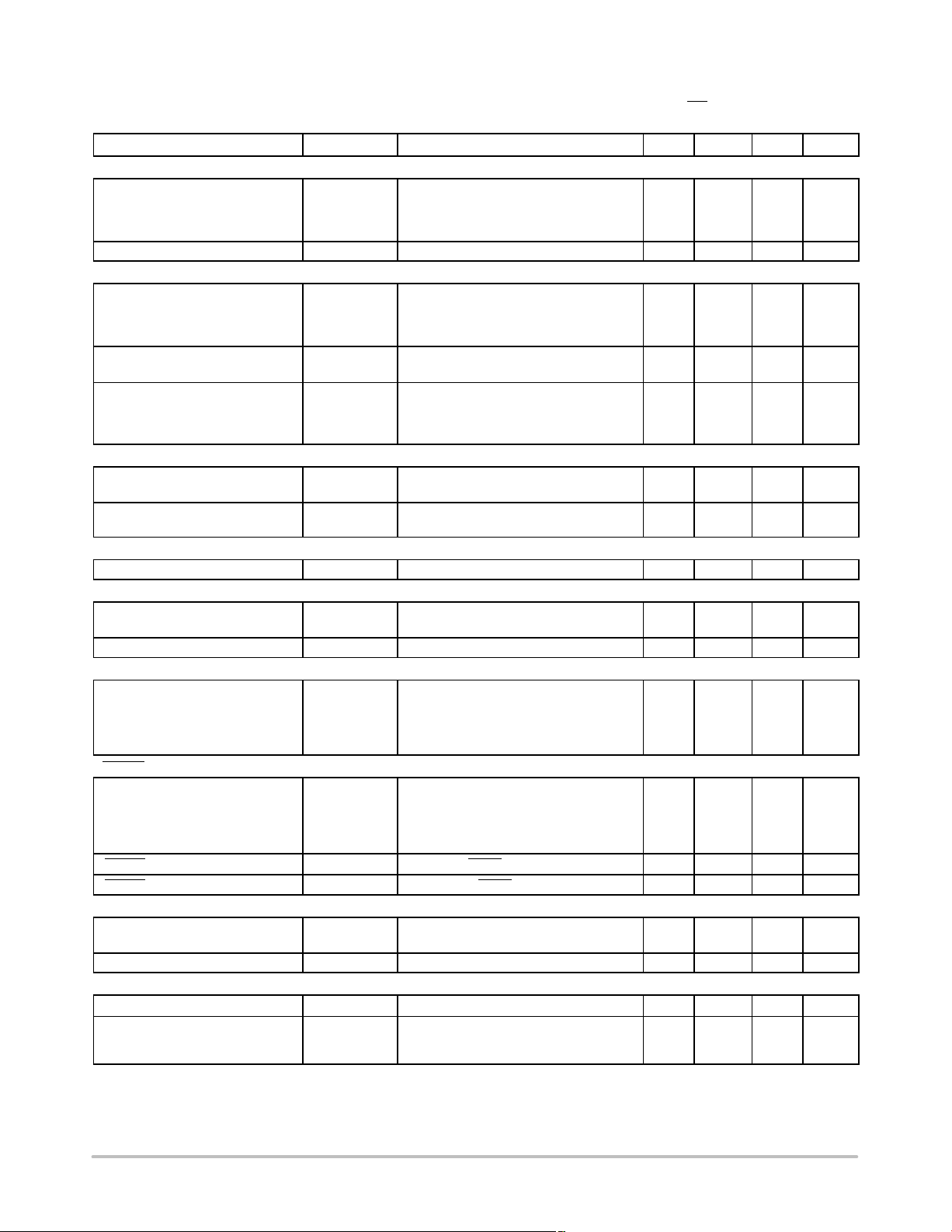
ELECTRICAL CHARACTERISTICS
VCC = PVCC = 5.0 V, FBRTN = PGND = GND = 0 V, H = 5.0 V, L = 0 V, EN = VARFREQ = H, DPRSLP = L, PSI = 1.05 V,
= V
V
VID
CURRENT MONITOR
Current Gain Accuracy
I
MON
PULSE WIDTH MODULATOR − CLOCK OSCILLATOR
RT Voltage
PWM Clock Frequency Range
(Note 2)
PWM Clock Frequency f
RAMP GENERATOR
RAMP Voltage
RAMP Current Range (Note 2) I
PWM COMPARATOR
PWM Comparator Offset (Note 2)
RPM COMPARATOR
RPM Current
RPM Comparator Offset (Note 2) V
EPWM CLOCK SYNC
Trigger Threshold (Note 2)
TRDET
Trigger Threshold (Note 2) Relative to COMP sampled T
TRDET Low Voltage (Note 2) V
TRDET Leakage Current I
SWITCH AMPLIFIER
SW Common Mode Range
(Note 2)
SWFB Input Resistance R
ZERO CURRENT SWITCHING COMPARATOR
SW ZCS Threshold
Masked Off−Time t
1. All limits at temperature extremes are guaranteed via correlation using standard statistical quality control (SQC).
2. Guaranteed by design or bench characterization, not production tested.
3. Based on bench characterization data.
4. Timing is referenced to the 90% and 10% points, unless otherwise noted.
= 1.2000 V, TA = −40°C to 100°C, unless otherwise noted. (Note 1) Current entering a pin (sink current) has a positive sign.
DAC
Parameter UnitsMaxTypMinConditionsSymbol
Clamp Voltage V
I
MON/ILIM
MAXMON
V
RT
f
CLK
CLK
V
RAMP
RAMP
V
OSRPM
I
RPM
OSRPM
LTRDET
HTRDET
V
SW(X)CM
SW(X)
V
DCM(SW1)
OFFMSKD
Measured from I
I
= −20 mA
LIM
= −10 mA
I
LIM
= −5 mA
I
LIM
Relative to FBRTN, ILIMP = −30 mA
LIM
to I
MON
3.7
3.6
3.5
4.0
4.0
4.0
1.0 1.16 V
VARFREQ = high, RT = 125 kW,
V
= 1.5000 V
VID
VARFREQ = low
See also VRT(V
) formula
VID
1.125
0.9
1.25
1.0
Operation of interest 0.3 3.0 MHz
TA = +25°C, V
= 72 kW
R
T
= 120 kW
R
T
= 180 kW
R
T
EN = high, I
EN = low
EN = high
EN = low, RAMP = 19 V
V
− V
RAMP
V
= 1.2 V, RT = 215 kW
VID
See also I
V
− (1 + V
COMP
Relative to COMP sampled T
earlier
3−phase configuration
2−phase configuration
1−phase configuration
earlier
3−phase configuration
2−phase configuration
1−phase configuration
Logic low, I
Logic high, V
VID
RAMP
COMP
RPM(RT
RPMTH
TRDETsink
TRDET
= 1.2000 V
= 60 mA
900
700
300
0.9 1.0
1200
800
400
V
IN
1.0
−1.0
±3.0 mV
−5.5
) formula
) ±3.0 mV
time
CLK
350
400
450
time
CLK
−450
−500
−600
= 4 mA 30 300 mV
= VCC 3.0
Operation of interest for current sensing −600 +200 mV
SWX = 0 V, SWFB = 0 V 20 35 50
DCM mode, DPRSLP = 3.3 V −3.0 mV
Measured from DRVH1 neg edge to
600 ns
DRVH1 pos edge at operation max
frequency
4.3
4.4
4.5
1.375
1.1
1500
900
500
1.1 V
100
+1.0
−
V
kHz
mA
mA
mV
mV
mA
kW
http://onsemi.com
7
Page 8
ADP3212A, NCP3218A
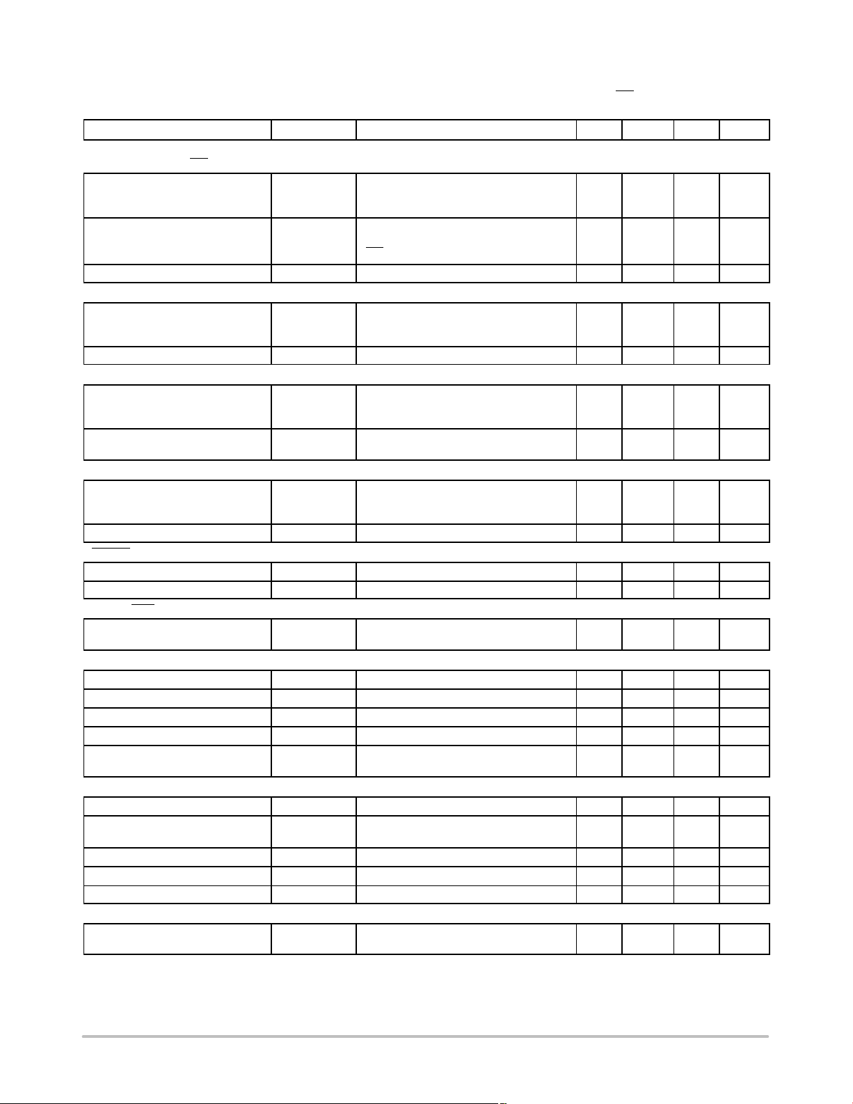
ELECTRICAL CHARACTERISTICS
VCC = PVCC = 5.0 V, FBRTN = PGND = GND = 0 V, H = 5.0 V, L = 0 V, EN = VARFREQ = H, DPRSLP = L, PSI = 1.05 V,
= V
V
VID
SYSTEM I/O BUFFERS
VID[6:0], DPRSLP, PSI
Input Voltage Refers to driving signal level
Input Current V = 0.2 V, VID[6:0], DPRSLP
VID Delay Time (Note 2) Any VID edge to FB change 10% 200 ns
VARFREQ
Input Voltage
Input Current 1.0
EN INPUT
Input Voltage
Input Current EN = L or EN = H (static)
PH1, PH0 INPUTS
Input Voltage
Input Current 1.0
CLKEN OUTPUT
Output Low Voltage
Output High, Leakage Current Logic high, V
PWM3, OD3 OUTPUTS
Output Voltage
THERMAL MONITORING and PROTECTION
TTSNS Voltage Range (Note 2)
TTSNS Threshold VCC = 5.0 V, TTSNS is falling 2.45 2.5 2.55 V
TTSNS Hysteresis 50 95 mV
TTSNS Bias Current TTSNS = 2.6 V −2.0 2.0
VRTT Output Voltage V
SUPPLY
Supply Voltage Range
Supply Current EN = high
VCC OK Threshold V
VCC UVLO Threshold V
VCC Hysteresis (Note 2) 250 mV
HIGH−SIDE MOSFET DRIVER
Pullup Resistance, Sourcing
Current (Note 3)
1. All limits at temperature extremes are guaranteed via correlation using standard statistical quality control (SQC).
2. Guaranteed by design or bench characterization, not production tested.
3. Based on bench characterization data.
4. Timing is referenced to the 90% and 10% points, unless otherwise noted.
= 1.2000 V, TA = −40°C to 100°C, unless otherwise noted. (Note 1) Current entering a pin (sink current) has a positive sign.
DAC
Parameter UnitsMaxTypMinConditionsSymbol
INPUTS
Logic low
Logic high
(active pulldown to GND)
PSI
(active pullup to VCC)
2.0
1.0
−2.0
0.3
Refers to driving signal level
Logic low
Logic high
4.0
0.7
Refers to driving signal level
Logic low
0.5
Logic high 1.7
10
0.8 V < EN < 1.6 V (during transition)
−70
Refers to driving signal level
Logic low
Logic high
Logic low, I
Logic low, I
Logic high, I
2.0
= 4 mA 60 200 mV
sink
= VCC 0.1
CLKEN
= 400 mA
SINK
SOURCE
= −400 mA
4.0
10
5.0
0.5
500 mV
0 5.0 V
VRTT
V
CC
CCOK
CCUVLO
Logic low, I
Logic high, I
VRTT(SINK)
VRTT(SOURCE)
= 400 mA
= −400 mA
4.5
10
5.0
4.5 5.5 V
7
EN = 0 V
10
VCC is rising 4.4 4.5 V
VCC is falling 4.0 4.15 V
500 mV
10
50
BST = PVCC 1.25 3.3
V
mA
V
mA
V
nA
mA
V
mA
mA
V
mA
V
mA
mA
W
http://onsemi.com
8
Page 9
ADP3212A, NCP3218A
ELECTRICAL CHARACTERISTICS
VCC = PVCC = 5.0 V, FBRTN = PGND = GND = 0 V, H = 5.0 V, L = 0 V, EN = VARFREQ = H, DPRSLP = L, PSI = 1.05 V,
= V
V
VID
HIGH−SIDE MOSFET DRIVER
Pulldown Resistance, Sinking
Current (Note 3)
Transition Times tr
Dead Delay Times tpdh
BST Quiescent Current EN = L (Shutdown)
LOW−SIDE MOSFET DRIVER
Pullup Resistance, Sourcing
Current (Note 3)
Pulldown Resistance, Sinking
Current (Note 3)
Transition Times tr
Propagation Delay Times tpdh
SW Transition Timeout t
SW Off Threshold V
PVCC Quiescent Current EN = L (Shutdown)
BOOTSTRAP RECTIFIER SWITCH
On Resistance (Note 3)
1. All limits at temperature extremes are guaranteed via correlation using standard statistical quality control (SQC).
2. Guaranteed by design or bench characterization, not production tested.
3. Based on bench characterization data.
4. Timing is referenced to the 90% and 10% points, unless otherwise noted.
= 1.2000 V, TA = −40°C to 100°C, unless otherwise noted. (Note 1) Current entering a pin (sink current) has a positive sign.
DAC
Parameter UnitsMaxTypMinConditionsSymbol
BST = PVCC 0.8 2.0
DRVH
tf
DRVH
DRVH
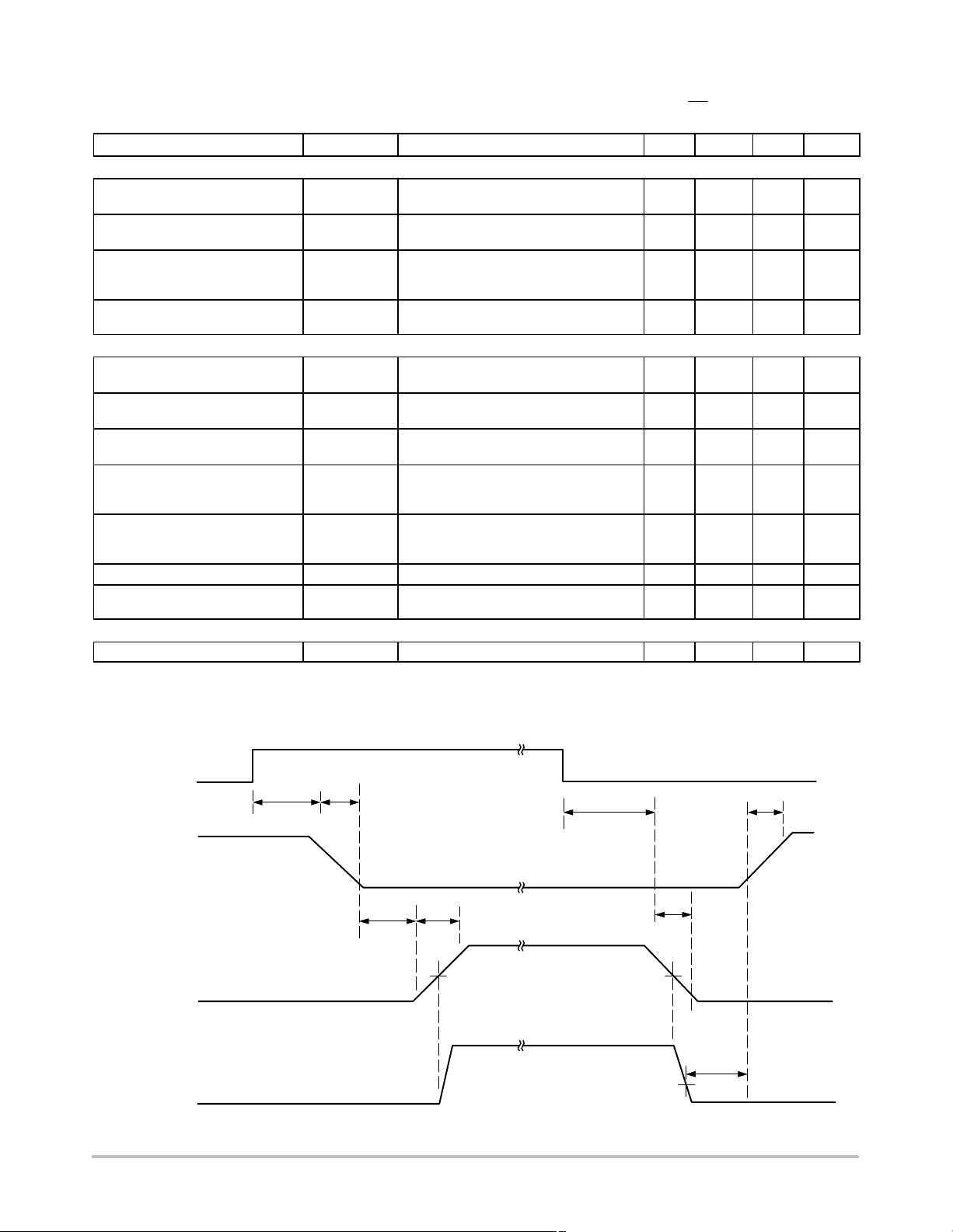
BST = PVCC, CL = 3 nF, Figure 2
BST = PVCC, CL = 3 nF, Figure 2
BST = PVCC, Figure 2
T = −10°C to 100°C
28 32 36
15
13
T = −40°C to 100°C
1.0
EN = H, no switching
200
0.88 2.8
0.65 1.7
DRVL
tf
DRVL
DRVL
TOSW
OFFSW
CL = 3 nF, Figure 2
C
= 3 nF, Figure 2
L
CL = 3 nF, Figure 2
T = −10°C to 100°C
T = −40°C to 100°C
DRVH = L, SW = 2.5 V
T = −10°C to 100°C
T = −40°C to 100°C
85
85
15
14
11
12
250
250
1.6 V
1.0
EN = H, no switching
170
EN = L or EN = H and DRVL = H 5.0 7.0 12
35
31
50
10
35
35
30
40
300
450
10
W
ns
ns
mA
W
W
ns
ns
ns
mA
W
IN
tpdl
DRVL
DRVL
DRVH
(WITH RESPECT TO SW)
SW
tpdh
tf
DRVL
tr
DRVH
DRVH
V
TH
Figure 2. Timing Diagram (Note 4)
http://onsemi.com
9
tpdl
DRVH
V
TH
1.0 V
tf
tpdh
tr
DRVL
DRVH
DRVL
Page 10
3.3 V
EN
PWRGD
1 kW
ADP3212A, NCP3218A
TEST CIRCUITS
7−BIT CODE
48
1
GND
80 kW
VID1
VID2
VID0
IMON
CLKEN
FBRTN
FB
COMP
TRDET
VARFREQ
VRTT
TTSNS
IREF
RPMRTRAMP
VID5
VID4
VID3
ADP3212A
LLINE
CSREF
VID6
CSSUM
PSI
PH1
PH2
DPRSLP
SWFB1
PVCC
DRVL1
PGND
DRVL2
SWFB2
CSCOMP
ILIM
OD3
20 kW
100 nF
VCC
SW1
SW2
PWM3
SWFB3
5 V
BST1
DRVH1
DRVH2
BST2
39 kW
1 kW
1.0 V
5.0 V
100 nF
37
20
19
18
12
VCC
CSCOMP
CSSUM
CSREF
GND
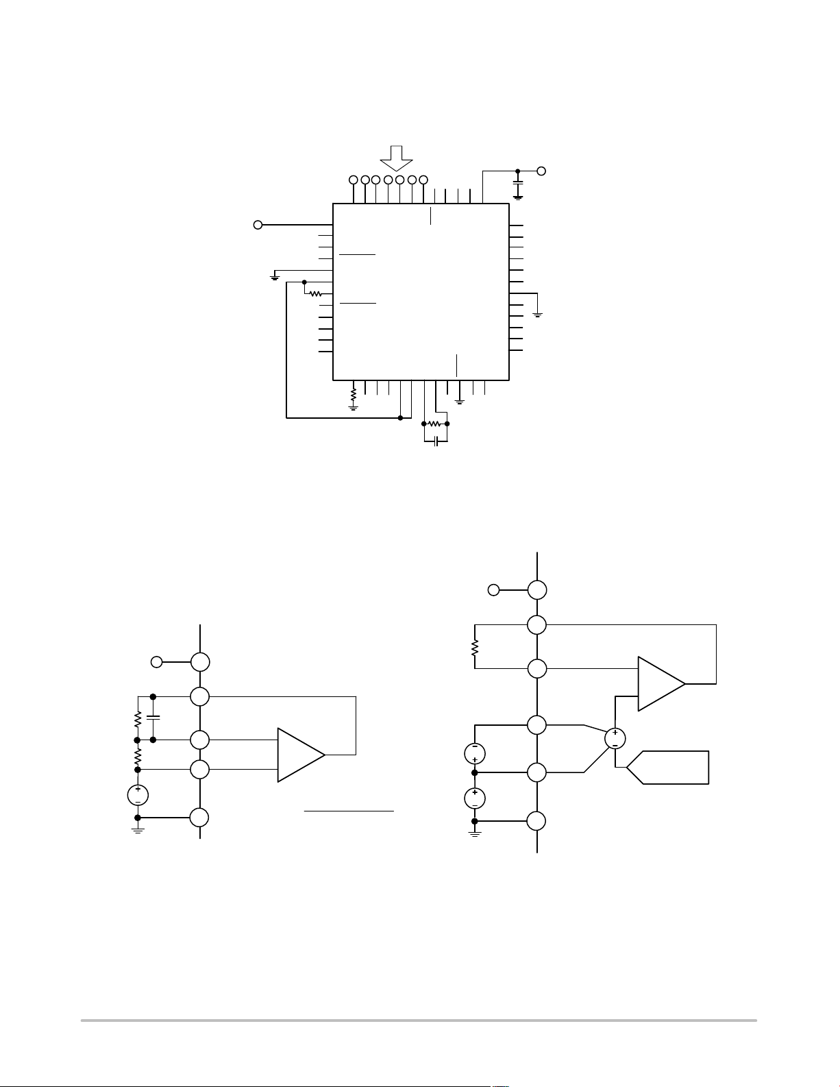
Figure 3. Closed−Loop Output Voltage Accuracy
5.0 V
ADP3212A
−
+
CSCOMP * 1.0 V
V
+
OS
40 V
10 kW
DV
1.0 V
VCC
37
COMP
7
FB
6
LLINE
17
CSREF
18
GND
12
DVFB+ FBDV+ DV * FB
ADP3212A
−
+
VID DAC
DV+0mV
Figure 4. Current Sense Amplifier, V
OS
http://onsemi.com
Figure 5. Positioning Accuracy
10
Page 11
ADP3212A, NCP3218A
TYPICAL PERFORMANCE CHARACTERISTICS
V
= 1.5 V, TA = 20°C to 100°C, unless otherwise noted.
VID
400
350
300
250
200
150
FREQUENCY (kHz)
100
PER PHASE SWITCHING
50
0
VARFREQ = 0 V
VARFREQ = 5 V
VID OUTPUT VOLTAGE (V)
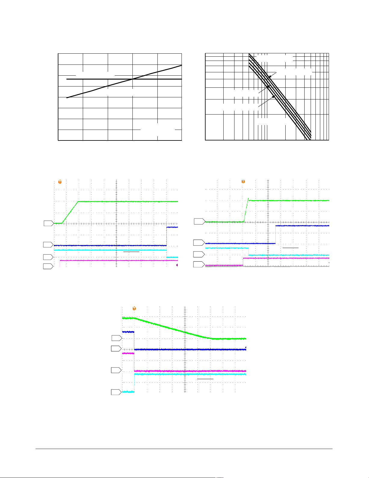
Figure 6. Switching Frequency vs. VID Output
Voltage in PWM Mode
Output Voltage
1
RT = 187 kW
2 Phase Mode
1000
VID = 0.8125 V
SWITCHING FREQUENCY (kHz)
100
1.501.251.000.750.500.25
Figure 7. Per Phase Switching Frequency vs.
1
VID = 1.4125 V
VID = 1.2125 V
VID = 1.1 V
VID = 0.6125 V
100010010
Rt RESISTANCE (kW)
RT Resistance
Output Voltage
PWRGD
2
3
4
1: 0.5 V/div
2: 2 V/div
3: 5 V/div
4: 5 V/div
PWRGD
CLKEN
1 ms/div
EN
GPU Mode
2
3
4
1: 0.5 V/div
2: 2 V/div
3: 5 V/div
4: 5 V/div
EN
4 ms/div
CLKEN
CPU Mode
Figure 8. Startup in GPU Mode Figure 9. Startup in CPU Mode
Output Voltage
1
2
3
4
1: 0.5 V/div
2: 2 V/div
PWRGD
EN
3: 2 V/div
4: 2 V/div
CLKEN
200 ms/div
1 A Load
Figure 10. Shutdown
http://onsemi.com
11
Page 12
ADP3212A, NCP3218A
TYPICAL PERFORMANCE CHARACTERISTICS
V
= 1.5 V, TA = 20°C to 100°C, unless otherwise noted.
VID
1
2
3
4
SW1
SW2
SW3
DPRSLP
1: 10 V/div
2: 10 V/div
3: 10 V/div
4: 2 V/div
4 ms/div
1
2
3
4
PSI
1: 10 V/div
2: 10 V/div
3: 10 V/div
4: 0.5 V/div
SW1
SW2
SW3
4 ms/div
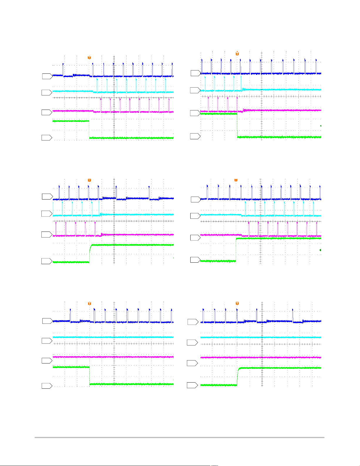
Figure 11. DPRSLP Transition with PSI = High Figure 12. PSI Transition with DPRSLP = Low
SW1
SW1
1
SW2
2
SW3
3
1
SW2
2
SW3
3
4
DPRSLP
1: 10 V/div
2: 10 V/div
3: 10 V/div
4: 2 V/div
4
4 ms/div
PSI
1: 10 V/div
2: 10 V/div
3: 10 V/div
4: 0.5 V/div
4 ms/div
Figure 13. DPRSLP Transition with PSI = High Figure 14. PSI Transition with DPRSLP = Low
1
2
3
4
1: 10 V/div
2: 10 V/div
SW1
SW2
SW3
3: 10 V/div
4: 2 V/div
DPRSLP
4 ms/div
1
2
3
4
1: 10 V/div
2: 10 V/div
SW2
SW3
3: 10 V/div
4: 2 V/div
DPRSLP
4 ms/div
Figure 15. DPRSLP Transition with PSI = Low Figure 16. DPRSLP Transition with PSI = Low
SW1
http://onsemi.com
12
Page 13

ADP3212A, NCP3218A
Theory of Operation
The APD3212A/NCP3218A combines multi−mode
Pulse−Width Modulated (PWM) control and Ramp−Pulse
Modulated (RPM) control with multi−phase logic outputs
for use in single−, dual−phase, or triple−phase synchronous
buck CPU core supply power converters. The internal 7−bit
VID DAC conforms to the Intel IMVP−6.5 specifications.
Multi−phase operation is important for producing the high
currents and low voltages demanded by today’s
microprocessors. Handling high currents in a single−phase
converter would put too high of a thermal stress on system
components such as the inductors and MOSFETs.
The multimode control of the APD3212A/NCP3218A is
a stable, high performance architecture that includes
• Current and thermal balance between phases.
• High speed response at the lowest possible switching
frequency and minimal count of output decoupling
capacitors.
• Minimized thermal switching losses due to lower
frequency operation.
• High accuracy load line regulation.
• High current output by supporting 2−phase or 3−phase
operation.
• Reduced output ripple due to multi−phase ripple
cancellation.
• High power conversion efficiency with heavy and light
loads.
• Increased immunity from noise introduced by PC board
layout constraints.
• Ease of use due to independent component selection.
• Flexibility in design by allowing optimization for either
low cost or high performance.
Number of Phases
The number of operational phases can be set by the user.
Tying the PH1 pin to the GND pin forces the chip into
single−phase operation. Tying PH0 to GND and PH1 to
VCC forces the chip into 2−phase operation. Tying PH0 and
PH1 to VCC forces the chip in 3−phase operation. PH0 and
PH1 should be hard wired to VCC or GND. The
APD3212A/NCP3218A switches between single phase and
multi−phase operation with PSI
power conversion efficiency. Table 1 summarizes PH0 and
PH1.
Table 1. PHASE NUMBER CONFIGURATION
PH0 PH1 Number of Phases Configured
0 0 1
1 0 1 (GPU Mode)
0 1 2
1 1 3
In mulit−phase configuration, the timing relationship
between the phases is determined by internal circuitry that
and DPRSLP to optimize
monitors the PWM outputs. Because each phase is
monitored independently, operation approaching 100%
duty cycle is possible. In addition, more than one output can
be active at a time, permitting overlapping phases.
Operation Modes
The number of phases can be static (see the Number of
Phases section) or dynamically controlled by system signals
to optimize the power conversion efficiency with heavy and
light loads.
If APD3212A/NCP3218A is configured for mulit−phase
configuration, during a VID transient or with a heavy load
condition (indicated by DPRSLP being low and PSI
high), the APD3212A/NCP3218A runs in multi−phase,
interleaved PWM mode to achieve minimal V
voltage ripple and the best transient performance possible. If
the load becomes light (indicated by PSI
DPRSLP being high), APD3212A/NCP3218A switches to
single−phase mode to maximize the power conversion
efficiency.
In addition to changing the number of phases, the
APD3212A/NCP3218A is also capable of dynamically
changing the control method. In dual−phase operation, the
APD3212A/NCP3218A runs in PWM mode, where the
switching frequency is controlled by the master clock. In
single−phase operation (commanded by the DPRSLP high
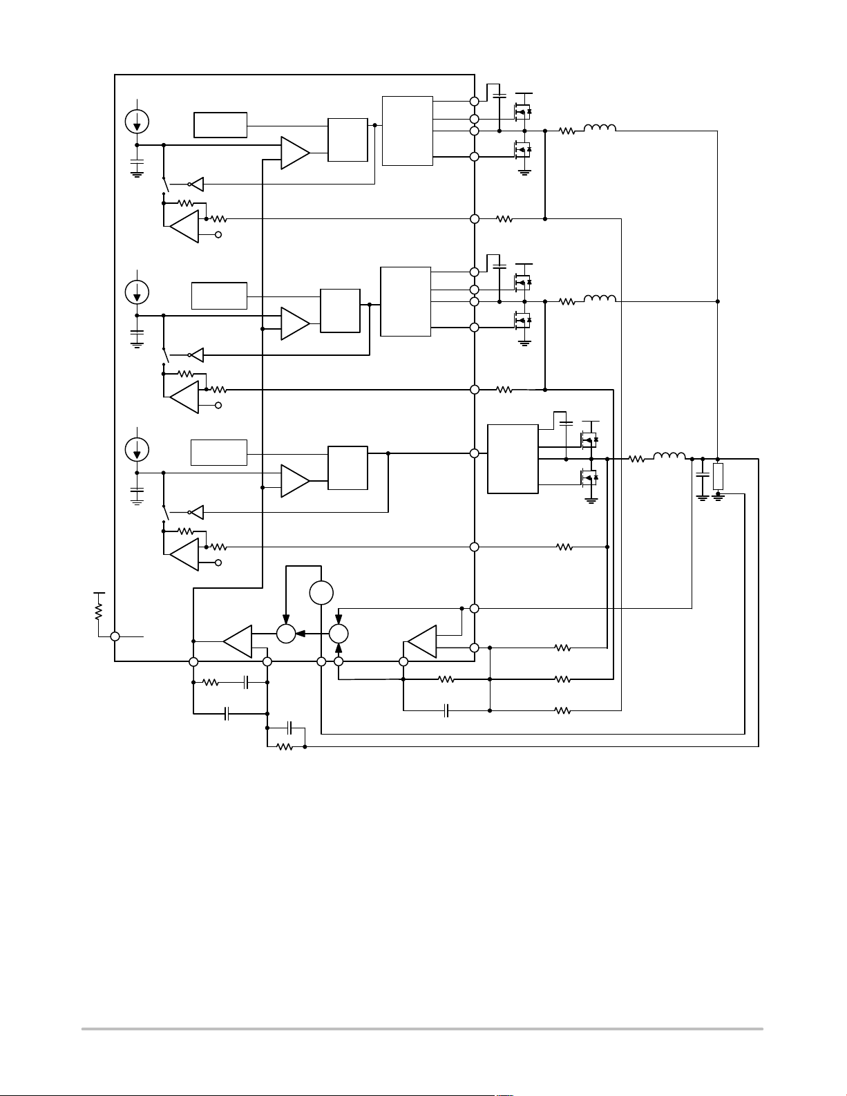
state), the APD3212A/NCP3218A runs in RPM mode,
where the switching frequency is controlled by the ripple
voltage appearing on the COMP pin. In RPM mode, the
DRVH1 pin is driven high each time the COMP pin voltage
rises to a voltage limit set by the VID voltage and an external
resistor connected between the RPM pin and GND. In RPM
mode, the APD3212A/NCP3218A turns off the low−side
(synchronous rectifier) MOSFET when the inductor current
drops to 0. Turning off the low−side MOSFETs at the zero
current crossing prevents reversed inductor current build up
and breaks synchronous operation of high− and low−side
switches. Due to the asynchronous operation, the switching
frequency becomes slower as the load current decreases,
resulting in good power conversion efficiency with very
light loads.
Table 2 summarizes how the APD3212A/NCP3218A
dynamically changes the number of active phases and
transitions the operation mode based on system signals and
operating conditions.
GPU Mode
The APD3212A/NCP3218A can be used to power
IMVP−6.5 GMCH. To configure the APD3212A/NCP3218A
in GPU, connect PH1 to VCC and connect PH0 to GND. In
GPU mode, the APD3212A/NCP3218A operates in single
phase only. In GPU mode, the boot voltage is disabled. During
startup, the output voltage ramps up to the programmed VID
voltage. There is no other difference between GPU mode and
normal CPU mode.
being low or
CORE
being
output
http://onsemi.com
13
Page 14
ADP3212A, NCP3218A
Table 2. PHASE NUMBER AND OPERATION MODES (Note 1)
VID Transition
No. DPRSLP
PSI
(Note 2)
Current Limit
* * Ye s * N [3,2 or 1] N PWM, CCM only
1 0 No * N [3,2 or 1] N PWM, CCM only
0 0 No No * 1 PWM, CCM only
0 0 No Yes N [3,2 or 1] N PWM, CCM only
* 1 No No * 1 RPM, automatic CCM/DCM
* 1 No Yes * 1 PWM, CCM only
1. * = Don’t Care.
2. VID transient period is the time following any VID change, including entry into and exit from deeper sleep mode. The duration of VID transient
period is the same as that of PWRGD masking time.
3. CCM stands for continuous current mode, and DCM stands for discontinuous current mode.
No. of Phases
Selected by
the User
No. of Phases
in Operation
Operation Modes
(Note 3)
IR = AR x I
C
R
RAMP
1 V
COMP
30 mV
VRMP
400 ns
R
A
C
FB
FLIP−FLOP
FLIP−FLOP
Q
Q
R2 R1
R2
FB
C
A
R
S
RD
+
+
C
S
RD
1 V
VDC
+
B
FB
Q
Q
R1
–
V
CS
FBRTN
LLINE
GATE DRIVER
IN
DCM
GATE DRIVER
IN
DCM
–
+
CSCOMP
BST
DRVH
SW
DRVL
BST
DRVH
SW
DRVL
BST1
DRVH1
SW1
DRVL1
SWFB1
BST2
DRVH2
SW2
DRVL2
SWFB2
CSREF
CSSUM
R
CS
C
CS
VCC
100 W
VCC
100 W
R
R
PH
PH
R
L
I
LOAD
L
R
I
Figure 17. Single−Phase RPM Mode Operation
http://onsemi.com
14
Page 15
ADP3212A, NCP3218A
IR = AR x I
C
R
A
D
IR = AR x I
C
R
A
D
IR = AR x I
C
R
RAMP
RAMP
RAMP
Clock
Oscillator
−
+
0.2 V
Clock
Oscillator
−
+
0.2 V
Clock
Oscillator
Gate Driver
Flip−Flop
QS
+
−
+
−
+
−
RD
Flip−Flop
Q
S
RD
Flip−Flop
S
RD
Q
DRVH
IN
Gate Driver
DRVH
IN
DRVL
BST
SW
DRVL
BST
SW
BST1
DRVH1
SW1
DRVL1
SWFB1
BST2
DRVH2
SW2
DRVL2
SWFB2
PWM3
VCC
100 W
VCC
100 W
Gate Driver
BST
DRVH
IN
SW
DRVL
L
R
L
L
R
L
VCC
L
R
L
LOAD
COMP
−
+
0.2 V
+
DAC
_
+
+
S
FB
−
R
A
C
A
C
FB
+
FBRTN
C
B
R
B
_
S
+
CSCOMP
LLINE
VCC
RAMP
A
D
Figure 18. 3−Phase PWM Mode Operation
Setting Switch Frequency
Master Clock Frequency in PWM Mode
When the APD3212A/NCP3218A runs in PWM, the
clock frequency is set by an external resistor connected from
the RT pin to GND. The frequency is constant at a given VID
code but varies with the VID voltage: the lower the VID
voltage, the lower the clock frequency. The variation of
clock frequency with VID voltage maintains constant
V
ripple and improves power conversion efficiency at
CORE
lower VID voltages. Figure 7 shows the relationship
SWFB3
CSREF
+
−
R
CS
C
CS
CSSUM
100 W
R
PH
R
PH
R
PH
between clock frequency and VID voltage, parameterized
by RT resistance.
To determine the switching frequency per phase, divide
the clock by the number of phases in use.
Switching Frequency in RPM Mode; Single−Phase
Operation
In single−phase RPM mode, the switching frequency is
controlled by the ripple voltage on the COMP pin, rather
than by the master clock. Each time the COMP pin voltage
http://onsemi.com
15
Page 16

ADP3212A, NCP3218A
exceeds the RPM pin voltage threshold level determined by
the VID voltage and the external resistor RPM resistor, an
internal ramp signal is started and DRVH1 is driven high.
The slew rate of the internal ramp is programmed by the
current entering the RAMP pin. One−third of the RAMP
current charges an internal ramp capacitor (5 pF typical) and
creates a ramp. When the internal ramp signal intercepts the
COMP voltage, the DRVH1 pin is reset low.
Differential Sensing of Output Voltage
The APD3212A/NCP3218A combines differential
sensing with a high accuracy VID DAC, referenced by a
precision band gap source and a low offset error amplifier,
to meet the rigorous accuracy requirement of the Intel
IMVP−6.5 specification. In steady−state mode, the
combination of the VID DAC and error amplifier maintain
the output voltage for a worst−case scenario within ±8 mV
of the full operating output voltage and temperature range.
The CPU core output voltage is sensed between the FB
and FBRTN pins. FB should be connected through a resistor
to the positive regulation point; the VCC remote sensing pin
of the microprocessor. FBRTN should be connected directly
to the negative remote sensing point; the V
sensing point
SS
of the CPU. The internal VID DAC and precision voltage
reference are referenced to FBRTN and have a maximum
current of 200 mA for guaranteed accurate remote sensing.
Output Current Sensing
The APD3212A/NCP3218A includes a dedicated
Current Sense Amplifier (CSA) to monitor the total output
current of the converter for proper voltage positioning vs.
load current and for over current detection. Sensing the
current delivered to the load is an inherently more accurate
method than detecting peak current or sampling the current
across a sense element, such as the low−side MOSFET. The
current sense amplifier can be configured several ways,
depending on system optimization objectives, and the
current information can be obtained by:
• Output inductor ESR sensing without the use of a
thermistor for the lowest cost.
• Output inductor ESR sensing with the use of a
thermistor that tracks inductor temperature to improve
accuracy.
• Discrete resistor sensing for the highest accuracy.
At the positive input of the CSA, the CSREF pin is
connected to the output voltage. At the negative input (that
is, the CSSUM pin of the CSA), signals from the sensing
element (in the case of inductor DCR sensing, signals from
the switch node side of the output inductors) are summed
together by series summing resistors. The feedback resistor
between the CSCOMP and CSSUM pins sets the gain of the
current sense amplifier, and a filter capacitor is placed in
parallel with this resistor. The current information is then
given as the voltage difference between the CSCOMP and
CSREF pins. This signal is used internally as a differential
input for the current limit comparator.
An additional resistor divider connected between the
CSCOMP and CSREF pins with the midpoint connected to
the LLINE pin can be used to set the load line required by the
microprocessor specification. The current information to set
the load line is then given as the voltage difference between
the LLINE and CSREF pins. This configuration allows the
load line slope to be set independent from the current limit
threshold. If the current limit threshold and load line do not
have to be set independently, the resistor divider between the
CSCOMP and CSREF pins can be omitted and the
CSCOMP pin can be connected directly to LLINE. To
disable voltage positioning entirely (that is, to set no load
line), LLINE should be tied to CSREF.
To provide the best accuracy for current sensing, the CSA
has a low offset input voltage and the sensing gain is set by
an external resistor ratio.
Active Impedance Control Mode
To control the dynamic output voltage droop as a function
of the output current, the signal that is proportional to the
total output current, converted from the voltage difference
between LLINE and CSREF, can be scaled to be equal to the
required droop voltage. This droop voltage is calculated by
multiplying the droop impedance of the regulator by the
output current. This value is used as the control voltage of
the PWM regulator. The droop voltage is subtracted from the
DAC reference output voltage, and the resulting voltage is
used as the voltage positioning set point. The arrangement
results in an enhanced feed forward response.
Current Control Mode and Thermal Balance
The APD3212A/NCP3218A has individual inputs for
monitoring the current of each phase. The phase current
information is combined with an internal ramp to create a
current−balancing feedback system that is optimized for
initial current accuracy and dynamic thermal balance. The
current balance information is independent from the total
inductor current information used for voltage positioning
described in the Active Impedance Control Mode section.
The magnitude of the internal ramp can be set so that the
transient response of the system is optimal. The
APD3212A/NCP3218A monitors the supply voltage to
achieve feed forward control whenever the supply voltage
changes. A resistor connected from the power input voltage
rail to the RAMP pin determines the slope of the internal
PWM ramp. More detail about programming the ramp is
provided in the Application Information section.
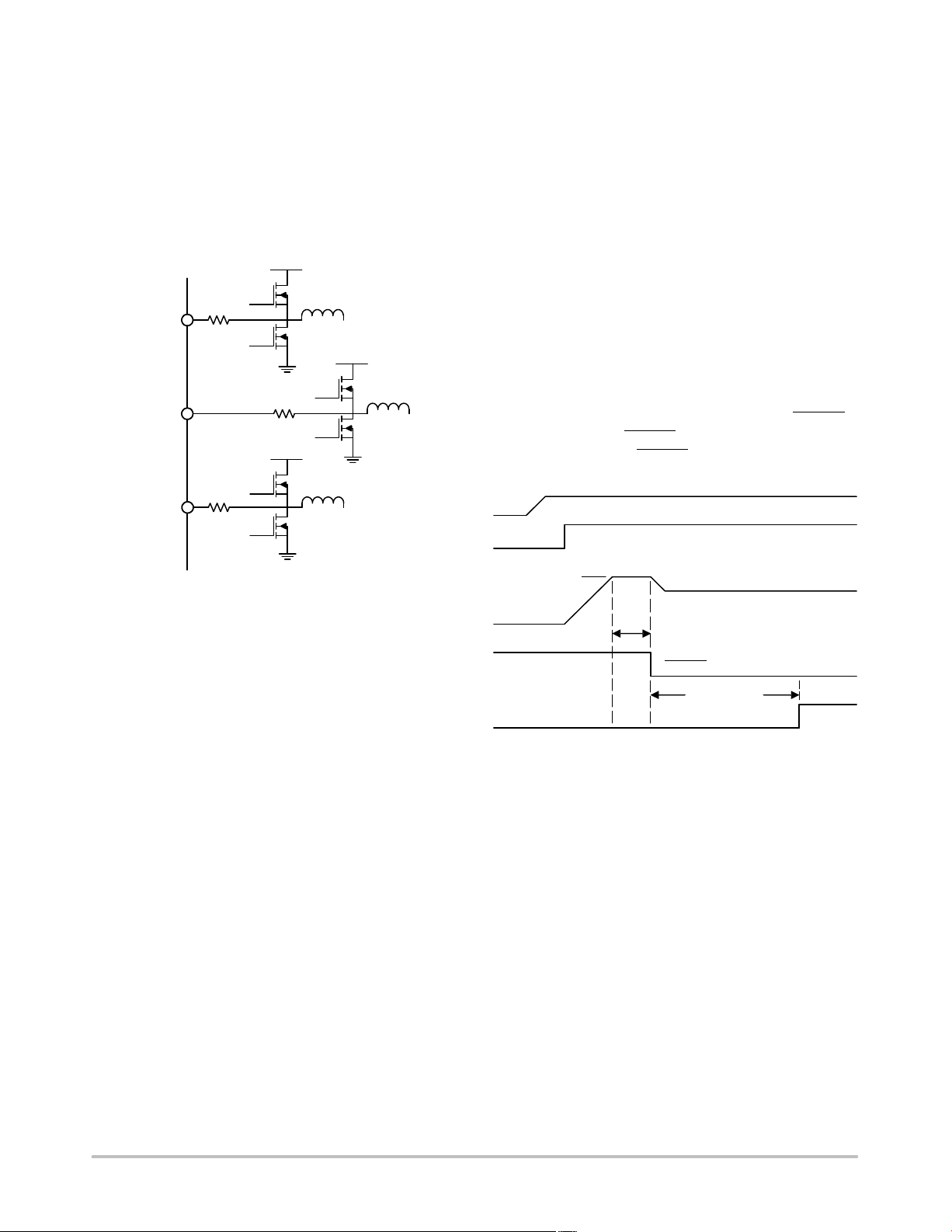
External resistors are placed in series with the SWFB1,
SWFB2, and SWFB3 pins to create an intentional current
imbalance. Such a condition can exist when one phase has
better cooling and supports higher currents the other phases.
Resistors RSWSB1, RSWFB2, and RSWFB3 (see
Figure 25) can be used to adjust thermal balance. It is
recommended to add these resistors during the initial design
to make sure placeholders are provided in the layout.
http://onsemi.com
16
Page 17
ADP3212A, NCP3218A
To increase the current in any given phase, users should
make RSWFB for that phase larger (that is, RSWFB = 100 W
for the hottest phase and do not change it during balance
optimization). Increasing RSWFB to 150 W makes a
substantial increase in phase current. Increase each RSWFB
value by small amounts to achieve thermal balance starting
with the coolest phase.
If adjusting current balance between phases is not needed,
RSWFB should be 100 W for all phases.
VDC
R
SWFB2
VDC
Phase 1
Inductor
Phase 3
Inductor
VDC
Phase 2
Inductor
ADP3212
SWFB1
SWFB2
SWFB3
R
33
28
R
24
SWFB1
SWFB3
PWRGD range is monitored. To prevent a false alarm, the
power−good circuit is masked during various system
transitions, including a VID change and entrance into or exit
out of deeper sleep. The duration of the PWRGD mask is set
to approximately 130 ms by an internal timer. If the voltage
drop is greater than 200 mV during deeper sleep entry or
slow deeper sleep exit, the duration of PWRGD masking is
extended by the internal logic circuit.
Powerup Sequence and Soft−Start
The power−on ramp−up time of the output voltage is set
internally. The APD3212A/NCP3218A steps sequentially
through each VID code until it reaches the boot voltage. The
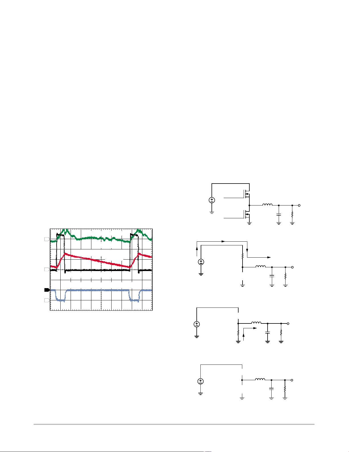
powerup sequence, including the soft−start is illustrated in
Figure 20.
After EN is asserted high, the soft−start sequence starts.
The core voltage ramps up linearly to the boot voltage. The
APD3212A/NCP3218A regulates at the boot voltage for
approximately 90 ms. After the boot time is over, CLKEN
asserted low. Before CLKEN
are ignored. 9 ms after CLKEN
is asserted low, the VID pins
is asserted low, PWRGD is
is
asserted high.
VCC = 5 V
EN
Figure 19. Current Balance Resistors
Voltage Control Mode
A high−gain bandwidth error amplifier is used for the
voltage mode control loop. The non−inverting input voltage
is set via the 7−bit VID DAC. The VID codes are listed in
Table 3. The non−inverting input voltage is offset by the
droop voltage as a function of current, commonly known as
active voltage positioning. The output of the error amplifier
is the COMP pin, which sets the termination voltage of the
internal PWM ramps.
At the negative input, the FB pin is tied to the output sense
location using R
, a resistor for sensing and controlling the
B
output voltage at the remote sensing point. The main loop
compensation is incorporated in the feedback network
connected between the FB and COMP pins.
Power−Good Monitoring
The power−good comparator monitors the output voltage
via the CSREF pin. The PWRGD pin is an open−drain
output that can be pulled up through an external resistor to
a voltage rail; not necessarily the same VCC voltage rail that
is running the controller. A logic high level indicates that the
output voltage is within the voltage limits defined by a range
around the VID voltage setting. PWRGD goes low when the
output voltage is outside of this range.
Following the IMVP−6.5 specification, the PWRGD
range is defined to be 300 mV less than and 200 mV greater
than the actual VID DAC output voltage. For any DAC
voltage less than 300 mV, only the upper limit of the
V
= 1.1 V
BOOT
V
CORE
t
BOOT
CLKEN
t
CPU_PWRGD
PWRGD
Figure 20. Powerup Sequence of
APD3212A/NCP3218A
Current Limit
The APD3212A/NCP3218A compares the differential
output of a current sense amplifier to a programmable
current limit set point to provide the current limiting
function. The current limit threshold is set by the user with
a resistor connected from the ILIM pin to CSCOMP.
Changing VID On−The−Fly (OTF)
The APD3212A/NCP3218A is designed to track
dynamically changing VID code. As a consequence, the
CPU VCC voltage can change without the need to reset the
controller or the CPU. This concept is commonly referred to
as VID OTF transient. A VID OTF can occur with either
light or heavy load conditions. The processor alerts the
controller that a VID change is occurring by changing the
VID inputs in LSB incremental steps from the start code to
the finish code. The change can be either upwards or
downwards steps.
http://onsemi.com
17
Page 18
ADP3212A, NCP3218A
When a VID input changes, the APD3212A/NCP3218A
detects the change but ignores new code for a minimum of
400 ns. This delay is required to prevent the device from
reacting to digital signal skew while the 7−bit VID input
code is in transition. Additionally, the VID change triggers
a PWRGD masking timer to prevent a PWRGD failure.
Each VID change resets and retriggers the internal PWRGD
masking timer.
As listed in Table 3, during a VID transient, the
APD3212A/NCP3218A forces PWM mode regardless of
the state of the system input signals. For example, this means
that if the chip is configured as a dual−phase controller but
is running in single−phase mode due to a light load
condition, a current overload event causes the chip to switch
to dual−phase mode to share the excessive load until the
delayed current limit latchoff cycle terminates.
In user−set single−phase mode, the
APD3212A/NCP3218A usually runs in RPM mode. When a
VID transition occurs, however, the APD3212A/NCP3218A
switches to dual−phase PWM mode.
Light Load RPM DCM Operation
In single−phase normal mode, DPRSLP is pulled low and
the APD3208 operates in Continuous Conduction Mode
(CCM) over the entire load range. The upper and lower
MOSFETs run synchronously and in complementary phase.
See Figure 21 for the typical waveforms of the
APD3212A/NCP3218A running in CCM with a 7 A load
current.
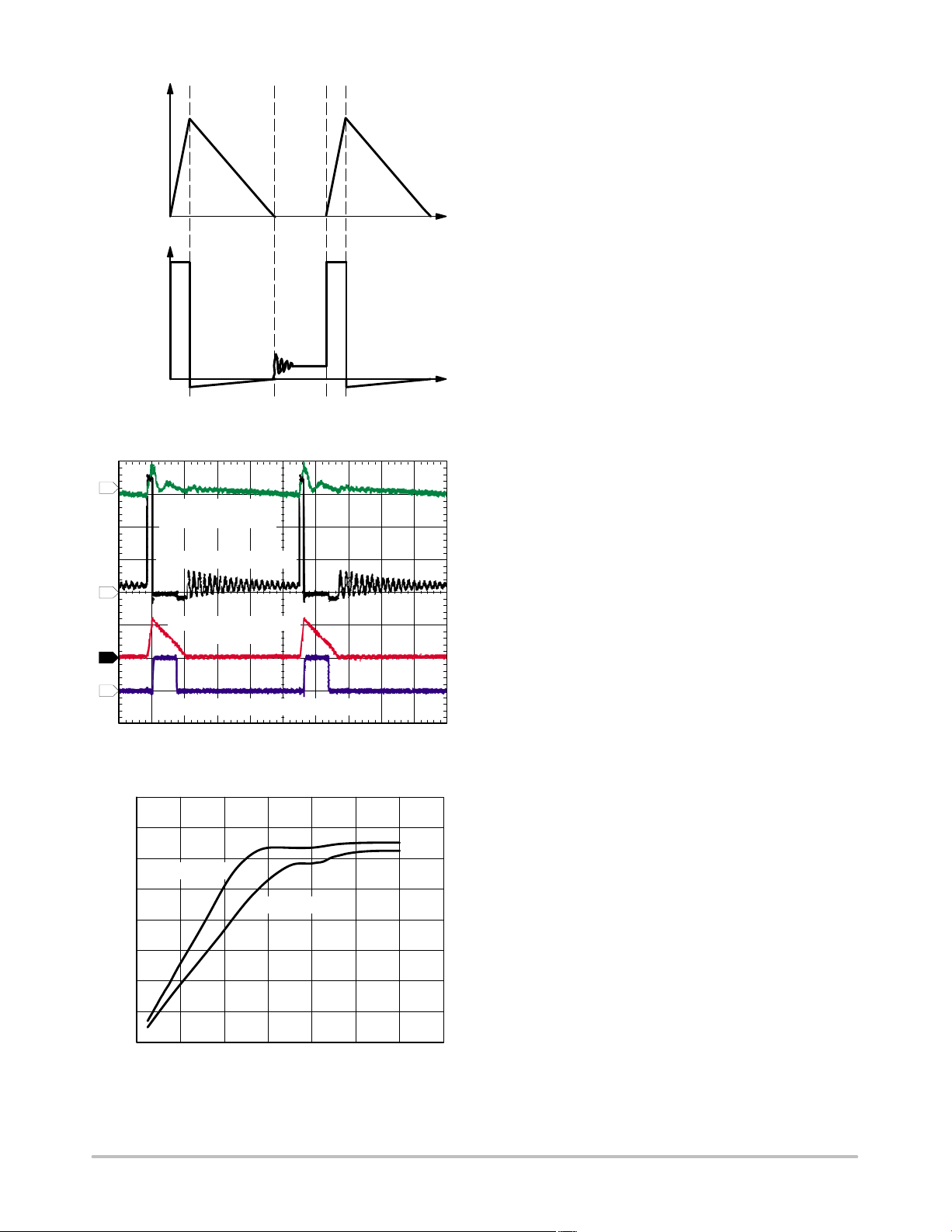
In DCM with a light load, the APD3212A/NCP3218A
monitors the switch node voltage to determine when to turn
off the low−side FET. Figure 27 shows a typical waveform in
DCM with a 1 A load current. Between t
and t2, the inductor
1
current ramps down. The current flows through the source
drain of the low−side FET and creates a voltage drop across
the FET with a slightly negative switch node. As the inductor
current ramps down to 0 A, the switch voltage approaches
0 V, as seen just before t
. When the switch voltage is
2
approximately −6 mV, the low−side FET is turned off.
Figure 26 shows a small, dampened ringing at t
. This is
2
caused by the LC created from capacitance on the switch
node, including the C
of the FETs and the output inductor.
DS
This ringing is normal.
The APD3212A/NCP3218A automatically goes into
DCM with a light load. Figure 27 shows the typical DCM
waveform of the APD3212A/NCP3218A. As the load
increases, the APD3212A/NCP3218A enters into CCM. In
DCM, frequency decreases with load current. Figure 28
shows switching frequency vs. load current for a typical
design. In DCM, switching frequency is a function of the
inductor, load current, input voltage, and output voltage.
Q1
INPUT
VOLTAGE
DRVH
DRVL
Q2
SWITCH
NODE
L
OUTPUT
VOLTAGE
C
LOAD
4
2
3
1
LOW−SIDE GATE DRIVE 5 V/DIV
Figure 21. Single−Phase Waveforms in CCM
OUTPUT VOLTAGE
20 mV/DIV
INDUCTOR CURRENT
5 A/DIV
SWITCH NODE 5 V/DIV
400 ns/DIV
If DPRSLP is pulled high, the APD3212A/NCP3218A
operates in RPM mode. If the load condition is light, the chip
enters Discontinuous Conduction Mode (DCM). Figure 22
shows a typical single−phase buck with one upper FET, one
lower FET, an output inductor, an output capacitor, and a
load resistor. Figure 23 shows the path of the inductor
current with the upper FET on and the lower FET off. In
Figure 24, the high−side FET is off and the low−side FET is
on. In CCM, if one FET is on, its complementary FET must
be off; however, in DCM, both high− and low−side FETs are
off and no current flows into the inductor (see Figure 25).
Figure 26 shows the inductor current and switch node
voltage in DCM.
Figure 22. Buck Topology
ON
L
OFF
Figure 23. Buck Topology Inductor Current
During t
OFF
ON
Figure 24. Buck Topology Inductor Current
During t
Figure 25. Buck Topology Inductor Current During
OFF
OFF
t
2
and t
0
and t
1
and t
L
L
3
C
LOAD
1
C
LOAD
2
C
LOAD
http://onsemi.com
18
Page 19
ADP3212A, NCP3218A
Output Crowbar
To prevent the CPU and other external components from
damage due to overvoltage, the APD3212A/NCP3218A
Inductor
Current
Switch
Node
Voltage
t0t
1
Figure 26. Inductor Current and Switch Node in DCM
4
OUTPUT VOLTAGE
20 mV/DIV
SWITCH NODE 5 V/DIV
2
INDUCTOR CURRENT
5 A/DIV
3
1
LOW−SIDE GATE DRIVE 5 V/DIV
Figure 27. Single−Phase Waveforms in DCM with 1 A
400
350
300
250
200
150
FREQUENCY (kHz)
100
50
Figure 28. Single−Phase CCM/DCM Frequency vs.
9 V INPUT
0
014
24681012
t
2
2 μs/DIV
Load Current
19 V INPUT
LOAD CURRENT (A)
Load Current
t3t
4
turns off the DRVH1 and DRVH2 outputs and turns on the
DRVL1 and DRVL2 outputs when the output voltage
exceeds the OVP threshold (1.55 V typical).
Turning on the low−side MOSFETs forces the output
capacitor to discharge and the current to reverse due to
current build up in the inductors. If the output overvoltage
is due to a drain−source short of the high−side MOSFET,
turning on the low−side MOSFET results in a crowbar
across the input voltage rail. The crowbar action blows the
fuse of the input rail, breaking the circuit and thus protecting
the microprocessor from destruction.
When the OVP feature is triggered, the
APD3212A/NCP3218A is latched off. The latchoff function
can be reset by removing and reapplying VCC to the
APD3212A/NCP3218A or by briefly pulling the EN pin low.
Pulling TTSNS to less than 1.0 V disables the overvoltage
protection function. In this configuration, VRTT should be
tied to ground.
Reverse Voltage Protection
Very large reverse current in inductors can cause negative
V
voltage, which is harmful to the CPU and other
CORE
output components. The APD3212A/NCP3218A provides
a Reverse Voltage Protection (RVP) function without
additional system cost. The V
through the CSREF pin. When the CSREF pin voltage drops
to less than −300 mV, the APD3212A/NCP3218A triggers
the RVP function by disabling all PWM outputs and driving
DRVL1 and DRVL2 low, thus turning off all MOSFETs. The
reverse inductor currents can be quickly reset to 0 by
discharging the built−up energy in the inductor into the input
dc voltage source via the forward−biased body diode of the
high−side MOSFETs. The RVP function is terminated when
the CSREF pin voltage returns to greater than −100 mV.
Sometimes the crowbar feature inadvertently causes
output reverse voltage because turning on the low−side
MOSFETs results in a very large reverse inductor current. To
prevent damage to the CPU caused from negative voltage,
the APD3212A/NCP3218A maintains its RVP monitoring
function even after OVP latchoff. During OVP latchoff, if
the CSREF pin voltage drops to less than −300 mV, the
low−side MOSFETs is turned off. DRVL outputs are
allowed to turn back on when the CSREF voltage recovers
to greater than −100 mV.
Output Enable and UVLO
For the APD3212A/NCP3218A to begin switching, the
VCC supply voltage to the controller must be greater than
the V
threshold and the EN pin must be driven high. If
CCOK
the VCC voltage is less than the V
EN pin is a logic low, the APD3212A/NCP3218A shuts off.
In shutdown mode, the controller holds the PWM outputs
low, shorts the capacitors of the SS and PGDELAY pins to
ground, and drives the DRVH and DRVL outputs low.
voltage is monitored
CORE
CCUVLO
threshold or the
http://onsemi.com
19
Page 20

ADP3212A, NCP3218A
The user must adhere to proper power−supply sequencing
during startup and shutdown of the APD3212A/
NCP3218A. All input pins must be at ground prior to
removing or applying VCC, and all output pins should be
left in high impedance state while VCC is off.
logic level signal at the VRTT output when the temperature
trips the user−set alarm threshold. The VRTT output is
designed to drive an external transistor that in turn provides
the high current, open−drain VRTT signal required by the
IMVP−6.5 specification. The internal VRTT comparator
has a hysteresis of approximately 100 mV to prevent high
Thermal Throttling Control
The APD3212A/NCP3218A includes a thermal
monitoring circuit to detect whether the temperature of the
VR has exceeded a user−defined thermal throttling
threshold. The thermal monitoring circuit requires an
external resistor divider connected between the VCC pin
and GND. The divider consists of an NTC thermistor and a
resistor. To generate a voltage that is proportional to
temperature, the midpoint of the divider is connected to the
TTSNS pin. An internal comparator circuit compares the
frequency oscillation of VRTT when the temperature
approaches the set alarm point.
Output Current Monitor
The APD3212A/NCP3218A has an output current
monitor. The IMON pin sources a current proportional to the
inductor current. A resistor from IMON pin to FBRTN sets
the gain. A 0.1 mF is added in parallel with R
inductor ripple. The IMON pin is clamped to prevent it from
going above 1.15 V.
TTSNS voltage to half the VCC threshold and outputs a
Table 3. VID CODE TABLE
VID6 VID5 VID4 VID3 VID2 VID1 VID0 Output (V)
0 0 0 0 0 0 0 1.5000 V
0 0 0 0 0 0 0 1.5000 V
0 0 0 0 0 0 1 1.4875 V
0 0 0 0 0 1 0 1.4750 V
0 0 0 0 0 1 1 1.4625 V
0 0 0 0 1 0 0 1.4500 V
0 0 0 0 1 0 1 1.4375 V
0 0 0 0 1 1 0 1.4250 V
0 0 0 0 1 1 1 1.4125 V
0 0 0 1 0 0 0 1.4000 V
0 0 0 1 0 0 1 1.3875 V
0 0 0 1 0 1 0 1.3750 V
0 0 0 1 0 1 1 1.3625 V
0 0 0 1 1 0 0 1.3500 V
0 0 0 1 1 0 1 1.3375 V
0 0 0 1 1 1 0 1.3250 V
0 0 0 1 1 1 1 1.3125 V
0 0 1 0 0 0 0 1.3000 V
0 0 1 0 0 0 1 1.2875 V
0 0 1 0 0 1 0 1.2750 V
0 0 1 0 0 1 1 1.2625 V
0 0 1 0 1 0 0 1.2500 V
0 0 1 0 1 0 1 1.2375 V
0 0 1 0 1 1 0 1.2250 V
0 0 1 0 1 1 1 1.2125 V
0 0 1 1 0 0 0 1.2000 V
0 0 1 1 0 0 1 1.1875 V
0 0 1 1 0 1 0 1.1750 V
0 0 1 1 0 1 1 1.1625 V
0 0 1 1 1 0 0 1.1500 V
0 0 1 1 1 0 1 1.1375 V
0 0 1 1 1 1 0 1.1250 V
0 0 1 1 1 1 1 1.1125 V
to filter the
MON
http://onsemi.com
20
Page 21

ADP3212A, NCP3218A
Table 3. VID CODE TABLE (continued)
VID6 Output (V)VID0VID1VID2VID3VID4VID5
0 1 0 0 0 0 0 1.1000 V
0 1 0 0 0 0 1 1.0875 V
0 1 0 0 0 1 0 1.0750 V
0 1 0 0 0 1 1 1.0625 V
0 1 0 0 1 0 0 1.0500 V
0 1 0 0 1 0 1 1.0375 V
0 1 0 0 1 1 0 1.0250 V
0 1 0 0 1 1 1 1.0125 V
0 1 0 1 0 0 0 1.0000 V
0 1 0 1 0 0 1 0.9875 V
0 1 0 1 0 1 0 0.9750 V
0 1 0 1 0 1 1 0.9625 V
0 1 0 1 1 0 0 0.9500 V
0 1 0 1 1 0 1 0.9375 V
0 1 0 1 1 1 0 0.9250 V
0 1 0 1 1 1 1 0.9125 V
0 1 1 0 0 0 0 0.9000 V
0 1 1 0 0 0 1 0.8875 V
0 1 1 0 0 1 0 0.8750 V
0 1 1 0 0 1 1 0.8625 V
0 1 1 0 1 0 0 0.8500 V
0 1 1 0 1 0 1 0.8375 V
0 1 1 0 1 1 0 0.8250 V
0 1 1 0 1 1 1 0.8125 V
0 1 1 1 0 0 0 0.8000 V
0 1 1 1 0 0 1 0.7875 V
0 1 1 1 0 1 0 0.7750 V
0 1 1 1 0 1 1 0.7625 V
0 1 1 1 1 0 0 0.7500 V
0 1 1 1 1 0 1 0.7375 V
0 1 1 1 1 1 0 0.7250 V
0 1 1 1 1 1 1 0.7125 V
1 0 0 0 0 0 0 0.7000 V
1 0 0 0 0 0 1 0.6875 V
1 0 0 0 0 1 0 0.6750 V
1 0 0 0 0 1 1 0.6625 V
1 0 0 0 1 0 0 0.6500 V
1 0 0 0 1 0 1 0.6375 V
1 0 0 0 1 1 0 0.6250 V
1 0 0 0 1 1 1 0.6125 V
1 0 0 1 0 0 0 0.6000 V
1 0 0 1 0 0 1 0.5875 V
1 0 0 1 0 1 0 0.5750 V
1 0 0 1 0 1 1 0.5625 V
1 0 0 1 1 0 0 0.5500 V
1 0 0 1 1 0 1 0.5375 V
1 0 0 1 1 1 0 0.5250 V
1 0 0 1 1 1 1 0.5125 V
1 0 1 0 0 0 0 0.5000 V
http://onsemi.com
21
Page 22

ADP3212A, NCP3218A
Table 3. VID CODE TABLE (continued)
VID6 Output (V)VID0VID1VID2VID3VID4VID5
1 0 1 0 0 0 1 0.4875 V
1 0 1 0 0 1 0 0.4750 V
1 0 1 0 0 1 1 0.4625 V
1 0 1 0 1 0 0 0.4500 V
1 0 1 0 1 0 1 0.4375 V
1 0 1 0 1 1 0 0.4250 V
1 0 1 0 1 1 1 0.4125 V
1 0 1 1 0 0 0 0.4000 V
1 0 1 1 0 0 1 0.3875 V
1 0 1 1 0 1 0 0.3750 V
1 0 1 1 0 1 1 0.3625 V
1 0 1 1 1 0 0 0.3500 V
1 0 1 1 1 0 1 0.3375 V
1 0 1 1 1 1 0 0.3250 V
1 0 1 1 1 1 1 0.3125 V
1 1 0 0 0 0 0 0.3000 V
1 1 0 0 0 0 1 0.2875 V
1 1 0 0 0 1 0 0.2750 V
1 1 0 0 0 1 1 0.2625 V
1 1 0 0 1 0 0 0.2500 V
1 1 0 0 1 0 1 0.2375 V
1 1 0 0 1 1 0 0.2250 V
1 1 0 0 1 1 1 0.2125 V
1 1 0 1 0 0 0 0.2000 V
1 1 0 1 0 0 1 0.1875 V
1 1 0 1 0 1 0 0.1750 V
1 1 0 1 0 1 1 0.1625 V
1 1 0 1 1 0 0 0.1500 V
1 1 0 1 1 0 1 0.1375 V
1 1 0 1 1 1 0 0.1250 V
1 1 0 1 1 1 1 0.1125 V
1 1 1 0 0 0 0 0.1000 V
1 1 1 0 0 0 1 0.0875 V
1 1 1 0 0 1 0 0.0750 V
1 1 1 0 0 1 1 0.0625 V
1 1 1 0 1 0 0 0.0500 V
1 1 1 0 1 0 1 0.0375 V
1 1 1 0 1 1 0 0.0250 V
1 1 1 0 1 1 1 0.0125 V
1 1 1 1 0 0 0 0.0000 V
1 1 1 1 0 0 1 0.0000 V
1 1 1 1 0 1 0 0.0000 V
1 1 1 1 0 1 1 0.0000 V
1 1 1 1 1 0 0 0.0000 V
1 1 1 1 1 0 1 0.0000 V
1 1 1 1 1 1 0 0.0000 V
1 1 1 1 1 1 1 0.0000 V
http://onsemi.com
22
Page 23
VSSSense
VSSSense
SHORTPIN
VCCSense
1
R50
100
VCCSense
2
2
C33 10 mF
2
C34
2
C35
2
C36
2
C37
2
C38 10 mF
2
C39
2
C40
2
C41
2
C42
2
C43
2
C44
2
C45 10 mF
2
C46
2
C47
2
JP1
C48 10 mF
2
12
C49
2
C50 10 mF
2
C51 10 mF
2
C52
2
C53 10 mF
2
C54
2
C55 10 mF
C56 10 mF
C57
C58
C59
C60
C61 10 mF
C62
C63 10 mF
C64
VCC(core) RTN
100
1
1
1
1
1
1
1
1
1
1
1
1
1
1
1
1
1
1
1
1
1
1
1
12
12
12
12
12
12
12
12
12
1
R10
VSS_S
2
VCC(core)
10 mF
10 mF
10 mF
10 mF
10 mF
10 mF
10 mF
10 mF
10 mF
10 mF
10 mF
10 mF
10 mF
10 mF
10 mF
10 mF
10 mF
10 mF
10
mF
10 mF
10 mF
C65
2
330 mF
C66
2
330 mF
C67
2
DNP
C68
2
DNP
C69
2
330 mF
C70
2
330 mF
1
J6
VCC_S
1n
C14
12
12
12
73.2 k
1 2
220kTHERMISTOR 5%
Up to 32 pieces of MLCC, X5R, 0805, 6.3 V.
4 pieces of Panasonic SP CAP (SD) or Sanyo POSCAP.
1
1
1
1
1
1
1
J5
CSREF
J7
CON2
1 2
12
12
R19
C12
150p
C13
1
1.5n
165 k
R21
2
R22
R23
Place R23 close to
output inductor of
phase 1.
VCC
ADP3611
U13
DRVL
3
2
1
Q22
NTMFS4821N
C79
2
1
DNP
D9
DNP
0.45 mH/ESR =
1.1 mW
PH3_CS+
1
Note 2
2
CSREF
R20
12
DNP
12
0
R52
R63
R51 DNP
1
1
DNP
DNP
2
2
PH3_CS+
54321
CROWBAR
DRVLSD
SD
DRVH
GND
SW
6
8
7
9
4
5
6
7
8
3
2
1
Q20
NTMFS4821N
R57
1
2
C
DNP
12
SW3
SW3
1
L3
2
R64 10
RS3 DNP
1
1
JP4
2
DNP
R65
1
2
VCORE
2
Note 3
VDC
12
R18
0
1n
12
C11
R26
R25 115 k
1
1
1
115 k
2
2
2
IN
4.7 mF/
BST
16 V
X5R
(1206)
10
C14
12
R42
12
0
C78
12
0.47 m
4
5
6
7
8
C103
12
1n
1
C21
J26
12
10 mF
C30
12
10 mF
C31
12
PH3 VCORE cut
10 mF
C32
1
2
10 mF
ADP3212A, NCP3218A
1
1
VRTT
9
TRDET
VRTT10TTSNS
VARFREQ
ADP3212A
SWFB2
DRVL2
SW2
27
28
12
R62
0
4
Q9
C29
12
B
DNP
12
DNPD8
1
J9
R54
10
12
Note 2
12
R31
DNP
VCORE
1
2
1
2
12
8
COMP
LFCSP48
PGND
29
3
2
1
CSREF
DNP
R24
115 k
V5S
V5S
12
R73
12
0
R74
R27
2
80.6 k
R15
2
280 k
R16
2
402 k
R17
280 k
R14
2
4.53 k
1
2
NTMFS4821N
Q8
VDC
J3
COMP
J2
TRDET
1
1
13
IREF
14
RPM
1
15
RT
12
16
RAMP
17
LLINE
18
CSREF
19
CSSUM
20
CSCOMP
21
1
ILIM
22
OD3
23
PWM3
24
SWFB3
1 2
R66
0
SW3
R33
12
C22
12
0.47 m
5
6
7
8
Q7
NTMFS4821N
C102
1
2
1n
C23
1
2
10 mF
C24
1
2
10 mF
C25
1
2
10 mF
C26
1
2
10 mF
VDC
PH2 VCORE cut
1
1
R68
2
C104
69.8 k
12
R67
2
860 pF
4.99 k
TTSense
11
12
GND
DRVH2
BST2
26
25
0
5
6
7
4
8
3
2
1
NTMFS4846N
R56
12
DNP
SW2
1
NEC Tokin MPCG10LR45
L2
0.45 mH/ESR = 1.1 mW
2
(Optional)
1
RS2 DNP
12
JP3
2
R12
R13
12p
1.65 k
C7
C8
7
30
1
2
390 pF
39.2 k
12
6
FB
DRVL1
31
C15
C6
330p
5
FBRTN
PVCC
32
R61
12
CSREF
1
R11
0
2
1
2
C5
1n
3
4
IMON
CLKEN
SWFB1
SW1
34
33
12
0
4.7 mF
3
2
1
NTMFS4846N
C28
2
DNP
D5
R53
10
Note 2
12
R30
DNP
CLKEN#
VR_ON
2
EN
PWRGD
DPRSLP
DRVH1
BST1
35
4
Q4
R55
1
A
DNP
12
DNP
SW1
12
R45
12
1
3 k
PWRGD
J22
3 k
1
2
PWRGD
1
R46
J23
R60
1
IMON
0.1 m
7.50 k
2
C4
2
1
1
U1
48
VID0
47
VID1
46
VID2
45
VID3
44
VID4
43
VID5
42
VID6
41
PSI
40
39
PH0
38
PH1
37
VCC
C3
2
36
1 mF/16 V
X7R(0805)
R32
0
0.47 m
5
6
7
4
8
3
2
1
C101
2
2
12
10 mF
2
10 mF
1
(Optional)
10 mF
J8
10 mF
1
NEC Tokin MPCG10LR45
L1
0.45 mH/ESR = 1.1 mW
2
RS1 DNP
12
12
JP2
Thermistor R4 should be
placed close to the hot
spot of the board.
V3.3S
1
J24
VID0
VID1
VID2
VID3
VID4
VID5
VID6
2
PSI
DPRSLPVR
2
1
R8
10
1
V5S
12
12
C16
5
6
Q2
7
NTMFS4821N
8
1
1n
1
C17
1
C18
12
C19
12
VDC
C20
PH1 VCORE cut
IMVP−6.5 solution for Penryn
processor: 3−phase/55−65 A
DNP
R70
DNP
R72
R4
100 k
Therm..
5%
12
1
12
C1
10n
X7R
R69
R71
12
0
0
R1
7.32 k
TTSense
12
12
12
V5S
Figure 29. Typical Dual−Phase Application Circuit
http://onsemi.com
23
Page 24

ADP3212A, NCP3218A
Application Information
The design parameters for a typical IMVP−6.5−compliant
CPU core VR application are as follows:
• Maximum input voltage (V
• Minimum input voltage (V
• Output voltage by VID setting (V
• Maximum output current (I
• Droop resistance (R
) = 1.9 mW
O
• Nominal output voltage at 40 A load (V
INMAX
INMIN
) = 52 A
O
) = 19 V
) = 8.0 V
) = 1.05 V
VID
OFL
) = 0.9512 V
• Static output voltage drop from no load to full load
(DV) = V
• Maximum output current step (DI
ONL
− V
= 1.05 V − 0.9512 V = 98 mV
OFL
) = 52 A
O
• Number of phases (n) = 2
• Switching frequency per phase (ƒ
• Duty cycle at maximum input voltage (D
• Duty cycle at minimum input voltage (D
Setting the Clock Frequency for PWM
In PWM operation, the APD3212A/NCP3218A uses a
fixed−frequency control architecture. The frequency is set
by an external timing resistor (RT). The clock frequency and
the number of phases determine the switching frequency per
phase, which relates directly to the switching losses and the
sizes of the inductors and input and output capacitors. For a
dual−phase design, a clock frequency of 600 kHz sets the
switching frequency to 300 kHz per phase. This selection
represents the trade−off between the switching losses and
the minimum sizes of the output filter components. To
achieve a 600 kHz oscillator frequency at a VID voltage of
1.2 V, RT must be 181 kW. Alternatively, the value for RT
can be calculated by using the following equation:
V
) 1.0 V
RT+
where:
9 pF and 16 kW are internal IC component values.
V
is the VID voltage in volts.
VID
n is the number of phases.
ƒ
is the switching frequency in hertz for each phase.
SW
For good initial accuracy and frequency stability, it is
recommended to use a 1% resistor.
When VARFREQ pin is connected to ground, the
switching frequency does not change with VID. The value
for RT can be calculated by using the following equation.
RT+
Setting the Switching Frequency for
RPM Operation of Phase 1
During the RPM operation of Phase 1, the
APD3212A/NCP3218A runs in pseudoconstant frequency
if the load current is high enough for continuous current
mode. While in DCM, the switching frequency is reduced
with the load current in a linear manner.
VID
2 n f
1.0 V
n 2 f
SW
SW
9pF
9pF
) = 300 kHz
SW
* 16 kW
* 16 kW
) = 0.13 V
MAX
) = 0.055 V
MIN
(eq. 1)
(eq. 2)
To save power with light loads, lower switching frequency
is usually preferred during RPM operation. However, the
V
ripple specification of IMVP−6.5 sets a limitation
CORE
for the lowest switching frequency. Therefore, depending on
the inductor and output capacitors, the switching frequency
in RPM can be equal to, greater than, or less than its
counterpart in PWM.
A resistor from RPM to GND sets the pseudo constant
frequency as following:
R
RPM
+
V
2 R
VID
) 1.0 V
AR (1 * D) V
T
RR CR f
SW
VID
* 0.5 kW
(eq. 3)
where:
is the internal ramp amplifier gain.
A
R
C
is the internal ramp capacitor value.
R
R
is an external resistor on the RAMPADJ pin to set the
R
internal ramp magnitude.
Soft−Start and Current Limit Latchoff Delay Times
Inductor Selection
The choice of inductance determines the ripple current of
the inductor. Less inductance results in more ripple current,
which increases the output ripple voltage and the conduction
losses in the MOSFETs. However, this allows the use of
smaller−size inductors, and for a specified peak−to−peak
transient deviation, it allows less total output capacitance.
Conversely, a higher inductance results in lower ripple
current and reduced conduction losses, but it requires
larger−size inductors and more output capacitance for the
same peak−to−peak transient deviation. For a multi−phase
converter, the practical value for peak−to−peak inductor
ripple current is less than 50% of the maximum dc current
of that inductor. Equation 4 shows the relationship between
the inductance, oscillator frequency, and peak−to−peak
ripple current. Equation 5 can be used to determine the
minimum inductance based on a given output ripple voltage.
V
IR+
L w
(1 * D
VID
f
L
SW
V
RO ǒ1 * (n D
VID
fSW V
MIN
RIPPLE
)
Ǔ
)
MIN
(eq. 4)
(eq. 5)
Solving Equation 5 for a 16 mV peak−to−peak output
ripple voltage yields:
1.05 V 1.9 mW (1 * 2 0.055)
L w
300 kHz 16 mV
+ 528 nH
If the resultant ripple voltage is less than the initially
selected value, the inductor can be changed to a smaller
value until the ripple value is met. This iteration allows
optimal transient response and minimum output decoupling.
The smallest possible inductor should be used to minimize
the number of output capacitors. Choosing a 490 nH
inductor is a good choice for a starting point, and it provides
a calculated ripple current of 9.0 A. The inductor should not
saturate at the peak current of 24.5 A, and it should be able
to handle the sum of the power dissipation caused by the
http://onsemi.com
24
Page 25
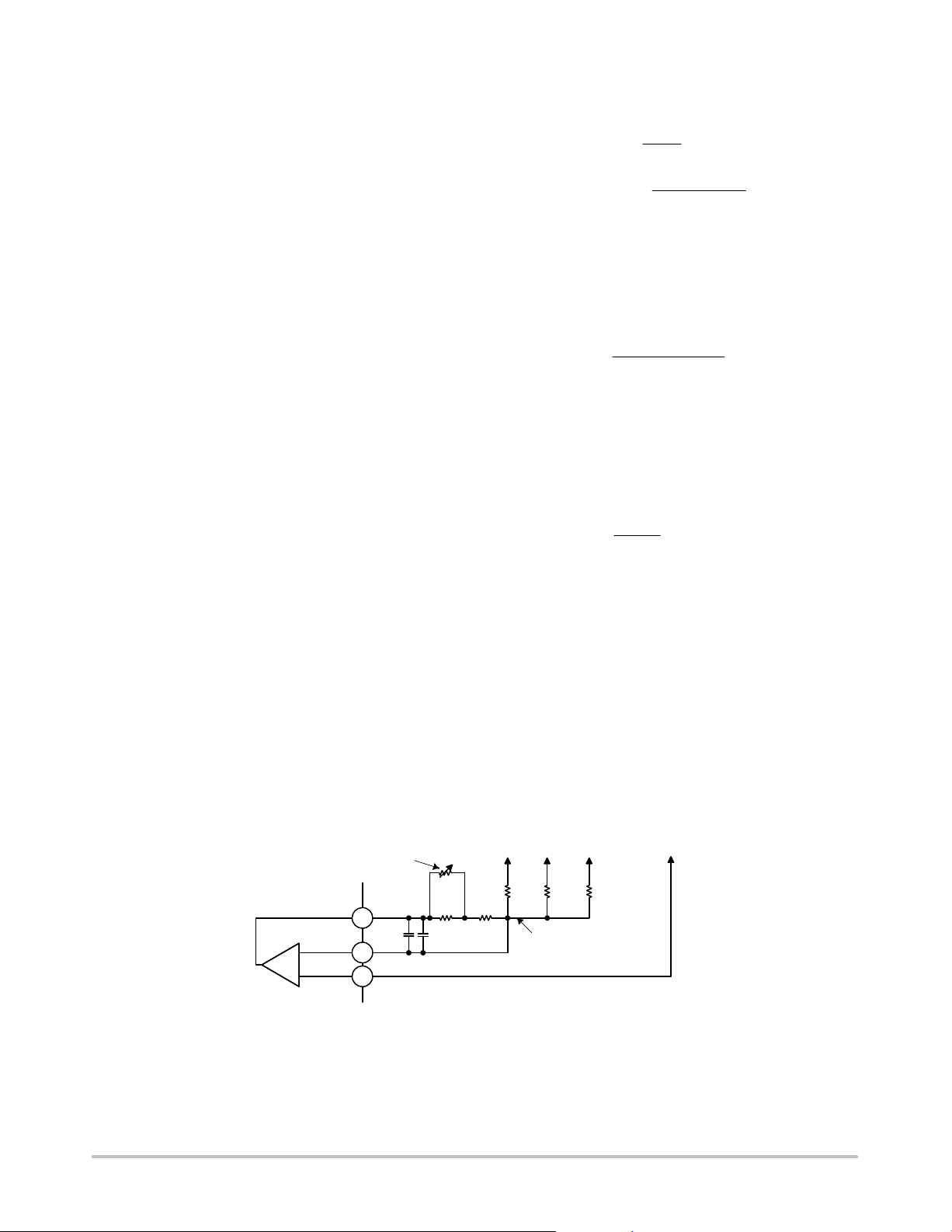
ADP3212A, NCP3218A
winding’s average current (20 A) plus the ac core loss. In this
example, 330 nH is used.
Another important factor in the inductor design is the
DCR, which is used for measuring the phase currents. Too
large of a DCR causes excessive power losses, whereas too
small of a value leads to increased measurement error. For
this example, an inductor with a DCR of 0.8 mW is used.
Selecting a Standard Inductor
After the inductance and DCR are known, select a
standard inductor that best meets the overall design goals. It
is also important to specify the inductance and DCR
tolerance to maintain the accuracy of the system. Using 20%
tolerance for the inductance and 15% for the DCR at room
temperature are reasonable values that most manufacturers
can meet.
Power Inductor Manufacturers
The following companies provide surface−mount power
inductors optimized for high power applications upon
request:
• Vishay Dale Electronics, Inc.
(605) 665−9301
• Panasonic
(714) 373−7334
• Sumida Electric Company
(847) 545−6700
• NEC Tokin Corporation
(510) 324−4110
Output Droop Resistance
The design requires that the regulator output voltage
measured at the CPU pins decreases when the output current
increases. The specified voltage drop corresponds to the
droop resistance (R
The output current is measured by summing the currents
of the resistors monitoring the voltage across each inductor
and by passing the signal through a low−pass filter. The
summing is implemented by the CS amplifier that is
configured with resistor R
).
O
(summer) and resistors R
PH(x)
CS
and CCS (filters). The output resistance of the regulator is set
by the following equations:
R
RO+
CCS+
where R
Either R
CS
is the DCR of the output inductors.
SENSE
or R
PH(x)
Due to the current drive ability of the CSCOMP pin, the R
CS
R
PH(x)
R
SENSE
R
L
SENSE
R
CS
(eq. 6)
(eq. 7)
can be chosen for added flexibility.
CS
resistance should be greater than 100 kW. For example,
initially select R
Equation 7 to solve for C
CCS+
to be equal to 200 kW, and then use
CS
:
CS
330 nH
0.8 mW 200 kW
+ 2.1 nF
If CCS is not a standard capacitance, RCS can be tuned. For
example, if the optimal C
capacitance is 1.5 nF, adjust R
CS
CS
to 280 kW. For best accuracy, CCS should be a 5% NPO
capacitor. In this example, a 220 kW is used for R
CS
to
achieve optimal results.
Next, solve for R
by rearranging Equation 6 as
PH(x)
follows:
w
0.8 mW
2.1 mW
220 kW + 83.8 kW
is 86.6 kW.
PH(x)
R
PH(x)
The standard 1% resistor for R
Inductor DCR Temperature Correction
If the DCR of the inductor is used as a sense element and
copper wire is the source of the DCR, the temperature
changes associated with the inductor’s winding must be
compensated for. Fortunately, copper has a well−known
Temperature Coefficient (TC) of 0.39%/°C.
If R
is designed to have an opposite but equal
CS
percentage of change in resistance, it cancels the
temperature variation of the inductor’s DCR. Due to the
nonlinear nature of NTC thermistors, series resistors R
and R
(see Figure 30) are needed to linearize the NTC and
CS2
CS1
produce the desired temperature coefficient tracking.
Place as close as possible
to nearest inductor
ADP3212
CSCOMP
CSSUM
−
CSREF
+
Figure 30. Temperature−Compensation Circuit Values
19
18
17
C
CS2
R
TH
R
CS1
C
CS1
http://onsemi.com
To Switch Nodes
R
R
25
PH1
CS2
Keep This Path As Short
As Possible And Well Away
From Switch Node Lines
To V
Sense
OUT
R
R
PH2
PH3
Page 26

ADP3212A, NCP3218A
The following procedure and expressions yield values for
R
, R
CS1
given R
, and RTH (the thermistor value at 25°C) for a
CS2
value.
CS
1. Select an NTC to be used based on its type and
value. Because the value needed is not yet
determined, start with a thermistor with a value
close to R
and an NTC with an initial tolerance
CS
of better than 5%.
2. Find the relative resistance value of the NTC at
two temperatures. The appropriate temperatures
will depend on the type of NTC, but 50°C and
90°C have been shown to work well for most types
of NTCs. The resistance values are called A (A is
R
(50°C)/RTH(25°C)) and B (B is
TH
R
(90°C)/RTH(25°C)). Note that the relative
TH
value of the NTC is always 1 at 25°C.
3. Find the relative value of R
required for each of
CS
the two temperatures. The relative value of R
based on the percentage of change needed, which
is initially assumed to be 0.39%/°C in this
example.
The relative values are called r
(T
− 25))) and r2 (r2 is 1/(1 + TC × (T2 − 25))),
1
where TC is 0.0039, T
is 50°C, and T2 is 90°C.
1
4. Compute the relative values for r
(r1 is 1/(1+ TC ×
1
, r
CS2
, and r
CS1
by using the following equations:
r
(A−B) r1 r2* A (1−B) r2) B (1−A) r
+
CS2
A (1 * B) r1* B (1 * A) r2* (A * B)
1*r
1*r
1
1
CS2
(1 * A)
*
CS2
1
*
r
r
1
1
CS1
*r
A
CS2
r
CS1
rTH+
+
(eq. 8)
5. Calculate RTH = rTH × RCS, and then select a
thermistor of the closest value available. In
addition, compute a scaling factor k based on the
ratio of the actual thermistor value used relative to
the computed one:
R
k +
R
TH(ACTUAL)
TH(CALCULATED)
(eq. 9)
CS
6. Calculate values for R
CS1
and R
by using the
CS2
following equations:
R
+ RCS k r
CS1
R
+ RCS ǒ(1 * k) ) (k r
CS2
CS1
CS2
(eq. 10)
Ǔ
)
For example, if a thermistor value of 100 kW is selected
in Step 1, an available 0603−size thermistor with a value
close to R
is the Vishay NTHS0603N04 NTC thermistor,
CS
which has resistance values of A = 0.3359 and B = 0.0771.
Using the equations in Step 4, r
and r
is 1.094. Solving for rTH yields 241 kW, so a
TH
is 0.359, r
CS1
is 0.729,
CS2
thermistor of 220 kW would be a reasonable selection,
making k equal to 0.913. Finally, R
CS1
and R
are found
CS2
to be 72.1 kW and 166 kW. Choosing the closest 1% resistor
yields 165 kW. To correct for this approximation,
CS2
.
CS1
Selection
OUT
is
for R
73.3 kW is used for R
C
The required output decoupling for processors and
platforms is typically recommended by Intel. For systems
containing both bulk and ceramic capacitors, however, the
following guidelines can be a helpful supplement.
Select the number of ceramics and determine the total
ceramic capacitance (C
TH
1
type of capacitors used. Keep in mind that the best location
to place ceramic capacitors is inside the socket; however, the
physical limit is twenty 0805−size pieces inside the socket.
Additional ceramic capacitors can be placed along the outer
). This is based on the number and
Z
edge of the socket. A combined ceramic capacitor value of
200 mF to 300 mF is recommended and is usually composed
of multiple 10 mF or 22 mF capacitors.
Ensure that the total amount of bulk capacitance (C
) is
X
within its limits. The upper limit is dependent on the VID
OTF output voltage stepping (voltage step, V
with error of V
); the lower limit is based on meeting the
ERR
, in time, tV,
V
critical capacitance for load release at a given maximum load
step, DI
specification allows a maximum V
(V
OSMAX
. The current version of the IMVP−6.5
O
overshoot
CORE
) of 10 mV more than the VID voltage for a
step−off load current.
C
X(MIN)
ȡ
ȧ
w
ȧ
n ǒRO)
Ȣ
L DI
V
OSMAX
DI
O
Ǔ
V
O
VID
* C
ȣ
ȧ
Z
ȧ
Ȥ
(eq. 11)
C
X(MAX)
v
L
2
R
n k
http://onsemi.com
V
2
V
VID
O
where k + − ln
26
ȡ
V
Ǹ
ȧ
1 )ǒt
V
v
Ȣ
V
ERR
ǒ
Ǔ
V
V
VID
V
V
n k R
L
2
O
ȣ
Ǔ
* 1
* C
ȧ
Z
Ȥ
(eq. 12)
Page 27

ADP3212A, NCP3218A
To meet the conditions of these expressions and the
transient response, the ESR of the bulk capacitor bank (R
should be less than two times the droop resistance, R
C
the VID OTF and/or the deeper sleep exit specifications and
may require less inductance or more phases. In addition, the
switching frequency may have to be increased to maintain
the output ripple.
capacitors (CZ = 300 mF) are used, the fastest VID voltage
change is when the device exits deeper sleep, during which
the V
10 mV. If k = 3.1, solving for the bulk capacitance yields
C
C
ǒ
+ 21 mF
ESR of 7 mW each yields C
enough to limit the high frequency ringing during a load
change. This is tested using:
Q is limited to the square root of 2 to ensure a critically
damped system.
L
enough to avoid ringing during a load change. If the L
the chosen bulk capacitor bank is too large, the number of
ceramic capacitors may need to be increased to prevent
excessive ringing.
capacitor design can be used if the conditions of
Equations 11, 12, and 13 are satisfied.
Power MOSFETs
power MOSFETs are selected for two high−side switches
and two or three low−side switches per phase. The main
selection parameters for the power MOSFETs are V
Q
gate driver is 5.0 V, logic−level threshold MOSFETs must be
used.
requirement for the low−side (synchronous) MOSFETs. In
is greater than C
X(MIN)
For example, if 30 pieces of 10 mF, 0805−size MLC
change is 220 mV in 22 ms with a setting error of
CORE
w
X(MIN)
ȡ
ȧ
2
Ȣ
X(MAX)
Ǹ
1 )
Using six 330 mF Panasonic SP capacitors with a typical
Ensure that the ESL of the bulk capacitors (L
LXv CZ R
LXv 300 mF (2.1 mW)2 2 + 2nH
where:
is about 150 pH for the six SP capacitors, which is low
X
For this multimode control technique, an all ceramic
For typical 20 A per phase applications, the N−channel
, C
G
ISS
The maximum output current, IO, determines the R
330 nH 27.9 A
ǒ
2.1 mW )
v
2 3.1
22ms 1.4375V 2 3.1 2.1mW
ǒ
, C
RSS
10 mV
27.9 A
330 nH 220 mV
2
(2.1 mW)2 1.4375 V
220 mV 490 nH
2
Q
O
, and R
DS(ON)
, the system does not meet
X(MAX)
ȣ
* 300 mF
Ǔ
1.4375 V
= 1.98 mF and RX = 1.2 mW.
X
2
. Because the voltage of the
2
Ǔ
ȧ
Ȥ
−1Ǔ−300 mF
. If the
O
+ 1.0 mF
) is low
X
(eq. 13)
of
X
GS(TH)
DS(ON)
X
the APD3212A/NCP3218A, currents are balanced between
phases; the current in each low−side MOSFET is the output
)
current divided by the total number of MOSFETs (n
With conduction losses being dominant, the following
expression shows the total power that is dissipated in each
synchronous MOSFET in terms of the ripple current per
phase (I
PSF+ (1−D)
D is the duty cycle and is approximately the output voltage
divided by the input voltage.
I
R
approximately
allowed power dissipation, the user can calculate the
required R
8−lead SOIC compatible MOSFETs, the junction−to−
ambient (PCB) thermal impedance is 50°C/W. In the worst
case, the PCB temperature is 70°C to 80°C during heavy
load operation of the notebook, and a safe limit for P
about 0.8 W to 1.0 W at 120°C junction temperature.
Therefore, for this example (40 A maximum), the R
MOSFET is less than 8.5 mW for two pieces of low−side
MOSFETs. This R
about 120°C; therefore, the R
less than 6 mW at room temperature, or 8.5 mW at high
temperature.
is the input capacitance and feedback capacitance. The ratio
of the feedback to input must be small (less than 10% is
recommended) to prevent accidentally turning on the
synchronous MOSFETs when the switch node goes high.
two main power dissipation components: conduction losses
and switching losses. Switching loss is related to the time for
the main MOSFET to turn on and off and to the current and
voltage that are being switched. Basing the switching speed
on the rise and fall times of the gate driver impedance and
MOSFET input capacitance, the following expression
provides an approximate value for the switching loss per
main MOSFET:
,
nMF is the total number of main MOSFETs.
R
C
) and the average total output current (IO):
R
2
I
O
ǒ
Ǔ
ƪ
where:
is the inductor peak−to−peak ripple current and is
IR+
Knowing the maximum output current and the maximum
for the MOSFET. For 8−lead SOIC or
DS(ON)
DS(SF)
Another important factor for the synchronous MOSFET
The high−side (main) MOSFET must be able to handle
P
+ 2 fSW
S(MF)
where:
is the total gate resistance.
G
is the input capacitance of the main MOSFET.
ISS
)
n
SF
(1 * D) V
L f
is also at a junction temperature of
DS(SF)
VDC I
n
MF
n I
12
1
SW
O
R
ǒ
per MOSFET should be
RG
OUT
Ǔ
n
SF
).
SF
2
R
ƫ
DS(SF)
(eq. 14)
is
SF
per
DS(SF)
n
MF
C
ISS
n
(eq. 15)
http://onsemi.com
27
Page 28

ADP3212A, NCP3218A
The most effective way to reduce switching loss is to use
lower gate capacitance devices.
The conduction loss of the main MOSFET is given by the
following equation:
2
P
C(MF)
+ D
where R
I
O
ǒ
Ǔ
ƪ
DS(MF)
)
n
MF
is the on resistance of the MOSFET.
12
n I
1
ǒ
Typically, a user wants the highest speed (low C
2
R
Ǔ
R
ƫ
n
MF
DS(MF)
(eq. 16)
ISS
device for a main MOSFET, but such a device usually has
higher on resistance. Therefore, the user must select a device
that meets the total power dissipation (about 0.8 W to 1.0 W
for an 8−lead SOIC) when combining the switching and
conduction losses.
For example, an IRF7821 device can be selected as the
main MOSFET (four in total; that is, n
= 4), with
MF
approximately
= 1010 pF (maximum) and R
C
ISS
(maximum at T
= 120°C), and an IR7832 device can be
J
DS(MF)
= 18 mW
selected as the synchronous MOSFET (four in total; that is,
n
= 4), with
SF
R
power dissipation per MOSFET at I
= 6.7 mW (maximum at TJ = 120°C). Solving for the
DS(SF)
= 40 A and IR = 9.0 A
O
yields 630 mW for each synchronous MOSFET and
590 mW for each main MOSFET. A third synchronous
MOSFET is an option to further increase the conversion
efficiency and reduce thermal stress.
Finally, consider the power dissipation in the driver for
each phase. This is best described in terms of the Q
for the
G
MOSFETs and is given by the following equation:
f
SW
ƪ
P
+
DRV
where Q
(nMF Q
2 n
is the total gate charge for each main
GMF
MOSFET, and Q
) nSF Q
GMF
is the total gate charge for each
GSF
GSF
) ) I
CC
ƫ
VCC
(eq. 17)
synchronous MOSFET.
The previous equation also shows the standby dissipation
(I
times the VCC) of the driver.
CC
Ramp Resistor Selection
The ramp resistor (RR) is used to set the size of the internal
PWM ramp. The value of this resistor is chosen to provide
the best combination of thermal balance, stability, and
transient response. Use the following expression to
determine a starting value:
A
L
RR+
3 A
RR+
3 5 5.2 mW 5pF
R
RDS C
D
0.5 360 nH
R
(eq. 18)
+ 462 kW
where:
A
is the internal ramp amplifier gain.
R
A
is the current balancing amplifier gain.
D
is the total low−side MOSFET on resistance.
R
DS
C
is the internal ramp capacitor value.
R
Another consideration in the selection of R
the internal ramp voltage (see Equation 19). For stability and
noise immunity, keep the ramp size larger than 0.5 V. Taking
this into consideration, the value of R
in this example is
R
selected as 280 kW.
The internal ramp voltage magnitude can be calculated as
follows:
A
(1 * D) V
)
VR+
VR+
R
RR CR f
0.5 (1 * 0.061) 1.150 V
462 kW 5pF 280 kHz
VID
SW
+ 0.83 V
The size of the internal ramp can be increased or
decreased. If it is increased, stability and transient response
improves but thermal balance degrades. Conversely, if the
ramp size is decreased, thermal balance improves but
stability and transient response degrade. In the denominator
of Equation 18, the factor of 3 sets the minimum ramp size
that produces an optimal combination of good stability,
transient response, and thermal balance.
Current Limit Setpoint
To select the current limit setpoint, the resistor value for
R
must be determined. The current limit threshold for
CLIM
the APD3212A/NCP3218A is set with R
CLIM
found using the following equation:
I
R
LIM
+
LIM
R
O
60 mA
where:
R
is the current limit resistor.
LIM
R
is the output load line.
O
I
is the current limit setpoint.
LIM
When the APD3212A/NCP3218A is configured for 3
phase operation, the equation above is used to set the current
limit. When the APD3212A/NCP3218A switches from 3
phase to 1 phase operation by PSI
or DPRSLP signal, the
current is single phase is one third of the current limit in 3
phase.
When the APD3212A/NCP3218A is configured for 2
phase operation, the equation above is used to set the current
limit. When the APD3212A/NCP3218A switches from 2
phase to 1 phase operation by PSI
or DPRSLP signal, the
current is single phase is one half of the current limit in 2
phase.
When the APD3212A/NCP3218A is configured for 1
phase operation, the equation above is used to set the current
limit.
Current Monitor
The APD3212A/NCP3218A has output current monitor.
The IMON pin sources a current proportional to the total
inductor current. A resistor, R
, from IMON to FBRTN
MON
sets the gain of the output current monitor. A 0.1 mF is placed
in parallel with R
to filter the inductor current ripple and
MON
is the size of
R
(eq. 19)
. R
CLIM
can be
(eq. 20)
http://onsemi.com
28
Page 29
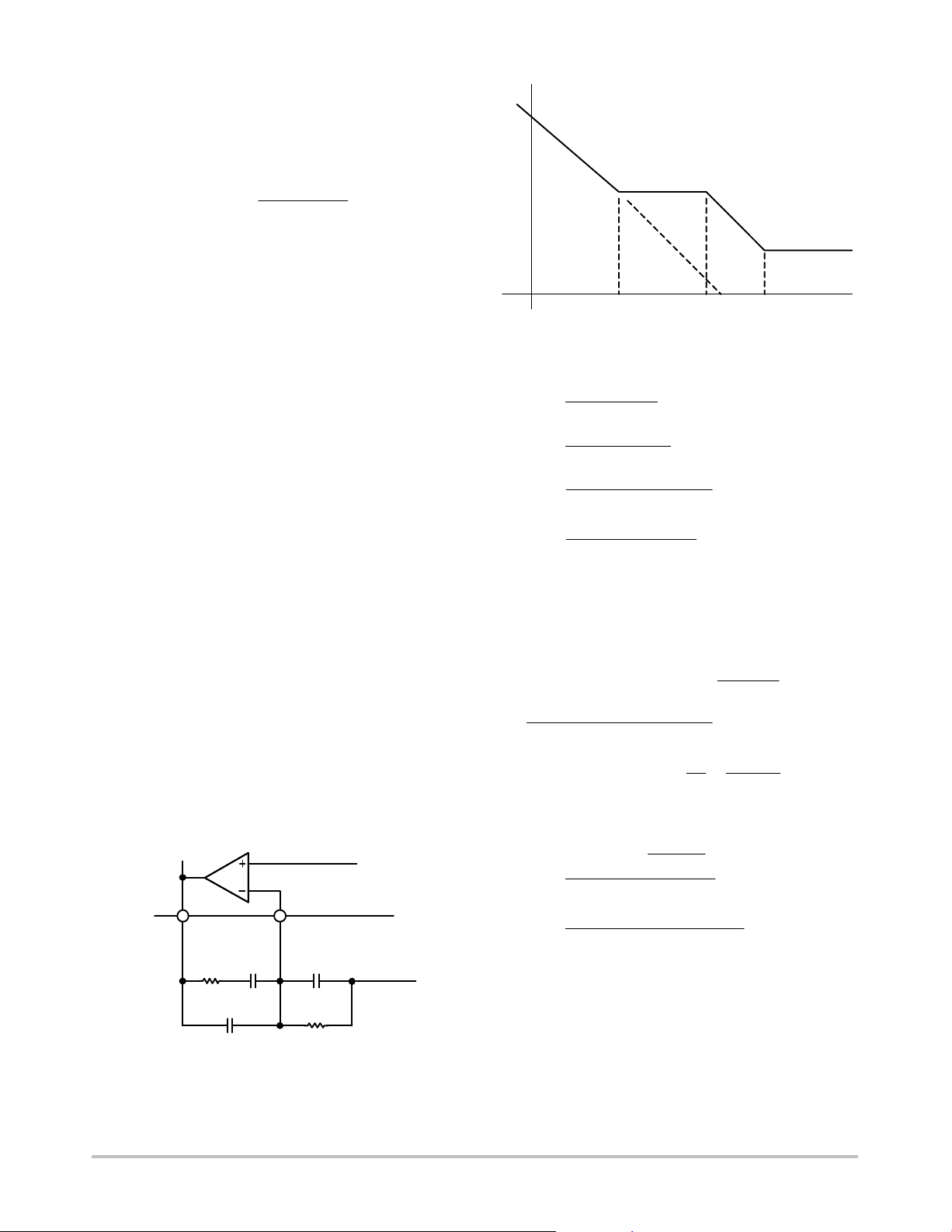
ADP3212A, NCP3218A
high frequency load transients. Since the IMON pin is
connected directly to the CPU, it is clamped to prevent it
from going above 1.15 V.
The IMON pin current is equal to the R
gain of 4. R
can be found using the following equation:
MON
MON
1.15 V R
+
4 RO I
R
LIM
LIM
FS
times a fixed
(eq. 21)
where:
is the current monitor resistor. R
R
MON
is connected
MON
from IMON pin to FBRTN.
R
is the current limit resistor.
LIM
R
is the output load line resistance.
O
I
is the output current when the voltage on IMON is at full
FS
scale.
Feedback Loop Compensation Design
Optimized compensation of the APD3212A/NCP3218A
allows the best possible response of the regulator’s output to
a load change. The basis for determining the optimum
compensation is to make the regulator and output
decoupling appear as an output impedance that is entirely
resistive over the widest possible frequency range, including
dc, and that is equal to the droop resistance (R
). With the
O
resistive output impedance, the output voltage droops in
proportion with the load current at any load current slew
rate, ensuring the optimal position and allowing the
minimization of the output decoupling.
With the multimode feedback structure of the
APD3212A/NCP3218A, it is necessary to set the feedback
compensation so that the converter’s output impedance
works in parallel with the output decoupling. In addition, it
is necessary to compensate for the several poles and zeros
created by the output inductor and decoupling capacitors
(output filter).
A Type III compensator on the voltage feedback is
adequate for proper compensation of the output filter.
Figure 31 shows the Type III amplifier used in the
APD3212A/NCP3218A. Figure 32 shows the locations of
the two poles and two zeros created by this amplifier.
VOLTAGE ERROR
AMPLIFIER
COMP
Figure 31. Voltage Error Amplifier
FB
C
R
A
A
C
B
REFERENCE
VOLTAGE
ADP3212
C
FB
R
FB
OUTPUT
VOLTAGE
Gain
−20 dB/dec
−20 dB/dec
0 dB
f
f
Z1
P0
f
P1fZ2
Frequency
Figure 32. Poles and Zeros of Voltage Error Amplifier
The following equations give the locations of the poles
and zeros shown in Figure 32:
fZ1+
2p C
fZ2+
2p C
fP0+
2p (C
fP1+
2p RA CB C
1
R
A
1
R
FB
1
) CB) R
A
CA) C
A
FB
FB
B
A
(eq. 22)
(eq. 23)
(eq. 24)
(eq. 25)
The expressions that follow compute the time constants
for the poles and zeros in the system and are intended to yield
an optimal starting point for the design; some adjustments
may be necessary to account for PCB and component
parasitic effects (see the Tuning Procedure for 12 section):
RE+ n RO) AD RDS)
2 L (1 *(n D)) V
n CX RO V
TA+ CX (RO* RȀ) )
TB+ (RX) RȀ*RO) C
V
ǒL *
RT
TC+
TD+
CX (RO* RȀ) ) CZ R
A
V
R
VID
CX CZ R
VID
R
D
2 f
E
SW
RT
L
X
R
O
X
DS
2
O
RL V
Ǔ
RT
VID
O
R
* RȀ
X
)
(eq. 26)
(eq. 27)
(eq. 28)
(eq. 29)
(eq. 30)
V
R
O
where:
R′ is the PCB resistance from the bulk capacitors to the
ceramics and is approximately 0.4 mW (assuming an 8−layer
motherboard).
is the total low−side MOSFET for on resistance per
R
DS
phase.
A
is 5.
D
V
is 1.25 V.
RT
L
is 150 pH for the six Panasonic SP capacitors.
X
http://onsemi.com
29
Page 30
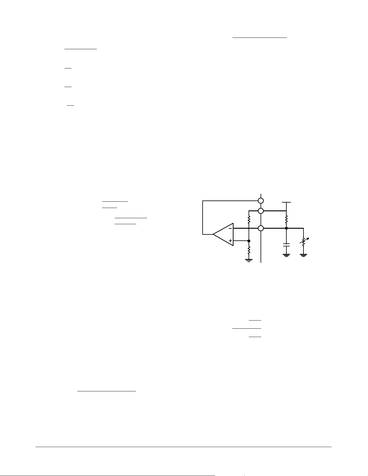
ADP3212A, NCP3218A
The compensation values can be calculated as follows:
CA+
RA+
CB+
CFB+
n RO T
RE R
T
C
C
A
T
B
R
B
T
D
R
A
A
B
(eq. 31)
(eq. 32)
(eq. 33)
(eq. 34)
The standard values for these components are subject to
the tuning procedure described in the Tuning Procedure for
12 section.
CIN Selection and Input Current di/dt Reduction
In continuous inductor−current mode, the source current
of the high−side MOSFET is approximately a square wave
with a duty ratio equal to n × V
that is one−n
th
of the maximum output current. To prevent
OUT/VIN
and an amplitude
large voltage transients, use a low ESR input capacitor sized
for the maximum rms current. The maximum rms capacitor
current occurs at the lowest input voltage and is given by:
1
I
+ D IO
CRMS
I
+ 0.18 40 A
CRMS
Ǹ
n D
* 1
1
2 0.18
(eq. 35)
* 1Ǹ+ 9.6 A
where IO is the output current.
In a typical notebook system, the battery rail decoupling
is achieved by using MLC capacitors or a mixture of MLC
capacitors and bulk capacitors. In this example, the input
capacitor bank is formed by eight pieces of 10 mF, 25 V MLC
capacitors, with a ripple current rating of about 1.5 A each.
RC Snubber
It is important in any buck topology to use a
resistor−capacitor snubber across the low side power
MOSFET. The RC snubber dampens ringing on the switch
node when the high side MOSFET turns on. The switch node
ringing could cause EMI system failures and increased
stress on the power components and controller. The RC
snubber should be placed as close as possible to the low side
MOSFET. Typical values for the resistor range from 1 W to
10 W. Typical values for the capacitor range from 330 pF to
4.7 nF. The exact value of the RC snubber depends on the
PCB layout and MOSFET selection. Some fine tuning must
be done to find the best values. The equation below is used
to find the starting values for the RC subber.
R
Snubber
+
2 p f
1
Ringing
C
OSS
(eq. 36)
C
P
Where R
C
Snubber
f
Rininging
+
Snubber
Snubber
Snubber
is the snubber capacitor.
p f
+ C
Snubber
is the snubber resistor.
Ringing
V
1
R
Input
Snubber
2
f
Switching
is the frequency of the ringing on the switch node
(eq. 37)
(eq. 38)
when the high side MOSFET turns on.
C
is the low side MOSFET output capacitance at V
OSS
Input
This is taken from the low side MOSFET data sheet.
V
is the input voltage.
input
f
Switching
P
is the switching frequency.
is the power dissipated in R
Snubber
Snubber
.
Selecting Thermal Monitor Components
To monitor the temperature of a single−point hot spot, set
R
equal to the NTC thermistor’s resistance at the alarm
TTSET1
temperature. For example, if the alarm temperature for VRTT
is 100°C and a Vishey thermistor (NTHS−0603N011003J)
with a resistance of 100 kW at 25°C, or 6.8 kW at 100°C, is
used, the user can set R
equal to 6.8 kW (the R
TTSET1
TH1
at
100°C).
5 V
VRTT
VCC
ADP3212
R
TTSNS
R
R
TTSET1
R
C
TT
TH1
Figure 33. Single−Point Thermal Monitoring
To monitor the temperature of multiple−point hot spots,
use the configuration shown in Figure 34. If any of the
monitored hot spots reaches the alarm temperature, the
VRTT signal is asserted. The following calculation sets the
alarm temperature:
V
FD
V
REF
R
V
FD
V
REF
TH1AlarmTemperature
(eq. 39)
R
TTSET1
1ń2 )
+
1ń2 *
where VFD is the forward drop voltage of the parallel diode.
Because the forward current is very small, the forward
drop voltage is very low, that is, less than 100 mV. Assuming
the same conditions used for the single−point thermal
monitoring example—that is, an alarm temperature of
100°C and use of an NTHS−0603N011003J Vishay
thermistor—solving Equation 39 gives a R
TTSET
of 7.37 kW,
and the closest standard resistor is 7.32 kW (1%).
.
http://onsemi.com
30
Page 31
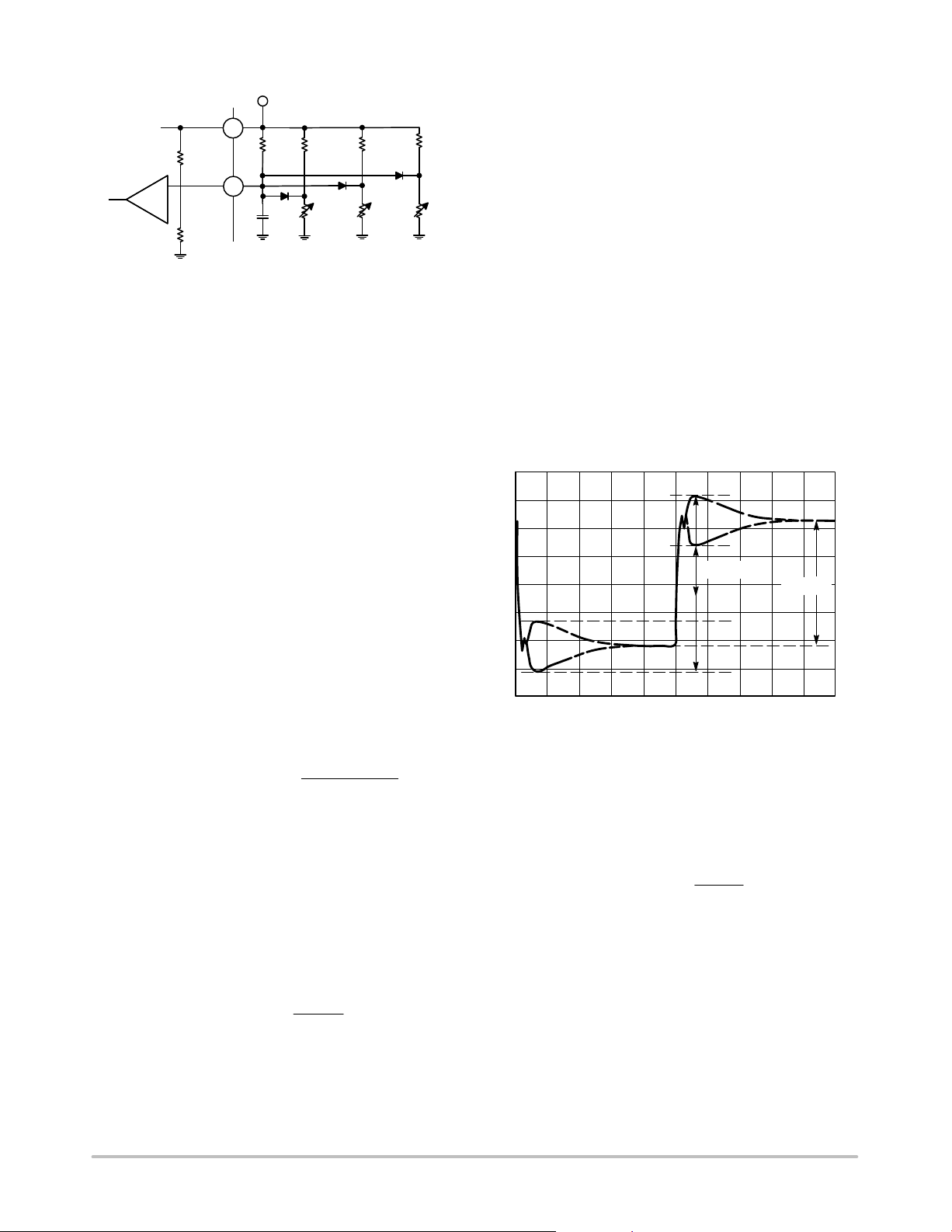
ADP3212A, NCP3218A
5 V
VCC
37
ADP3212
VRTT
Figure 34. Multiple−Point Thermal Monitoring
−
+
R
TTSNS
R
11
R
TTSET1RTTSET2
R
C
TH1
TT
R
TTSET3
R
TH3
R
TH2
The number of hot spots monitored is not limited. The
alarm temperature of each hot spot can be individually set by
using different values for R
TTSET1
, R
TTSET2
, ... R
TTSETn
.
Tuning Procedure for APD3212A/NCP3218A
Set Up and Test the Circuit
1. Build a circuit based on the compensation values
computed from the design spreadsheet.
2. Connect a dc load to the circuit.
3. Turn on the APD3212A/NCP3218A and verify
that it operates properly.
4. Check for jitter with no load and full load
conditions.
7. Measure the output ripple with no load and with a
full load with scope, making sure both are within
the specifications.
Set the AC Load Line
1. Remove the dc load from the circuit and connect a
dynamic load.
2. Connect the scope to the output voltage and set it
to dc coupling mode with a time scale of
100 ms/div.
3. Set the dynamic load for a transient step of about
40 A at 1 kHz with 50% duty cycle.
4. Measure the output waveform (note that use of a
dc offset on the scope may be necessary to see the
waveform). Try to use a vertical scale of
100 mV/div or finer.
5. The resulting waveform will be similar to that
shown in Figure 35. Use the horizontal cursors to
measure V
ACDRP
and V
DCDRP
, as shown in
Figure 35. Do not measure the undershoot or
overshoot that occurs immediately after the step.
Set the DC Load Line
1. Measure the output voltage with no load (VNL)
and verify that this voltage is within the specified
tolerance range.
2. Measure the output voltage with a full load when
the device is cold (V
FLCOLD
). Allow the board to
run for ~10 minutes with a full load and then
measure the output when the device is hot
(V
). If the difference between the two
FLHOT
measured voltages is more than a few millivolts,
adjust R
R
CS2(NEW)
3. Repeat Step 2 until no adjustment of R
using Equation 40.
CS2
+ R
CS2(OLD)
VNL* V
VNL* V
FLCOLD
FLHOT
CS2
needed.
4. Compare the output voltage with no load to that
with a full load using 5 A steps. Compute the load
line slope for each change and then find the
average to determine the overall load line slope
(R
5. If the difference between R
OMEAS
).
and RO is more
OMEAS
than 0.05 mW, use the following equation to adjust
PH
PH(NEW)
values:
+ R
PH(OLD)
R
OMEAS
R
O
the R
R
6. Repeat Steps 4 and 5 until no adjustment of RPH is
needed. Once this is achieved, do not change R
R
, R
CS1
, or RTH for the rest of the procedure.
CS2
(eq. 40)
is
(eq. 41)
PH
V
Figure 35. AC Load Line Waveform
6. If the difference between V
ACDRP
ACDRP
and V
V
DCDRP
DCDRP
is
more than a couple of millivolts, use Equation 42
to adjust C
. It may be necessary to try several
CS
parallel values to obtain an adequate one because
there are limited standard capacitor values
available (it is a good idea to have locations for
two capacitors in the layout for this reason).
C
CS(NEW)
+ C
CS(OLD)
ACDRP
V
DCDRP
(eq. 42)
V
7. Repeat Steps 5 and 6 until no adjustment of CCS is
needed. Once this is achieved, do not change C
CS
for the rest of the procedure.
8. Set the dynamic load step to its maximum step size
(but do not use a step size that is larger than
needed) and verify that the output waveform is
square, meaning V
ACDRP
and V
DCDRP
are equal.
9. Ensure that the load step slew rate and the
,
powerup slew rate are set to ~150 A/ms to
250 A/ms (for example, a load step of 50 A should
http://onsemi.com
31
Page 32
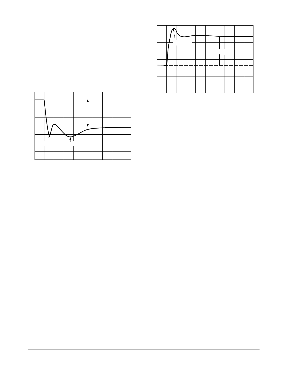
ADP3212A, NCP3218A
take 200 ns to 300 ns) with no overshoot. Some
dynamic loads have an excessive overshoot at
powerup if a minimum current is incorrectly set
(this is an issue if a VTT tool is in use).
Set the Initial Transient
1. With the dynamic load set at its maximum step
size, expand the scope time scale to 2 ms/div to
5 ms/div. This results in a waveform that may have
two overshoots and one minor undershoot before
achieving the final desired value after V
(see Figure 36).
V
DROOP
V
TRAN1
Figure 36. Transient Setting Waveform, Load Step
V
TRAN2
2. If both overshoots are larger than desired, try the
following adjustments in the order shown.
a. Increase the resistance of the ramp resistor
(R
b. For V
) by 25%.
RAMP
, increase CB or increase the switching
TRAN1
frequency.
c. For V
, increase RA by 25% and decrease C
TRAN2
by 25%.
If these adjustments do not change the response, it is
because the system is limited by the output
decoupling. Check the output response and the
switching nodes each time a change is made to
ensure that the output decoupling is stable.
3. For load release (see Figure 37), if V
larger than the value specified by IMVP−6.5, a
greater percentage of output capacitance is needed.
Either increase the capacitance directly or decrease
the inductor values. (If inductors are changed,
however, it will be necessary to redesign the
circuit using the information from the spreadsheet
and to repeat all tuning guide procedures).
DROOP
TRANREL
is
V
TRANREL
V
DROOP
Figure 37. Transient Setting Waveform, Load Release
Layout and Component Placement
The following guidelines are recommended for optimal
performance of a switching regulator in a PC system.
General Recommendations
1. For best results, use a PCB of four or more layers.
This should provide the needed versatility for
control circuitry interconnections with optimal
placement; power planes for ground, input, and
output; and wide interconnection traces in the rest
of the power delivery current paths. Keep in mind
that each square unit of 1 oz copper trace has a
resistance of ~0.53 mW at room temperature.
2. When high currents must be routed between PCB
layers, vias should be used liberally to create
several parallel current paths so that the resistance
and inductance introduced by these current paths is
minimized and the via current rating is not
A
exceeded.
3. If critical signal lines (including the output voltage
sense lines of the APD3212A/NCP3218A) must
cross through power circuitry, it is best if a signal
ground plane can be interposed between those
signal lines and the traces of the power circuitry.
This serves as a shield to minimize noise injection
into the signals at the expense of increasing signal
ground noise.
4. An analog ground plane should be used around
and under the APD3212A/NCP3218A for
referencing the components associated with the
controller. This plane should be tied to the nearest
ground of the output decoupling capacitor, but
should not be tied to any other power circuitry to
prevent power currents from flowing into the
plane.
http://onsemi.com
32
Page 33

ADP3212A, NCP3218A
5. The components around the
APD3212A/NCP3218A should be located close to
the controller with short traces. The most
important traces to keep short and away from other
traces are those to the FB and CSSUM pins. Refer
to Figure 30 for more details on the layout for the
CSSUM node.
6. The output capacitors should be connected as close
as possible to the load (or connector) that receives
the power (for example, a microprocessor core). If
the load is distributed, the capacitors should also
be distributed and generally placed in greater
proportion where the load is more dynamic.
7. Avoid crossing signal lines over the switching
power path loop, as described in the Power
Circuitry section.
8. Connect a 1 mF decoupling ceramic capacitor from
VCC to GND. Place this capacitor as close as
possible to the controller. Connect a 4.7 mF
decoupling ceramic capacitor from PVCC to
PGND. Place capacitor as close as possible to the
controller.
Power Circuitry
1. The switching power path on the PCB should be
routed to encompass the shortest possible length to
minimize radiated switching noise energy (that is,
EMI) and conduction losses in the board. Failure
to take proper precautions often results in EMI
problems for the entire PC system as well as
noise−related operational problems in the
power−converter control circuitry. The switching
power path is the loop formed by the current path
through the input capacitors and the power
MOSFETs, including all interconnecting PCB
traces and planes. The use of short, wide
interconnection traces is especially critical in this
path for two reasons: it minimizes the inductance
in the switching loop, which can cause high energy
ringing, and it accommodates the high current
demand with minimal voltage loss.
2. When a power−dissipating component (for
example, a power MOSFET) is soldered to a PCB,
the liberal use of vias, both directly on the
mounting pad and immediately surrounding it, is
recommended. Two important reasons for this are
improved current rating through the vias and
improved thermal performance from vias extended
to the opposite side of the PCB, where a plane can
more readily transfer heat to the surrounding air.
To achieve optimal thermal dissipation, mirror the
pad configurations used to heat sink the MOSFETs
on the opposite side of the PCB. In addition,
improvements in thermal performance can be
obtained using the largest possible pad area.
3. The output power path should also be routed to
encompass a short distance. The output power path
is formed by the current path through the inductor,
the output capacitors, and the load.
4. For best EMI containment, a solid power ground
plane should be used as one of the inner layers and
extended under all power components.
Signal Circuitry
1. The output voltage is sensed and regulated
between the FB and FBRTN pins, and the traces of
these pins should be connected to the signal
ground of the load. To avoid differential mode
noise pickup in the sensed signal, the loop area
should be as small as possible. Therefore, the FB
and FBRTN traces should be routed adjacent to
each other, atop the power ground plane, and back
to the controller.
2. The feedback traces from the switch nodes should
be connected as close as possible to the inductor.
The CSREF signal should be Kelvin connected to
the center point of the copper bar, which is the
V
common node for the inductors of all the
CORE
phases.
3. On the back of the APD3212A/NCP3218A
package, there is a metal pad that can be used to
heat sink the device. Therefore, running vias under
the APD3212A/NCP3218A is not recommended
because the metal pad may cause shorting between
vias.
ORDERING INFORMATION
Device Number* Temperature Range Package Package Option Shipping
ADP3212AMNR2G −40°C to 100°C 48−Lead Frame Chip Scale Pkg [QFN_VQ]
7x7 mm, 0.5 mm pitch
NCP3218AMNR2G −40°C to 100°C 48−Lead Frame Chip Scale Pkg [QFN_VQ]
6x6 mm, 0.4 mm pitch
†For information on tape and reel specifications, including part orientation and tape sizes, please refer to our Tape and Reel Packaging
Specification Brochure, BRD8011/D.
*The “G’’ suffix indicates Pb−Free package.
http://onsemi.com
33
CP−48−1 2500 / Tape & Reel
CP−48−1 2500 / Tape & Reel
†
Page 34
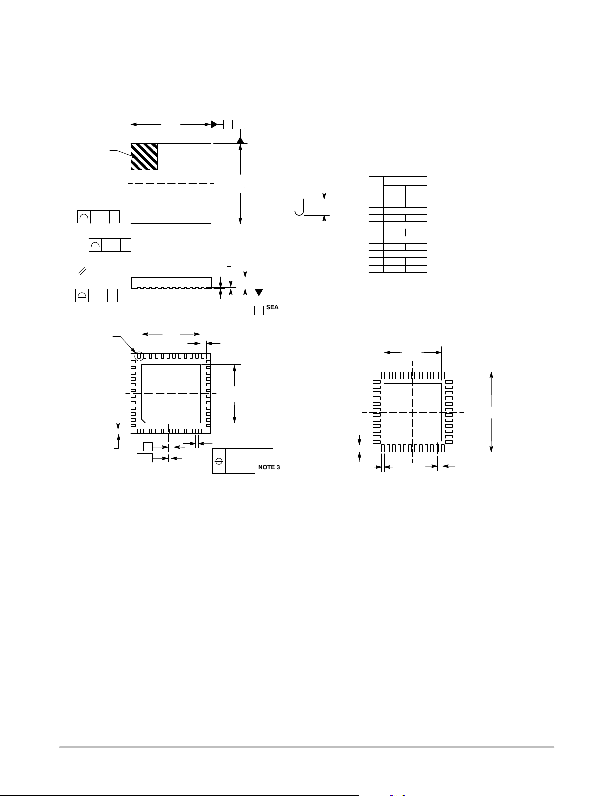
PIN 1
LOCATION
2X
0.15 C
2X
0.05 C
0.08 C
NOTE 4
0.15
C
D A B
TOP VIEW
SIDE VIEW
(A3)
A1
ADP3212A, NCP3218A
PACKAGE DIMENSIONS
QFN48 7x7, 0.5P
CASE 485AJ−01
ISSUE O
E
L
DETAIL A
OPTIONAL CONSTRUCTION
2X SCALE
A
SEATING
C
PLANE
NOTES:
1. DIMENSIONS AND TOLERANCING PER ASME
Y14.5M, 1994.
2. CONTROLLING DIMENSION: MILLIMETERS.
3. DIMENSION b APPLIES TO THE PLATED
TERMINAL AND IS MEASURED ABETWEEN
0.15 AND 0.30 MM FROM TERMINAL TIP.
4. COPLANARITY APPLIES TO THE EXPOSED
PAD AS WELL AS THE TERMINALS.
MILLIMETERS
DIM MIN MAX
A 0.80 1.00
A1 0.00 0.05
A3 0.20 REF
b 0.20 0.30
D 7.00 BSC
D2 5.00 5.20
E 7.00 BSC
E2 5.00 5.20
e 0.50 BSC
K 0.20 −−−
L 0.30 0.50
DETAIL A
48X
13
12
1
48 37
L
e/2
D2
e
BOTTOM VIEW
36
25
48X
K
1
E2
48X
0.63
b
0.10
C
A B
NOTE 3
0.05
C
*For additional information on our Pb−Free strategy and soldering
details, please download the ON Semiconductor Soldering and
Mounting Techniques Reference Manual, SOLDERRM/D.
48X
0.30
2X
5.20
0.50 PITCH
DIMENSIONS: MILLIMETERS
2X
7.30
SOLDERING FOOTPRINT*
http://onsemi.com
34
Page 35
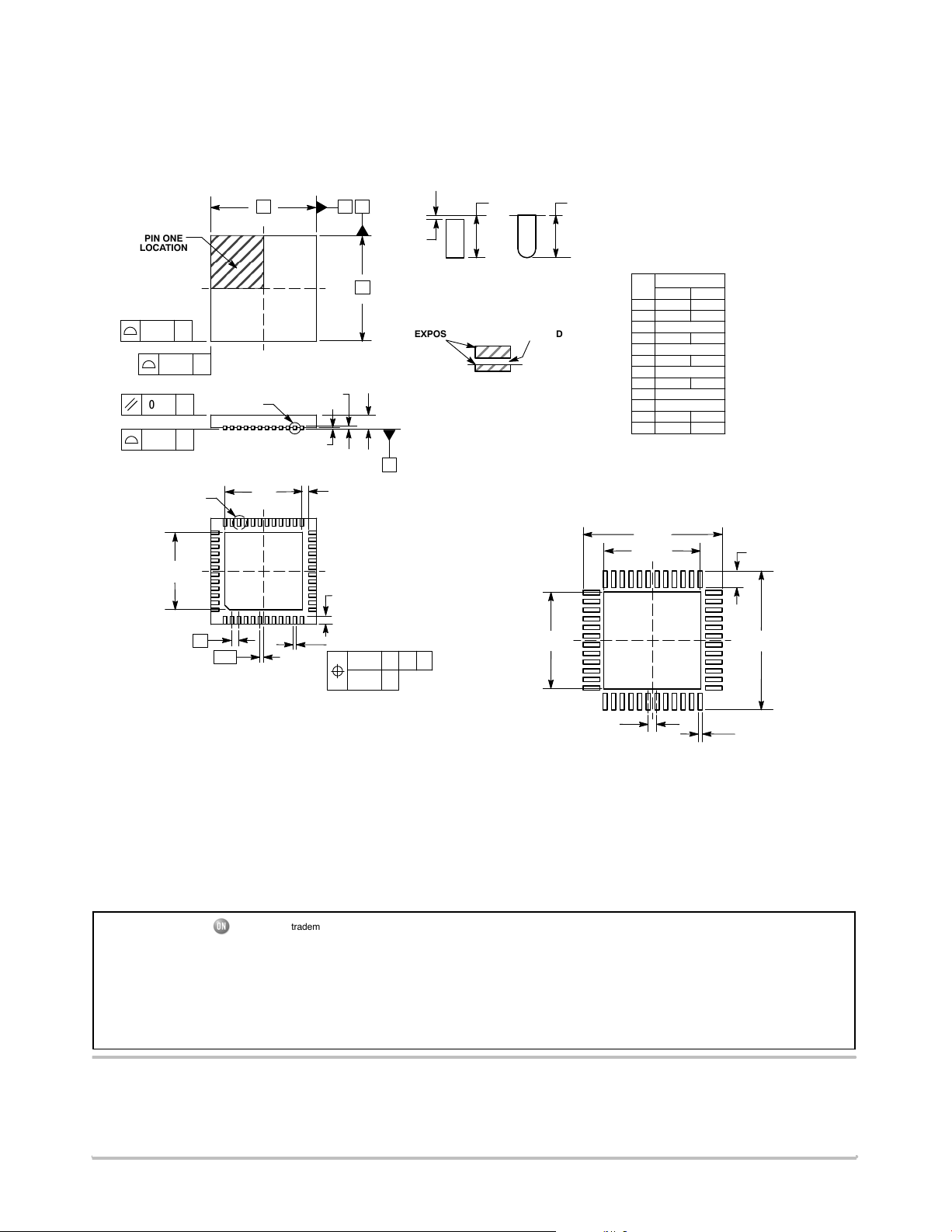
2X
LOCATION
2X
NOTE 4
PIN ONE
0.15 C
0.15
0.10 C
0.08 C
DETAIL A
E2
TOP VIEW
C
DETAIL B
SIDE VIEW
13
1
40
e
e/2
BOTTOM VIEW
D
D2
ADP3212A, NCP3218A
PACKAGE DIMENSIONS
QFN48 6x6, 0.4P
CASE 485AN−01
ISSUE O
NOTES:
1. DIMENSIONING AND TOLERANCING PER
A B
L
L
L1
DETAIL A
ALTERNATE TERMINAL
CONSTRUCTIONS
MOLD CMPDEXPOSED Cu
DETAIL B
ALTERNATE
CONSTRUCTION
(A3)
E
A
A1
SEATING
C
PLANE
K
SOLDERING FOOTPRINT*
25
L
37
48X
b
0.05
C
C
A0.10 B
NOTE 3
4.56
ASME Y14.5M, 1994.
2. CONTROLLING DIMENSIONS: MILLIMETERS.
3. DIMENSION b APPLIES TO PLATED
TERMINAL AND IS MEASURED BETWEEN
0.15 AND 0.30mm FROM TERMINAL TIP
4. COPLANARITY APPLIES TO THE EXPOSED
PAD AS WELL AS THE TERMINALS.
MILLIMETERS
DIM MIN MAX
A 0.70 0.80
A1 0.00 0.05
A3 0.20 REF
b 0.15 0.25
D 6.00 BSC
D2 4.25 4.55
E 6.00 BSC
e 0.40 BSC
K 0.20 MIN
L 0.35 0.55
L1 0.00 0.15
6.40
4.56
4.55E2 4.25
48X
0.73
6.40
0.40
PITCH
DIMENSIONS: MILLIMETERS
48X
0.25
*For additional information on our Pb−Free strategy and soldering
details, please download the ON Semiconductor Soldering and
Mounting Techniques Reference Manual, SOLDERRM/D.
All brand names and product names appearing in this document are registered trademarks or trademarks of their respective holders.
ON Semiconductor and are registered trademarks of Semiconductor Components Industries, LLC (SCILLC). SCILLC reserves the right to make changes without further notice
to any products herein. SCILLC makes no warranty, representation or guarantee regarding the suitability of its products for any particular purpose, nor does SCILLC assume any liability
arising out of the application or use of any product or circuit, and specifically disclaims any and all liability, including without limitation special, consequential or incidental damages.
“Typical” parameters which may be provided in SCILLC data sheets and/or specifications can and do vary in different applications and actual performance may vary over time. All
operating parameters, including “Typicals” must be validated for each customer application by customer’s technical experts. SCILLC does not convey any license under its patent rights
nor the rights of others. SCILLC products are not designed, intended, or authorized for use as components in systems intended for surgical implant into the body, or other applications
intended to support or sustain life, or for any other application in which the failure of the SCILLC product could create a situation where personal injury or death may occur. Should
Buyer purchase or use SCILLC products for any such unintended or unauthorized application, Buyer shall indemnify and hold SCILLC and its officers, employees, subsidiaries, affiliates,
and distributors harmless against all claims, costs, damages, and expenses, and reasonable attorney fees arising out of, directly or indirectly, any claim of personal injury or death
associated with such unintended or unauthorized use, even if such claim alleges that SCILLC was negligent regarding the design or manufacture of the part. SCILLC is an Equal
Opportunity/Affirmative Action Employer. This literature is subject to all applicable copyright laws and is not for resale in any manner.
PUBLICATION ORDERING INFORMATION
LITERATURE FULFILLMENT:
Literature Distribution Center for ON Semiconductor
P.O. Box 5163, Denver, Colorado 80217 USA
Phone: 303−675−2175 or 800−344−3860 Toll Free USA/Canada
Fax: 303−675−2176 or 800−344−3867 Toll Free USA/Canada
Email: [email protected]
N. American Technical Support: 800−282−9855 Toll Free
USA/Canada
Europe, Middle East and Africa Technical Support:
Phone: 421 33 790 2910
Japan Customer Focus Center
Phone: 81−3−5773−3850
http://onsemi.com
ON Semiconductor Website: www.onsemi.com
Order Literature: http://www.onsemi.com/orderlit
For additional information, please contact your local
Sales Representative
ADP3212A/D
35
 Loading...