

Page 1
NCP1608BOOSTGEVB
NCP1608 100 W Boost
Evaluation Board User's
Manual
http://onsemi.com
Introduction
The NCP1608 is a voltage mode power factor correction
(PFC) controller designed to implement converters to
comply with line current harmonic regulations. The device
operates in critical conduction mode (CrM) for optimal
performance in applications up to 350 W. Its voltage mode
scheme enables it to obtain near unity power factor (PF)
without the need for a line-sensing network. The output
voltage is accurately controlled with an integrated high
precision transconductance error amplifier. The controller
also implements a comprehensive set of safety features that
simplify system design.
This application note describes the design and
implementation of a 400 V, 100 W, CrM boost PFC
converter using the NCP1608. The converter exhibits high
PF, low standby power dissipation, high active mode
efficiency, and a variety of protection features.
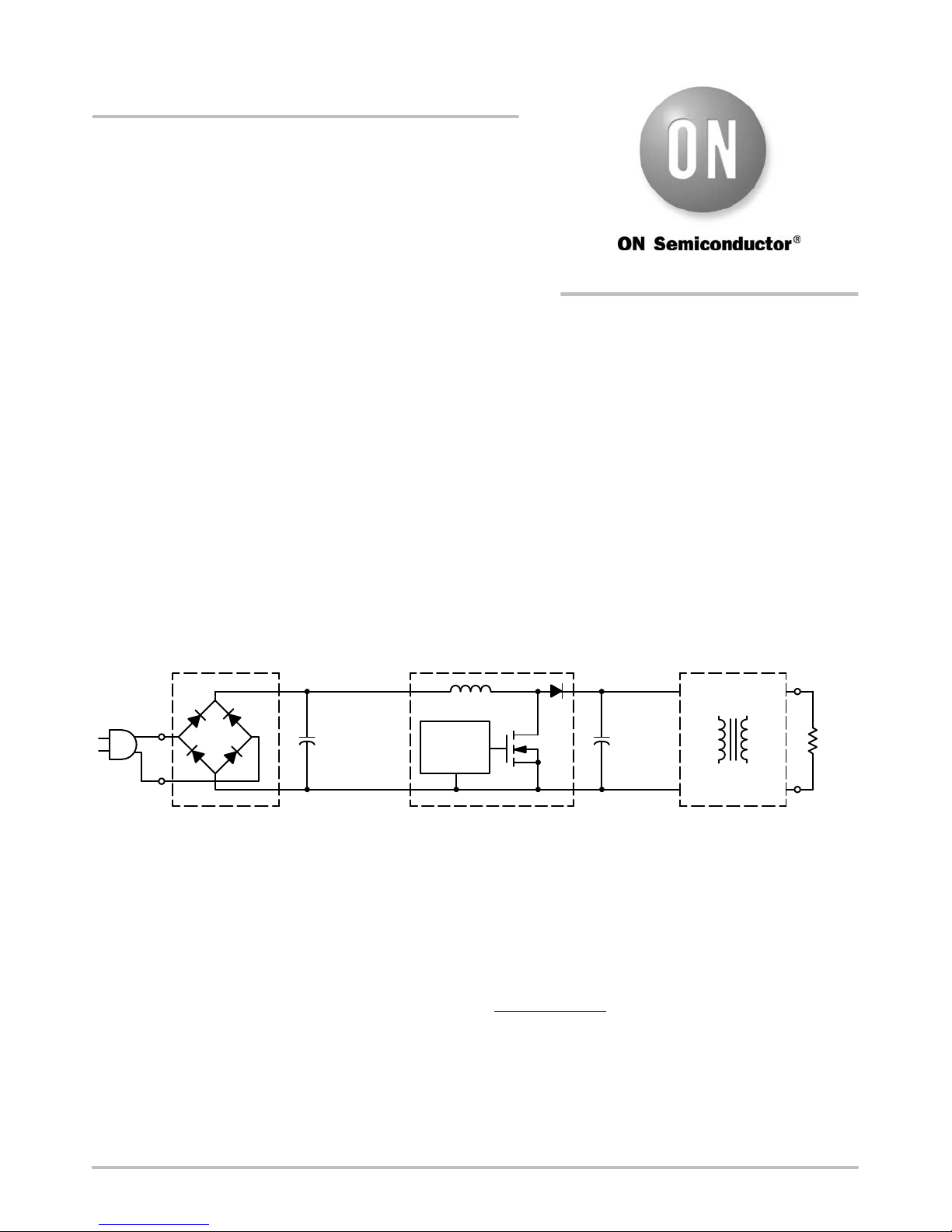
PFC Pre−Converter
NCP1608
AC Line
Rectifiers
+
High
Frequency
Bypass
Capacitor
EVAL BOARD USER’S MANUAL
The Need for PFC
Most electronic ballasts and switch−mode power supplies
(SMPS) use a diode bridge rectifier and a bulk storage
capacitor to produce a dc voltage from the utility ac line.
This causes a non-sinusoidal current consumption and
increases the stress on the power delivery infrastructure.
Government regulations and utility requirements mandate
control over line current harmonic content. Active PFC
circuits are the most popular method to comply with these
harmonic content requirements. System solutions consist of
connecting a PFC pre−converter between the rectifier bridge
and the bulk capacitor (Figure 1). The boost converter is the
most popular topology for active PF correction. It produces
a constant output voltage and consumes a sinusoidal input
current from the line.
Converter
Bulk
+
Storage
Capacitor
Load
Basic Operation of a CrM Boost Converter
For medium power (< 350 W) applications, CrM is the
preferred control method. CrM operates at the boundary
between discontinuous conduction mode (DCM) and
continuous conduction mode (CCM). In CrM, the drive on
time begins when the inductor current reaches zero.
CrM combines the reduced peak current of CCM
operation with the zero current switching of DCM
© Semiconductor Components Industries, LLC, 2012
November, 2012 − Rev. 1
Figure 1. Active PFC Stage with the NCP1608
operation. This control method causes the frequency to vary
with the instantaneous line input voltage (V
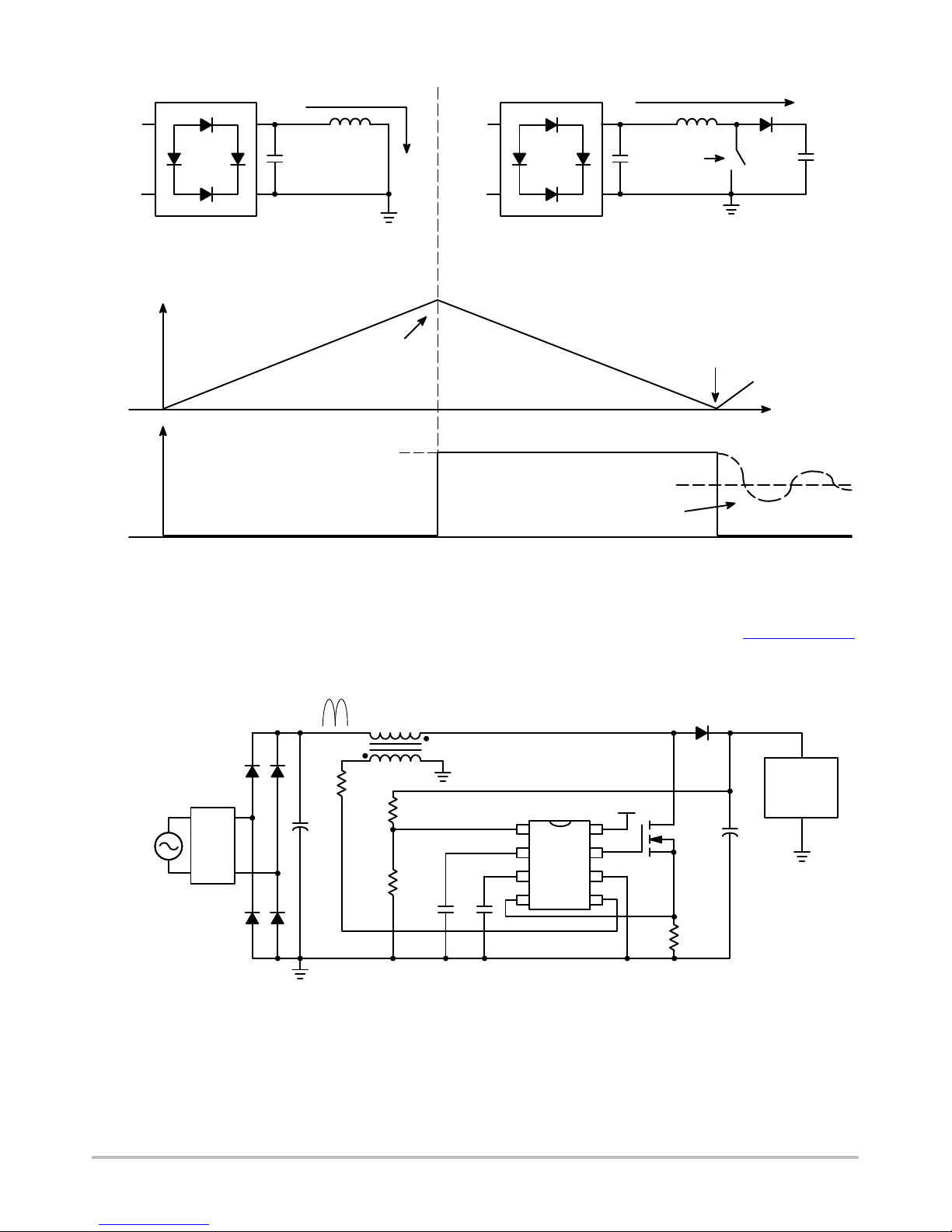
load. The operation and waveforms of a CrM PFC boost
converter are illustrated in Figure 2. For detailed
information on the operation of a CrM boost converter for
PFC applications, please refer to AND8123 at
www.onsemi.com
1 Publication Order Number:
.
) and the output
in
EVBUM2162/D
Page 2
NCP1608BOOSTGEVB
Diode Bridge
V
in
AC Line
+
+
L
−
The power switch is ON The power switch is OFF
With the power switch voltage being about zero, the
input voltage is applied across the inductor. The inductor current linearly increases with a (Vin/L) slope.
Inductor
Current
Vin/L
I
V
drain
V
out
I
L
V
drain
L(peak)
Diode Bridge
V
in
+
V
drain
L
+
AC Line
−
The inductor current flows through the diode. The inductor
voltage is (V
with a (V
− Vin) and the inductor current linearly decays
out
− Vin)/L slope.
out
(V
− Vin)/L
out
Critical Conduction Mode:
Next current cycle starts
when the core is reset.
V
in
If next cycle does not start
then V
rings towards V
drain
in
I
L
+
V
out
Figure 2. Schematic and Waveforms of an Ideal CrM Boost Converter
Features of the NCP1608
The NCP1608 is an excellent controller for robust
medium power CrM boost PFC applications due to its
integrated safety features, low impedance driver, high
precision error amplifier, and low standby current
consumption.
AC Line
EMI
Filter
V
in
R
ZCD
+
C
in
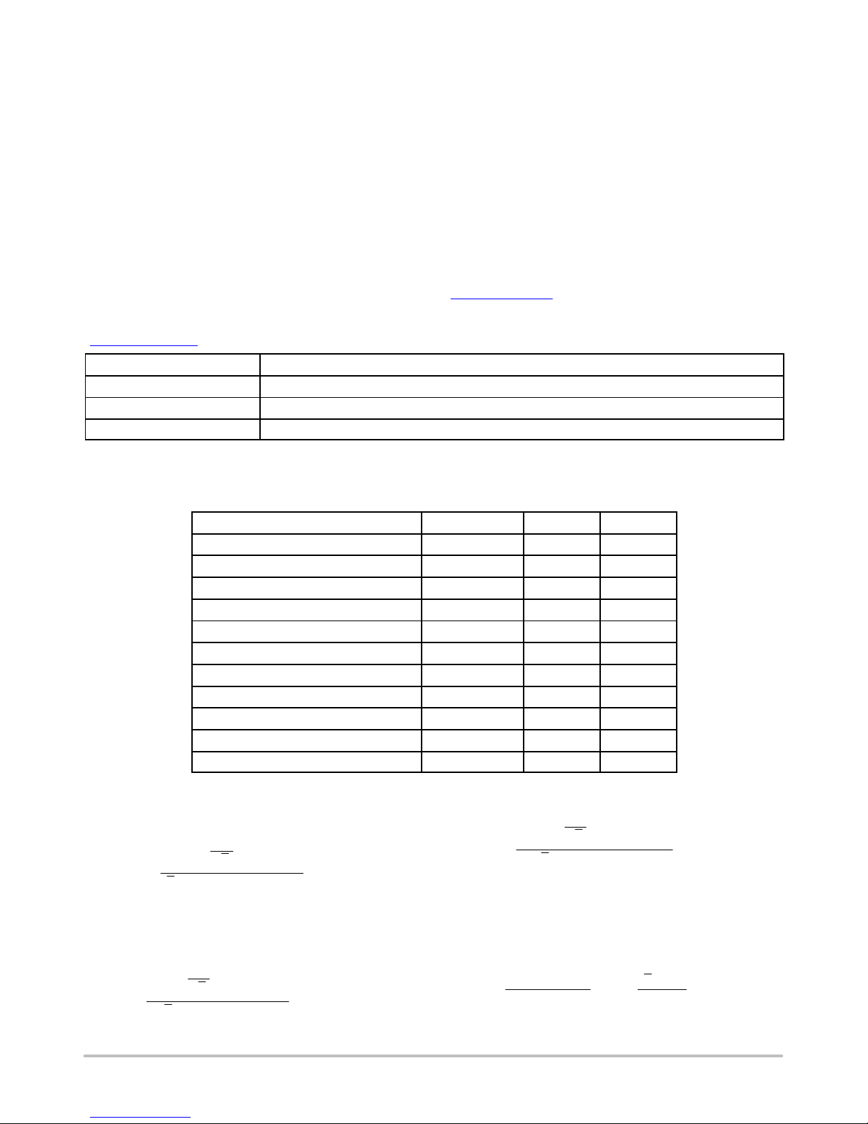
Figure 3. CrM Boost PFC Stage Featuring the NCP1608
L
R
out1
R
out2
C
COMP
For detailed information on the operation of the
NCP1608, please refer to NCP1608/D at www.onsemi.com
A CrM boost pre-converter featuring the NCP1608 is
shown in Figure 3.
M
R
D
sense
+
C
bulk
NB:N
C
t
ZCD
1
2
3
4
NCP1608
V
FB
Control
DRV
CtCSGND
ZCD
V
CC
8
CC
7
6
5
V
out
LOAD
(Ballast,
SMPS, etc.)
.
The FB pin senses the boost output voltage through the
resistor divider formed by R
out1
and R
includes overvoltage protection (OVP), undervoltage
protection (UVP), and floating pin protection (FPP). This
pin is the input to the error amplifier. The output of the error
amplifier is the Control pin.
. The FB pin
out2
A combination of resistors and capacitors connected
between the Control and ground pins forms a compensation
network that limits the bandwidth of the converter. For high
PF, the bandwidth is set to less than 20 Hz. A capacitor
connected to the Ct pin sets the maximum on time. The CS
pin provides cycle−by−cycle overcurrent protection. The
http://onsemi.com
2
Page 3
NCP1608BOOSTGEVB
internal comparator compares the voltage developed across
R
(VCS) to an internal reference (V
sense
turns off when V
reaches V
CS
. The ZCD pin senses the
ILIM
). The driver
ILIM
demagnetization of the boost inductor to turn on the drive.
The drive on time begins after the ZCD pin voltage (V
exceeds V
V
ZCD(TRIG)
ZCD(ARM)
. A resistor in series with the ZCD winding
and then decreases to less than
ZCD
)
limits the ZCD pin current.
The NCP1608 features a powerful output driver on the
DRV pin. The driver is capable of switching the gates of
large MOSFETs efficiently because of its low source and
sink impedances. The driver includes active and passive
pull−down circuits to prevent the output from floating high
when the NCP1608 is disabled.
Table 1. Additional Resources for the Design and Understanding of CrM Boost PFC Circuits Available at
www.onsemi.com
AND8123 Power Factor Correction Stages Operating in Critical Conduction Mode
AND8016 Design of Power Factor Correction Circuits Using the MC33260
AND8154 NCP1230 90 W, Universal Input Adapter Power Supply with Active PFC
HBD853 Power Factor Correction Handbook
DESIGN STEP 1: Define the Required Parameters
.
The V
is less than the turn on voltage (V
pin is the supply pin of the controller. When V
CC
CC(on)
consumption of the device is less than 35 mA. This results in
fast startup times and reduced standby power losses.
Design Procedure
The design of a CrM boost PFC converter is discussed in
many ON Semiconductor application notes. Table 1 lists
some examples.
This application note describes the design procedure for
a 400 V, 100 W converter using the features of the NCP1608.
A dedicated NCP1608 design tool that enables users to
determine component values quickly is available at
www.onsemi.com
.
The converter parameters are shown in Table 2.
CC
), the current
Table 2. CONVERTER PARAMETERS
Parameter Name Symbol Value Units
Minimum Line Input Voltage Vac
Maximum Line Input Voltage Vac
Minimum Line Frequency f
Maximum Line Frequency f
Output Voltage V
Full Load Output Current I
Full Load Output Power P
Maximum Output Voltage V
Minimum Switching Frequency f
Minimum Full Load Efficiency
Minimum Full Load Power Factor PF 0.9 −
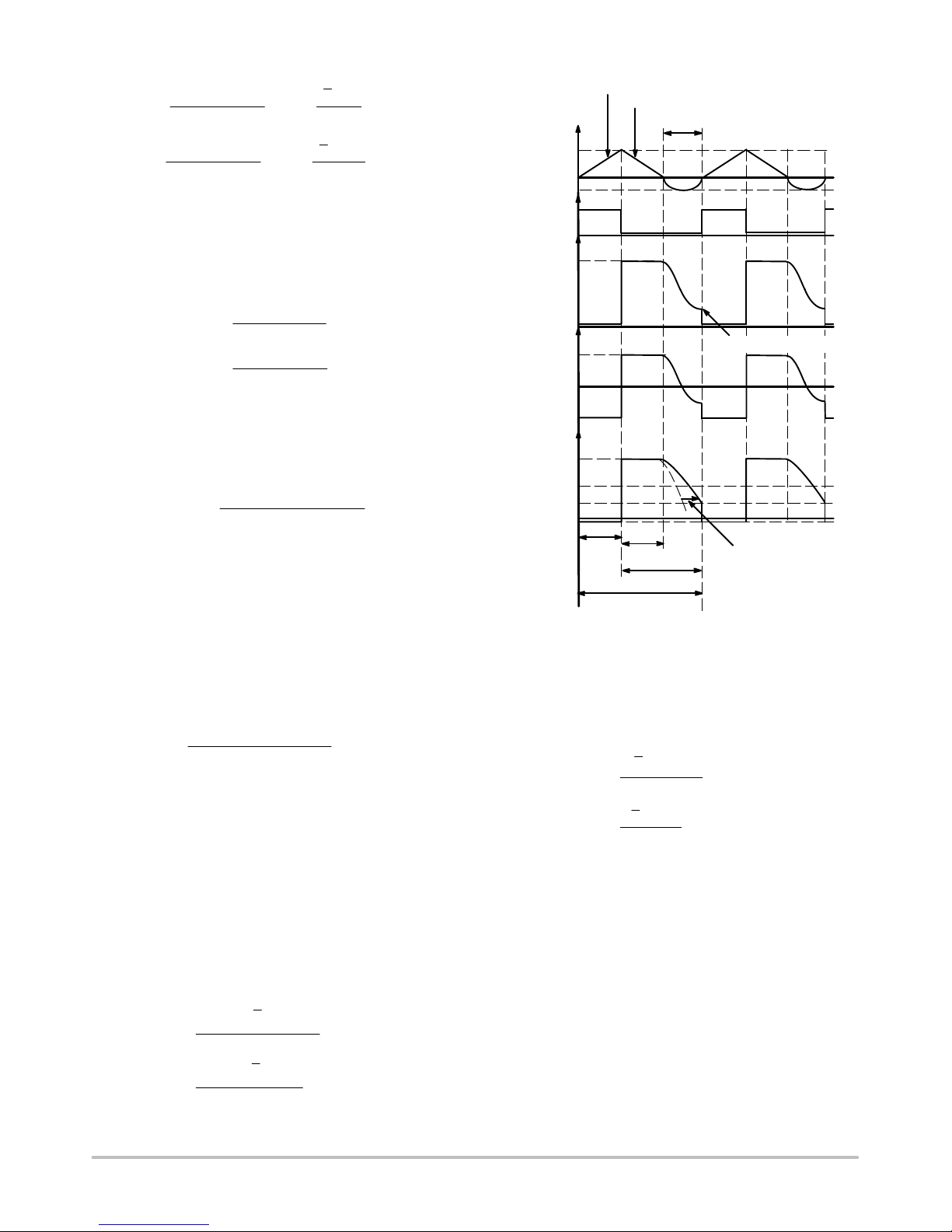
DESIGN STEP 2: Calculate the Boost Inductor
The value of the boost inductor (L) is calculated using
Equation 1:
V
out
2
ǒ
Vac
L v
@
Ǹ
@ V
2
out
* VacǓ@ h
Ǹ
2
@ P
out
@ f
SW(MIN)
(eq. 1)
To ensure that the switching frequency exceeds the
minimum frequency, L is calculated at both the minimum
and maximum rms input line voltage:
400
2
ǒ
85
LLLv
@
Ǹ
2
* 85Ǔ@ 0.92
Ǹ
2
@ 400 @ 100 @ 40 k
+ 581 mH
LL
HL
line(MIN)
line(MAX)
out
out
out
out(MAX)
SW(MIN)
h
Where LLLis the inductor value calculated at VacLL.
v
L
HL
Where L
85 Vac
265 Vac
47 Hz
63 Hz
400 V
250 mA
100 W
440 V
40 kHz
92 %
400
2
ǒ
265
@
Ǹ
2
is the inductor value calculated at VacHL.
HL
* 265Ǔ@ 0.92
Ǹ
2
@ 400 @ 100 @ 40 k
+ 509 mH
A value of 400 mH is selected. The inductance tolerance
is ±15%. The maximum inductance (L
MAX
) value is
460 mH. Equation 2 is used to calculate the minimum
frequency at full load.
fSW+
2 @ L
Vac
MAX
2
@ h
@ǒ1 *
@ P
out
Ǹ
@ Vac
2
V
out
Ǔ
(eq. 2)
http://onsemi.com
3
Page 4
NCP1608BOOSTGEVB
f
SW(LL)
f
SW(HL)
2
@ 0.92
85
+
2 @ 460 m @ 100
2
@ 0.92
265
+
2 @ 460 m @ 100
@ǒ1 *
@ǒ1 *
Ǹ
Ǹ
2
400
@ 265
2
400
@ 85
Ǔ
+ 50.5 kHz
Ǔ
+ 44.3 kHz
fSW is equal to 50.5 kHz at VacLL and 44.3 kHz at VacHL.
DESIGN STEP 3: Size the Ct Capacitor
The Ct capacitor is sized to set the maximum on time for
minimum line input voltage and maximum output power.
The maximum on time is calculated using Equation 3:
t
on(MAX)
t
on(MAX)
2 @ L
+
2 @ 460 m @ 100
+
MAX
h @ Vac
0.92 @ 85
@ P
LL
out
2
+ 13.8 ms
2
(eq. 3)
Sizing Ct to an excessively large value causes the
application to deliver excessive output power and reduces
the control range at Vac
or low output power. It is
HL
recommended to size the Ct capacitor to a value slightly
larger than that calculated by Equation 4:
Where I
charge
Ct w
and V
2 @ P
Ct(MAX)
@ L
out
h @ Vac
@ I
MAX
charge
2
@ V
LL
Ct(MAX)
are specified in the NCP1608
(eq. 4)
datasheet. To ensure that the controller sets the maximum on
time to a value sufficient to deliver the required output
power, the maximum I
and the minimum V
charge
Ct(MAX)
values are used in the calculations for Ct.
From the NCP1608 datasheet:
− V
− I
Ct(MAX)
charge
= 4.775 V (minimum)
= 297 mA (maximum)
Ct is equal to:
2 @ 100 @ 460 m @ 297 m
Ct w
0.92 @ 85
2
@ 4.775
+ 860 pF
A normalized value of 1 nF (±10%) provides sufficient
margin. A value of 1.22 nF is selected for Total Harmonic
Distortion (THD) reduction (see the Additional THD
Reduction section of this application note for more
information).
DESIGN STEP 4: Determine the ZCD Turns Ratio
To activate the ZCD detector of the NCP1608, the ZCD
turns ratio is sized such that at least V
ZCD(ARM)
(1.55 V
maximum) is applied to the ZCD pin during all operating
conditions (see Figure 4). The boost winding to ZCD
winding turns ratio (N = N
B:NZCD
) is calculated using
Equation 5.
N v
N v
V
*ǒ2Ǹ@ Vac
out
V
400 *
ZCD(ARM)
ǒ
2Ǹ@ 265
1.55
HL
Ǔ
+ 16
Ǔ
(eq. 5)
I
L(peak)
I
L(NEG)
DRV
V
V
ZCD(WIND)
V
ZCD(WIND),off
V
ZCD(WIND),on
V
V
CL(POS)
V
ZCD(ARM)
V
ZCD(TRIG)
V
CL(NEG)
MOSFET Conduction
I
L
drain
V
out
ZCD
Diode Conduction
t
diode
t
on
t
T
SW
t
z
0 A
0 V
0 V
Minimum Voltage Turn on
0 V
0 V
R
off
ZCD
Delay
Figure 4. Realistic CrM Waveforms Using a ZCD
Winding with R
A turns ratio of 10 is selected for this design. R
and the ZCD Pin Capacitance
ZCD
ZCD
is
connected between the ZCD winding and the ZCD pin to
limit the ZCD pin current. This current must be limited
below 10 mA. R
R
R
The value of R
is calculated using Equation 6:
ZCD
ZCD
ZCD
2Ǹ@ Vac
w
I
ZCD(MAX)
Ǹ
2
w
10 m @ 10
and the parasitic capacitance of the
ZCD
@ 265
HL
@ N
+ 3.75 kW
(eq. 6)
ZCD pin determine when the ZCD winding signal is
detected and the drive turn on begins. A large R
ZCD
value
creates a long delay before detecting the ZCD event. In this
case, the controller operates in DCM and the PF is reduced.
If the R
value is too small, the drive turns on when the
ZCD
drain voltage is high and efficiency is reduced. A popular
strategy for selecting R
is to use the R
ZCD
value that
ZCD
achieves minimum drain voltage turn on. This value is found
experimentally.
During the delay caused by R
capacitance, the equivalent drain capacitance (C
and the ZCD pin
ZCD
EQ(drain)
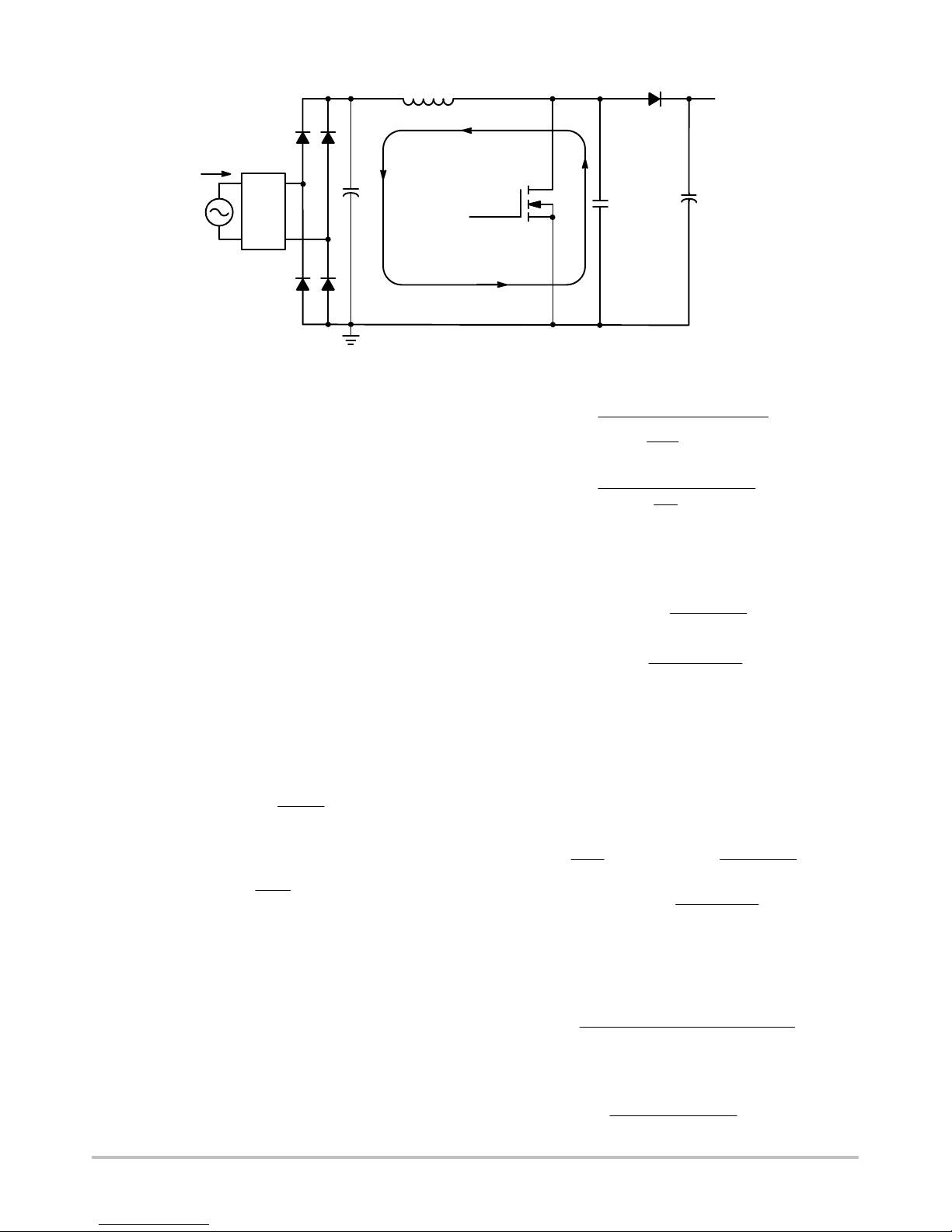
discharges through the path shown in Figure 5.
)
http://onsemi.com
4
Page 5
NCP1608BOOSTGEVB
L
I
L
I
AC Line
in
EMI
Filter
+
C
in
Figure 5. Equivalent Drain Capacitance Discharge Path
C
EQ(drain)
MOSFET, the diode, and the inductor. C
energy discharged by C
biases the bridge rectifier and causes the input current (I
is the combined parasitic capacitances of the
is charged by the
in
EQ(drain)
. The charging of Cin reverse
in
to decrease to zero. The zero input current causes THD to
increase. To reduce THD, the ratio (t
where t
turns on. The ratio (t
is the period from when IL = 0 A to when the drive
Z
/ TSW) is inversely proportional to the
z
/ TSW) is minimized,
z
square root of L.
DESIGN STEP 5: Set the FB, OVP, and UVP Levels
R
and R
out1
V
before it is applied to the FB pin. The error amplifier
out
form a resistor divider that scales down
out2
adjusts the on time of the drive to maintain the FB pin
voltage equal to the error amplifier reference voltage
(V
). The divider network bias current (I
REF
bias(out)
selection is the first step in the calculation. The divider
network bias current is selected to optimize the tradeoff of
noise immunity and power dissipation. R
is calculated
out1
using the optimized bias current and output voltage using
Equation 7:
V
+
out
I
bias(out)
R
out1
(eq. 7)
A bias current of 100 mA provides an acceptable tradeoff
of power dissipation to noise immunity.
+
400
100 m
+ 4MW
R
out1
The output voltage signal is delayed before it is applied to
the FB pin due to the time constant set by R
pin capacitance. R
must not be sized too large or this
out1
and the FB
out1
delay may cause overshoots of the OVP detection voltage.
R
is dependent on V
out2
feedback resistor (R
table). R
is calculated using Equation 8:
out2
, shown in the NCP1608 specification
FB
out
, R
, and the internal
out1
V
@ R
out
+
C
bulk
FB
out1
+ 25.3 kW
D
C
EQ(drain)
R
R
+
out2
RFB@
)
R
+
out2
4.6 M @
R
is selected as 25.5 kW for this design.
out2
out1
V
out
ǒ
* 1Ǔ* R
V
REF
4M@ 4.6 M
400
ǒ
* 1Ǔ* 4M
2.5
Using the selected resistor, the resulting output voltage is
calculated using Equation 9:
R
) R
V
+ V
out
V
+ 2.5 @ǒ4M@
)
out
REF
@ǒR
out2
@
out1
R
out2
25.5 k ) 4.6 M
25.5 k @ 4.6 M
FB
) 1
@ R
FB
) 1Ǔ+ 397 V
The low bandwidth of the PFC stage causes overshoots
during transient loads or during startup. The NCP1608
includes an integrated OVP circuit to prevent the output
from exceeding a safe voltage. The OVP circuit compares
V
to the internal overvoltage detect threshold voltage to
FB
determine if an OVP fault occurs. The OVP detection
voltage is calculated using Equation 10:
V
V
out(OVP)
V
out(OVP)
OVP
+
+ 1.06 @ 2.5 @ǒ4M@
@ V
V
REF
The output capacitor (C
REF
@ǒR
bulk
R
) R
out2
@
out1
R
@ R
out2
25.5 k ) 4.6 M
25.5 k @ 4.6 M
) 1Ǔ+ 421 V
) value is sized to be large
enough so that the peak-to-peak output voltage ripple
(V
ripple(peak-peak)
C
is calculated using Equation 11:
bulk
C
bulk
Where f
and V
line
ripple(peak-peak)
) is less than the OVP detection voltage.
P
w
2 @ p @ V
ripple(peak−peak)
out
@ f
line
@ V
= 47 Hz is the worst case for the ripple voltage
< 42 V.
C
w
bulk
2 @ p @ 42 @ 47 @ 400
100
+ 20 mF
(eq. 8)
Ǔ
(eq. 9)
(eq. 10)
FB
Ǔ
) 1
FB
(eq. 11)
out
http://onsemi.com
5
Page 6
NCP1608BOOSTGEVB
Ǹ
The value of C
V
ripple(peak-peak)
is selected as 68 mF to reduce
bulk
to less than 15 V. This results in a peak
output voltage of 406.25 V, which is less than the peak output
OVP detection voltage (421 V).
The NCP1608 includes undervoltage protection (UVP).
During startup, C
voltage. If C
bulk
charges to the peak of the ac line
bulk
does not charge to a minimum voltage, the
NCP1608 detects an UVP fault. The UVP detection voltage
is calculated using Equation 12:
V
out(UVP)
V
out(UVP)
+ V
+ 0.31 @ǒ4M@
UVP
@ǒR
out1
out2
@
R
out2
25.5 k ) 4.6 M
25.5 k @ 4.6 M
@ R
FB
FB
Ǔ
) 1
(eq. 12)
) 1Ǔ+ 49 V
R
) R
The UVP feature protects against open loop conditions in
the feedback loop. If the FB pin is inadvertently floating
(perhaps due to a bad solder joint), the coupling within the
system may cause V
V
< VFB < V
UVP
to be within the regulation range (i.e.
FB
). The controller responds by delivering
REF
maximum power. The output voltage increases and over
stresses the components. The NCP1608 includes a feature to
protect the system if FB is floating. The internal pull-down
resistor (R
) ensures that VFB is below the UVP threshold
FB
if the FB pin is floating.
If the FB pin floats during operation, V
decreasing from V
. The rate of decrease depends on R
REF
begins
FB
FB
and the FB pin parasitic capacitance. As VFB decreases,
V
V
increases, which causes the on time to increase until
Control
FB
< V
. When VFB < V
UVP
, the UVP fault is detected
UVP
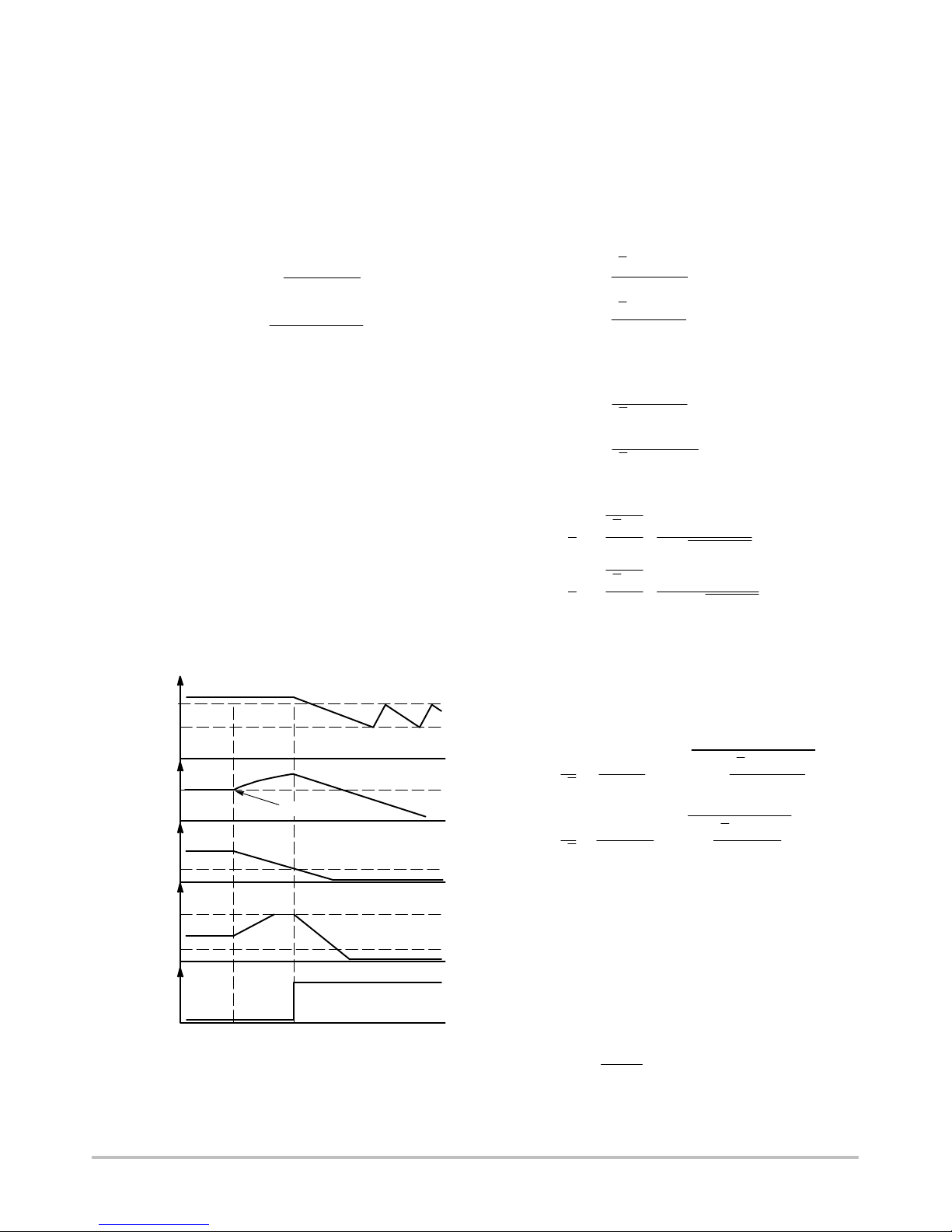
and the controller is disabled. The sequence is depicted in
Figure 6.
V
CC
V
CC(on)
V
CC(off)
V
out
V
out
Loop is Opened
V
FB
V
REF
V
UVP
V
Control
V
EAH
Ct
(offset)
UVP Fault
Figure 6. UVP Operation if Loop is Opened During
Operation
DESIGN STEP 6: Size the Power Components
The power components are sized such that there is
sufficient margin to sustain the currents and voltages applied
to them. At minimum line input voltage and maximum
output power the inductor peak current is at the maximum,
which causes the greatest stress to the power components.
The components are referenced in Figure 3.
1. The inductor peak current (I
L(peak)
) is calculated
using Equation 13:
+
Ǹ
+
2Ǹ@ 2 @ P
2
0.92 @ 85
I
L(peak)
I
L(peak)
The inductor rms current (I
h @ Vac
@ 2 @ 100
out
+ 3.62 A
L(RMS)
(eq. 13)
) is calculated using
Equation 14:
2 @ P
I
+
L(RMS)
I
+
L(RMS)
Ǹ
2. The output diode (D) rms current (I
out
3Ǹ@ Vac @ h
2 @ 100
@ 85 @ 0.92
3
+ 1.48 A
D(RMS)
(eq. 14)
) is
calculated using Equation 15:
I
D(RMS)
I
D(RMS)
+
+
Ǹ
@
3
4
3
p
Ǹ
@ 2
2
Ǹ
@
p
Ǹ
@ 2
2
4
The diode maximum voltage is equal to V
P
@
@
out
Ǹ
h @ Vac @ V
100
Ǹ
0.92 @ 85 @ 400
out
+ 0.75 A
(421 V)
OVP
(eq. 15)
plus the overshoot caused by parasitic contributions. For this
evaluation board, the maximum voltage is 450 V. A 600 V
diode provides a 25% derating factor. The MUR460
(4 A/600 V) diode is selected for this design.
3. The MOSFET (M) rms current (I
M(RMS)
) is
calculated using Equation 16:
P
I
M(RMS)
I
M(RMS)
+
+
2
Ǹ
3
2
Ǹ
3
ǒ
@
h @ Vac
ǒ
@
0.92 @ 85
out
100
Ǔ
@ 1 *
Ǹ
Ǔ
@ 1−
The MOSFET maximum voltage is equal to V
2Ǹ@ 8 @ Vac
ǒ
3 @ p @ V
2Ǹ@ 8 @ 85
ǒ
3 @ p @ 400
Ǔ
out
Ǔ
+1.27 A
(eq. 16)
OVP
(421 V) plus the overshoot caused by parasitic
contributions. For this evaluation board, the maximum
voltage is 450 V. A 560 V MOSFET provides a 20% derating
factor. The SPP12N50C3 (11.6 A/560 V) MOSFET is
selected for this design.
4. The current sense resistor (R
) limits the
sense
maximum inductor peak current of the MOSFET
and is calculated using Equation 17:
V
+
ILIM
I
L(peak)
(eq. 17)
R
sense
Where V
http://onsemi.com
6
is specified in the NCP1608 datasheet.
ILIM
Page 7
NCP1608BOOSTGEVB
+
0.5
3.62
+ 0.138 W
R
sense
The current sense resistor is selected as 0.125 W for
decreased power dissipation. The resulting maximum
inductor peak current is 4 A. Since the MOSFET continuous
current rating is 7 A (for T
= 100°C as specified in the
C
manufacturer’s datasheet) and the inductor saturation
current is 4.7 A, the maximum peak inductor current of 4 A
is sufficiently low.
The power dissipated by R
is calculated using
sense
Equation 18:
P
P
+ I
R
sense
+ 1.272@ 0.125 + 0.202 W
R
sense
5. The output capacitor (C
M(RMS)
2
@ R
sense
) rms current is
bulk
(eq. 18)
calculated using Equation 19:
I
+
C(RMS)
I
+
C(RMS)
The value of C
Ǹ
Ǹ
2Ǹ@ 32 @ P
9 @ p @ Vac @ V
Ǹ
@ 32 @ 100
2
9 @ p @ 85 @ 400 @ 0.92
is calculated in Step 5 to ensure a ripple
bulk
out
out
2
@ h
2
* I
2
* 0.25
2
load(RMS)
2
+ 0.7 A
2
(eq. 19)
voltage that is sufficiently low to not trigger OVP. The value
of C
does not exceed the ratings of C
V
may need to be increased so that the rms current
bulk
.
bulk
The voltage rating of C
out(OVP)
. Since V
out(OVP)
is required to be greater than
bulk
is 421 V, C
is selected to have
bulk
a voltage rating of 450 V.
DESIGN STEP 7: Supply VCC Voltage
The typical method to charge the VCC capacitor (C
V
is to connect a resistor between Vin and VCC. The
CC(on)
Vcc
) to
low startup current consumption of the NCP1608 enables
most of the resistor current to charge C
during startup.
Vcc
The low startup current consumption enables faster startup
times and reduces standby power dissipation. The startup
time (t
Where I
If C
selected as 660 kW, t
) is approximated with Equation 20:
startup
C
@ V
V
CC(on)
t
+
startup
CC(startup)
is selected as a 47 mF capacitor and R
Vcc
= 24 mA (typical).
startup
t
+
startup
2Ǹ@Vac
R
start
is equal to:
47 m @ 12
Ǹ
@85
2
660 k
CC
* I
* 24 m
CC(startup)
+ 3.57 s
(eq. 20)
start
is
Once VCC reaches V
, the internal references and
CC(on)
logic of the NCP1608 turn on. The NCP1608 includes an
undervoltage lockout (UVLO) feature that ensures that the
NCP1068 remains enabled unless V
V
supply to power V
. This hysteresis ensures sufficient time for another
CC(off)
.
CC
decreases to less than
CC
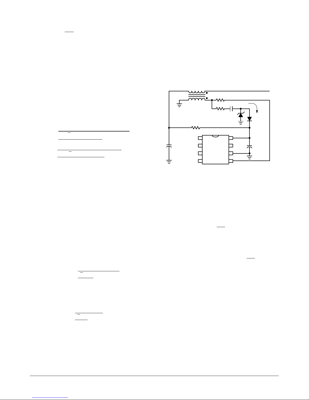
The ZCD winding is a possible solution, but the voltage
induced on the winding may be less than the required
voltage. An alternative is to implement a charge pump to
supply V
Figure 7. The ZCD Winding Supplies V
. A schematic is illustrated in Figure 7.
CC
R
ZCD
C
R
1
D
AUX
R
start
NCP1608
1
+
C
in
2
3
4
FB
Control
Ct
CS
V
CC
DRV
GND
ZCD
8
7
6
5
Charge Pump Circuit
I
3
AUX
D
1
+
C
Vcc
using a
CC
C3 stores the energy for the charge pump. R1 limits the
current by reducing the rate of voltage change. D
AUX
supplies
current to C3 when its cathode is negative. When its cathode
is positive it limits the maximum voltage applied to V
CC
.
The voltage change across C3 over one period is
calculated using Equation 21:
V
DVC3+
The current that charges C
N
out
* V
CC
is calculated using
Vcc
(eq. 21)
Equation 22:
(eq. 22)
V
out
I
+ C3 @ fSW@ DVC3+ C3 @ fSW@
AUX
ǒ
N
* V
CC
Ǔ
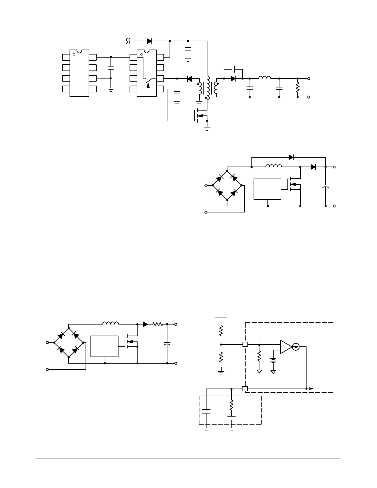
For off−line ac-dc applications that require PFC, a 2-stage
approach is typically used. The first stage is the CrM boost
PFC. This supplies the 2nd stage, which is traditionally an
isolated flyback or forward converter. This solution is
cost−effective and exhibits excellent performance. During
low output power conditions the PFC stage is not required
and reduces efficiency. Advanced controllers, such as the
NCP1230 and NCP1381 detect the low output power
condition and shut down the PFC stage by removing
PFC(V
) (Figure 8).
CC
http://onsemi.com
7
Page 8
1
2
3
4
NCP1608
NCP1608BOOSTGEVB
D
+
C
PFC(VCC)
88
+
7
6
5
1
2
3
4
NCP1230
7
V
CC
6
+
5
Figure 8. Using the SMPS Controller to Supply Power to the NCP1608
bulk
+
+
+
−
DESIGN STEP 8: Limit the Inrush Current
The sudden application of the ac line voltage to the PFC
pre−converter causes an inrush current and a resonant
voltage overshoot that is several times the normal value.
Resizing the power components to handle inrush current and
a resonant voltage overshoot is cost prohibitive.
1. External Inrush Current Limiting Resistor
A NTC (negative temperature coefficient) thermistor
connected in series with the diode limits the inrush current
(Figure 9). The resistance of the NTC decreases from a few
ohms to a few milliohms as the NTC is heated by the I
2
power dissipation. However, an NTC resistor may not be
sufficient to protect the inductor and C
from inrush
bulk
current during a brief interruption of the ac line voltage, such
as during ac line dropout and recovery.
2. Startup Bypass Rectifier
A rectifier is connected from V
in
to V
(Figure 10). This
out
bypasses the inductor and diverts the startup current directly
to C
bulk
. C
is charged to the peak ac line voltage without
bulk
resonant overshoot and without excessive inductor current.
After startup, D
is reverse biased and does not interfere
bypass
with the boost converter.
NTC
+
V
out
Vac
V
in
NCP1608
D
bypass
V
in
+
NCP1608
Vac
V
out
Figure 10. Use a Second Diode to Route the
R
Inrush Current Away from the Inductor
DESIGN STEP 9: Develop the Compensation Network
The pre−converter is compensated to ensure stability over
the input voltage and output power range. To compensate the
loop, a compensation network is connected between the
Control and ground pins. To ensure high PF, the bandwidth
of the loop is set below 20 Hz. A type 2 compensation
network is selected for this design to increase the phase
margin. The type 2 compensation network is shown in
Figure 11.
V
out
R
out1
FB
R
R
out2
FB
E/A
−
+
+
gm
V
REF
Figure 9. Use a NTC to Limit the Inrush Current
Through the Inductor
http://onsemi.com
8
Control
C
COMP
R
COMP1
C
Compensation
Network
COMP1
Figure 11. Type 2 Compensation Network
V
Control
Page 9
NCP1608BOOSTGEVB
The type 2 network is composed of C
R
COMP1
. C
sets the crossover frequency (f
COMP1
COMP
, C
COMP1
CROSS
, and
) and
is calculated using Equation 23:
C
For this design, f
+
COMP1
is set to 5 Hz at the average input
CROSS
gm
2 @ p @ f
CROSS
(eq. 23)
voltage (175 Vac) to decrease THD and gm is specified in the
NCP1608 datasheet:
C
COMP1
+
2 @ p @ 5
110 m
+ 3.5 mF
A normalized value of 3.3 mF is selected, which sets
f
to 5.3 Hz.
CROSS
The addition of R
response. The zero frequency (f
COMP1
causes a zero in the loop
) is typically set to half
zero
the crossover frequency, which is 2.5 Hz for this case.
R
is calculated using Equation 24:
COMP1
L
R
R
R
C
is selected as 20 kW.
COMP1
is used to filter high frequency noise and is set to
COMP
COMP1
COMP1
+
2 @ p @ f
+
2 @ p @ 2.5 @ 3.3 m
between 1/10 and 1/5 of C
selected to be 1/5 of C
C
C
is selected as 0.68 mF.
COMP
COMP
COMP1
ǒ
+
1
5
1
@ C
zero
COMP
1
. For this design, C
COMP1
.
Ǔ
@ 3.3 m + 0.66 mF
+ 19.3 kW
The phase margin and crossover frequency change with
the ac line voltage. It is critical that the gain and phase are
measured for all operating conditions. The measurement
setup using a network analyzer is shown in Figure 12.
Ch A
High−Voltage
(> 450 V)
Isolation Probe
Network Analyzer
Ch B
High−Voltage
(> 450 V)
Isolation Probe
D
(eq. 24)
is
COMP
V
out
R
ZCD
R
out1
in
R
out2
C
COMP
1
2
3
4
Ct
AC Line
EMI
Filter
+
C
Figure 12. Gain-Phase Measurement Setup for a Boost PFC Pre−Converter
There is a tradeoff of transient response for PF and THD.
The low bandwidth of the feedback loop reduces the Control
pin ripple voltage. The reduction of the Control pin ripple
voltage increases PF and reduces THD, but increases the
magnitude of overshoots and undershoots.
Additional THD Reduction
The constant on time architecture of the NCP1608
provides flexibility in optimizing each design.
The following design guidelines provide methods to
further improve PF and THD.
Isolator
1 kW
V
NCP1608
FB
Control
Ct
CS
V
CC
DRV
GND
ZCD
CC
8
7
6
5
M
R
sense
+
C
bulk
1. Improve the THD/PF at Maximum Output Power by
Increasing the On Time at the Zero Crossing:
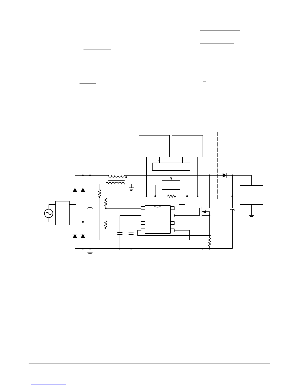
One disadvantage of constant on time CrM control is that
at the zero crossing of the ac line, the instantaneous input
voltage is not large enough to store sufficient energy in the
inductor during the constant on time. Minimal energy is
processed and “zero crossing distortion” is produced as
shown in Figure 13.
Load
http://onsemi.com
9
Page 10
NCP1608BOOSTGEVB
Vin (100V/div)
Iin (500mA/div)
V
(10V/div, ac coupled)
out
Zero
Crossing
Distortion
Figure 13. Full Load Input Current (Vin = 230 Vac 50 Hz, I
The zero crossing distortion increases the THD and
decreases the PF of the pre-converter. To meet
IEC61000-3-2 requirements, this is generally not an issue as
the NCP1608 reduces input current distortion with sufficient
margin. If improved THD or PF is required, then zero
crossing distortion must be reduced. To reduce the zero
crossing distortion, the on time is increased as the
instantaneous input voltage is decreasing to zero. This
increases the time for the inductor current to build up and
V
in
V
in
+
R
CTUP
Ct
AC Line
I
CTUP
+
C
in
R
CTUP
Ct
= 250 mA)
out
reduces the instantaneous input voltage at which the
distortion begins.
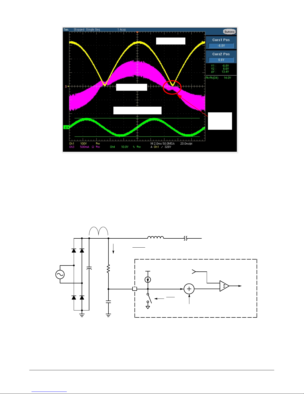
This method is implemented by connecting a resistor from
V
to Ct as shown in Figure 14. The resistor current (I
in
is proportional to the instantaneous line voltage and is
summed with I
I
is maximum at the peak of Vin and is approximately
CTUP
to increase the charging current of Ct.
charge
zero at the zero crossing.
L
V
DD
I
charge
DRV
V
Control
Ct
PWM
−
+
(offset)
)
CTUP
t
on
Figure 14. .Add R
CTUP
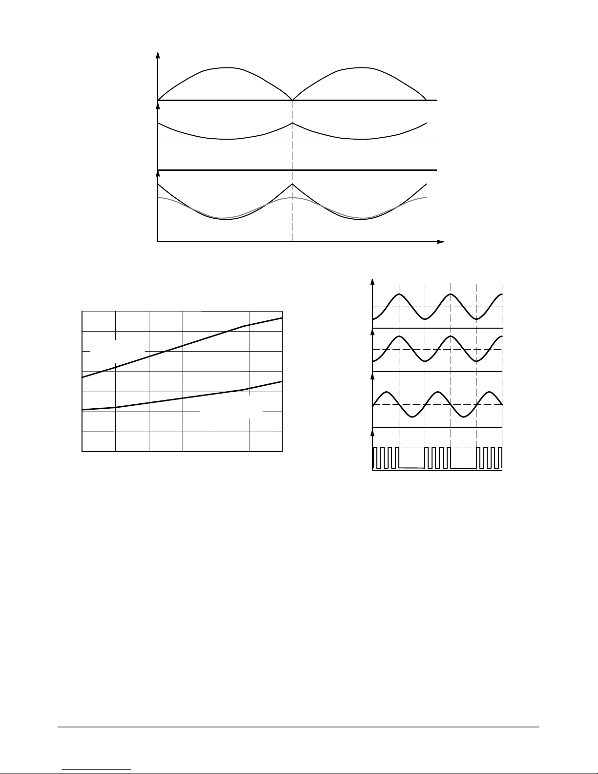
The increased charging current at the peak of Vin enables
the increased sizing of the Ct capacitor without reducing the
control range at Vac
or low output power. The larger value
HL
of the Ct capacitor increases the on time near the zero
crossing and reduces the zero crossing distortion as shown
to Modulate the On Time and Reduce Zero Crossing Distortion
in Figure 15. This reduces the frequency variation over the
ac line cycle. The tradeoff is that the standby power
dissipation is increased by R
. The designer must
CTUP
balance the desired THD and PF performance with the
standby power dissipation requirements.
http://onsemi.com
10
Page 11
Vac(t)
t
f
SW
NCP1608BOOSTGEVB
with R
CTUP
on
no R
CTUP
no R
CTUP
with R
CTUP
time
Figure 15. On Time and Switching Frequency With and Without R
The dependency of THD on R
is illustrated in
CTUP
Figure 16.
14
12
R
= open
CTUP
10
Ct = 1 nF
8
6
THD (%)
4
2
0
85 115 145 175 205 235 265
Vin (Vac)
Figure 16. Dependency of THD on R
(I
= 250 mA)
out
R
= 1.5 MW
CTUP
Ct = 1.22 nF
CTUP
2. Improve the THD/PF at Maximum Input Voltage or
Low Output Current:
If the required on time at maximum input voltage or low
output current is less than the minimum on time (t
PWM
), then
DRV pulses must be skipped to prevent excessive power
delivery to the output. This results in the following
sequence:
1. The excessive on time causes V
to Ct
2. When V
3. The drive is disabled and V
4. As V
.
(offset)
Control
decreases, V
out
< Ct
, the drive is disabled.
(offset)
out
increases.
Control
decreases.
Control
to decrease
5. The sequence repeats. Figure 17 depicts the
sequence:
CTUP
V
out
V
out
V
FB
V
REF
V
Control
Ct
(offset)
DRV
Figure 17. Required On Time Less Than the
Minimum On Time
This sequence increases the input current distortion.
There are two solutions to improve THD/PF at maximum
input voltage or low output current:
1. Properly size the Ct capacitor. As previously
mentioned, the Ct capacitor is sized to set the
maximum on time for minimum line input voltage
and maximum output power. Sizing Ct to an
excessively large value reduces the control range
at Vac
or low output power.
HL
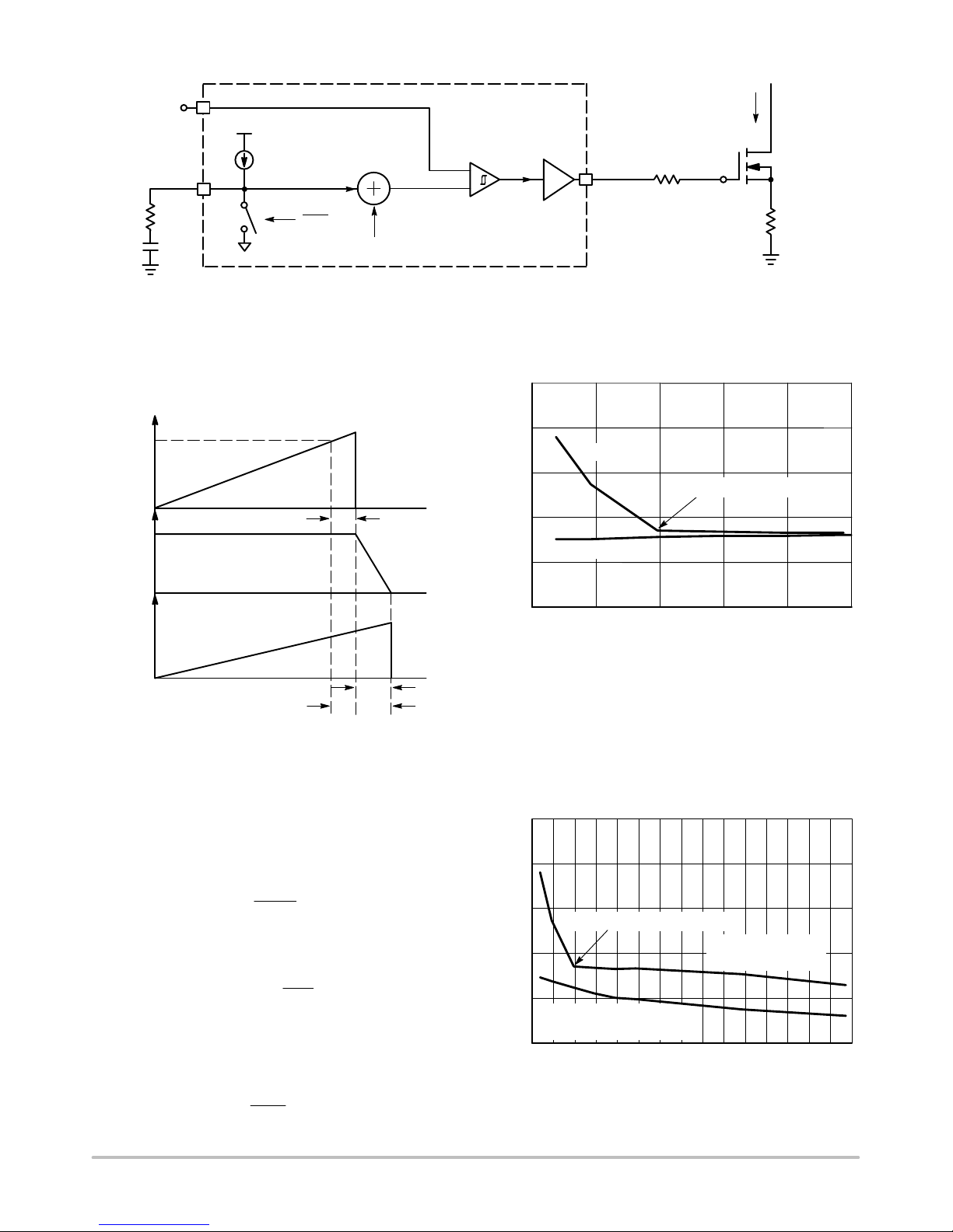
2. Compensate for propagation delays. If optimizing
the Ct capacitor does not achieve the desired
performance, then it may be necessary to
compensate for the PWM propagation delay by
connecting a resistor (R
When the Ct voltage reaches the V
) in series with Ct.
CT
Control
setpoint,
the PWM comparator sends a signal to end the on
time of the driver as shown in Figure 18.
http://onsemi.com
11
Page 12
Control
R
Ct
CT
NCP1608BOOSTGEVB
V
Control
V
DD
Driver
DRV
V
gate
R
DRV
V
PWM
−
+
Ct(off)
I
Ct
charge
DRV
Ct
(offset)
Figure 18. Block Diagram of the Propagation Delay Components
I
switch
R
sense
There is a delay (t
when the MOSFET completely turns off. t
the propagation delay of the PWM comparator (t
) from when V
delay
is reached to
Ct(off)
delay
is caused by
) and
PWM
the time for the gate voltage of the MOSFET to decrease to
zero (t
). The delays are illustrated in Figure 19.
gate
V
Ct(off)
Ct
V
gate
I
switch
Figure 19. Turn Off Propagation Delays
t
PWM
t
gate
t
delay
The total delay is calculated using Equation 25:
t
+ t
delay
t
increases the effective on time of the MOSFET.
delay
If a resistor (R
) is connected in series with the Ct
CT
PWM
) t
gate
(eq. 25)
capacitor, then the total on time reduction is calculated using
Equation 26:
DV
Dton+ Ct @
DI
RCT
RCT
+ Ct @ R
CT
(eq. 26)
The value of RCT to compensate for the propagation delay
is calculated using Equation 27:
t
RCT+
delay
Ct
The NCP1608 datasheet specifies the maximum t
130 ns. t
MOSFET and R
is a dependent on the gate charge of the
gate
. For this demo board, the gate delay is
DRV
(eq. 27)
PWM
as
measured as 230 ns.
360 n
RCT+
1n
+ 360 W
A value of RCT = 365 W compensates for the propagation
delays. Figure 20 shows the decrease of THD at Vac
HL
and
low output power by compensating for the propagation delay.
50
40
RCT = 0 W
30
THD (%)
20
10
RCT = 365 W
0
25 30 35 40 45 50
DRV Pulse Skipping Begins
P
(W)
out
Figure 20. Low Output Power THD Reduction with
R
(Vin = 265 Vac 50 Hz, R
CT
= open, Ct = 1 nF)
CTUP
Both THD reduction techniques can be combined to
decrease the THD for the entire output power range.
Figure 21 shows the decreased THD at the maximum input
voltage
across the output power range by decreasing zero
crossing distortion and by compensating for the propagation
delay.
50
40
30
THD (%)
20
10
0
Figure 21. THD Reduction with R
DRV Pulse Skipping Begins
R
= open
CTUP
R
= 0 W Ct = 1 nF
CT
R
= 1.5 MW
CTUP
R
= 365 W Ct = 1.22 nF
CT
P
out
65 75
(W)
CTUP
and R
CT
25 35 45 55 85 95
(Vin = 265 Vac 50 Hz)
http://onsemi.com
12
Page 13
NCP1608BOOSTGEVB
Design Results
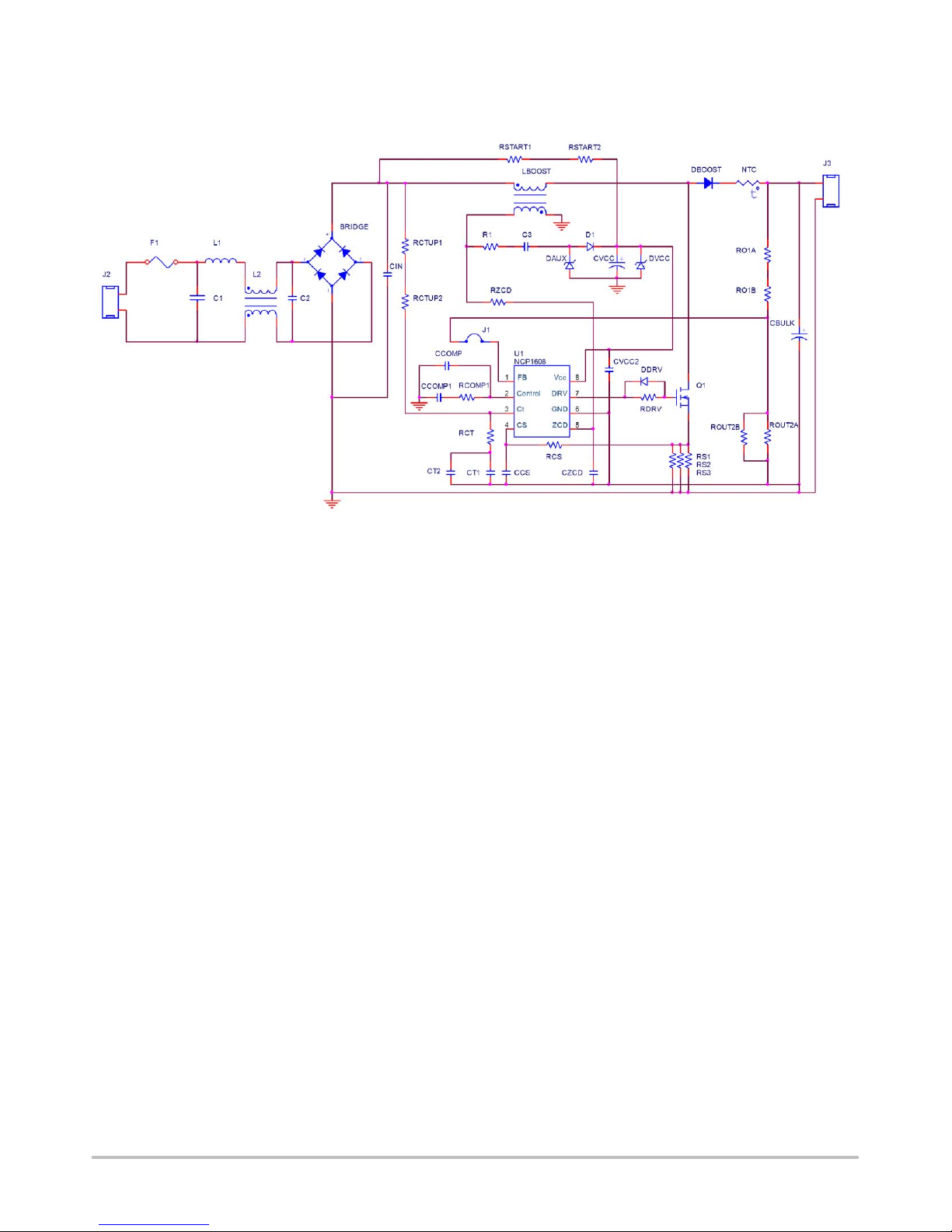
The completed evaluation board schematic is shown in Figure 22.
Figure 22. NCP1608BOOSTGEVB Evaluation Board Schematic
The bill of materials (BOM), layout, and summary of
boost equations are shown in Appendix 1, Appendix 2, and
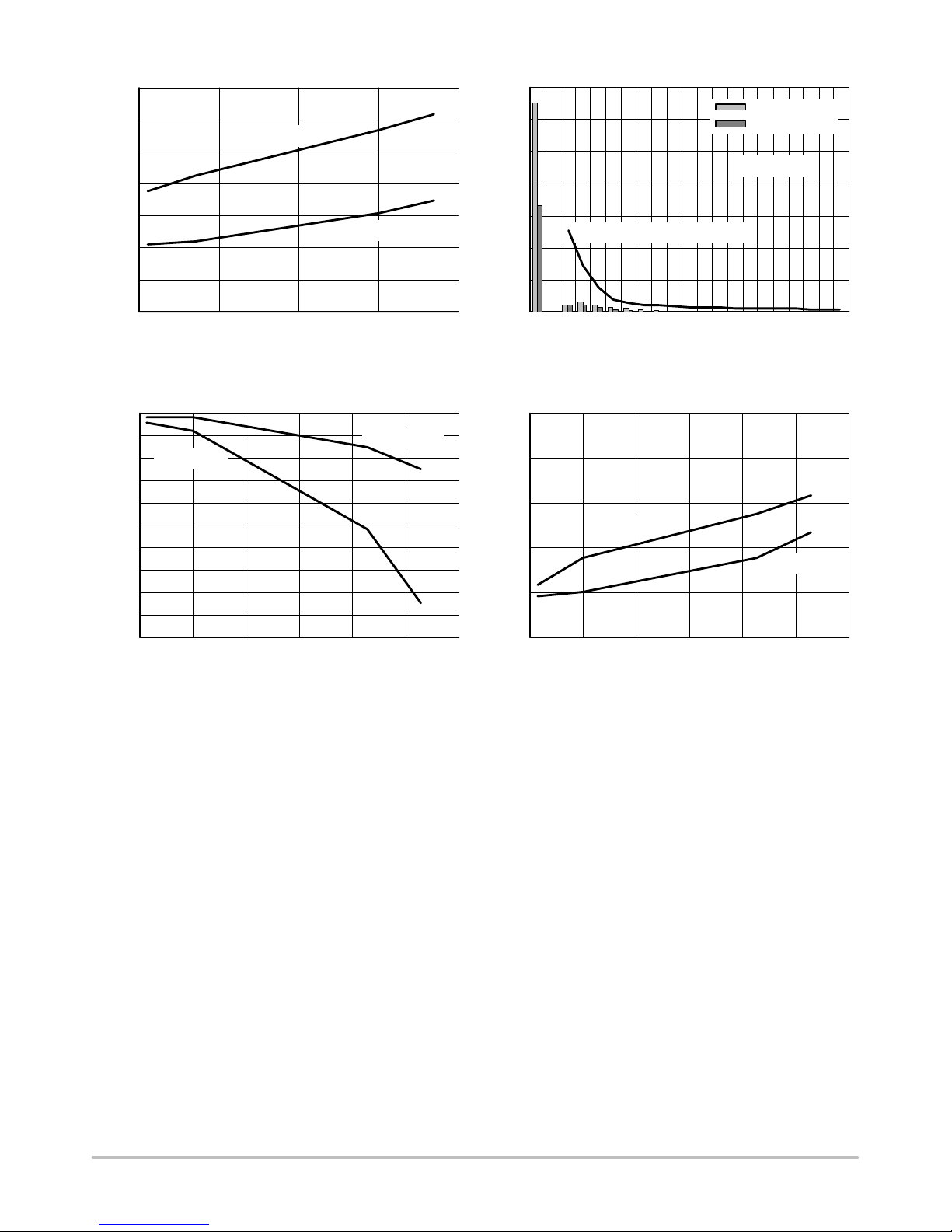
Appendix 3 respectively. This pre−converter exhibits
excellent THD (Figure 23 and Figure 24), PF (Figure 25),
and efficiency (Figure 26). All measurements are performed
with the following conditions:
− After the board is operated at full load and minimum line
input voltage for 30 minutes
− At an ambient temperature of 25°C, open frame, and
without forced air flow
− The input power, PF, and THD are measured using a
PM3000A power meter
− The output voltage is measured using a HP34401A
multimeter
− The output current is set using a PLZ1003WH electronic
load
− The output current is measured using a HP34401A
multimeter
− The output power is calculated by multiplying the output
voltage and output current
http://onsemi.com
13
Page 14
NCP1608BOOSTGEVB
14
12
10
8
6
THD (%)
4
2
0
1.00
0.99
0.98
0.97
0.96
0.95
PF
0.94
0.93
0.92
0.91
0.90
0.7
0.6
P
= 50 W
out
0.5
0.4
0.3
P
= 100 W
out
IEC61000−3−2 Class D Limits
0.2
HARMONIC CURRENT (A)
0.1
0
28023018013080
21 33 37
Vin (Vac) Nth HARMONIC
Figure 23. THD vs. Input Voltage Figure 24. Individual Harmonic Current
100
P
= 100 W
out
P
= 50 W
out
98
96
P
= 100 W
out
94
EFFICIENCY (%)
92
90
29025522018515011580
Vin (Vac) Vin (Vac)
Figure 25. PF vs. Input Voltage Figure 26. Efficiency vs. Input Voltage
115 Vac 60 Hz
230 Vac 50 Hz
Pin = 75 W
29251713951
312719151173233539
P
= 50 W
out
29025522018515011580
http://onsemi.com
14
Page 15
NCP1608BOOSTGEVB
Input Current and Output Voltage
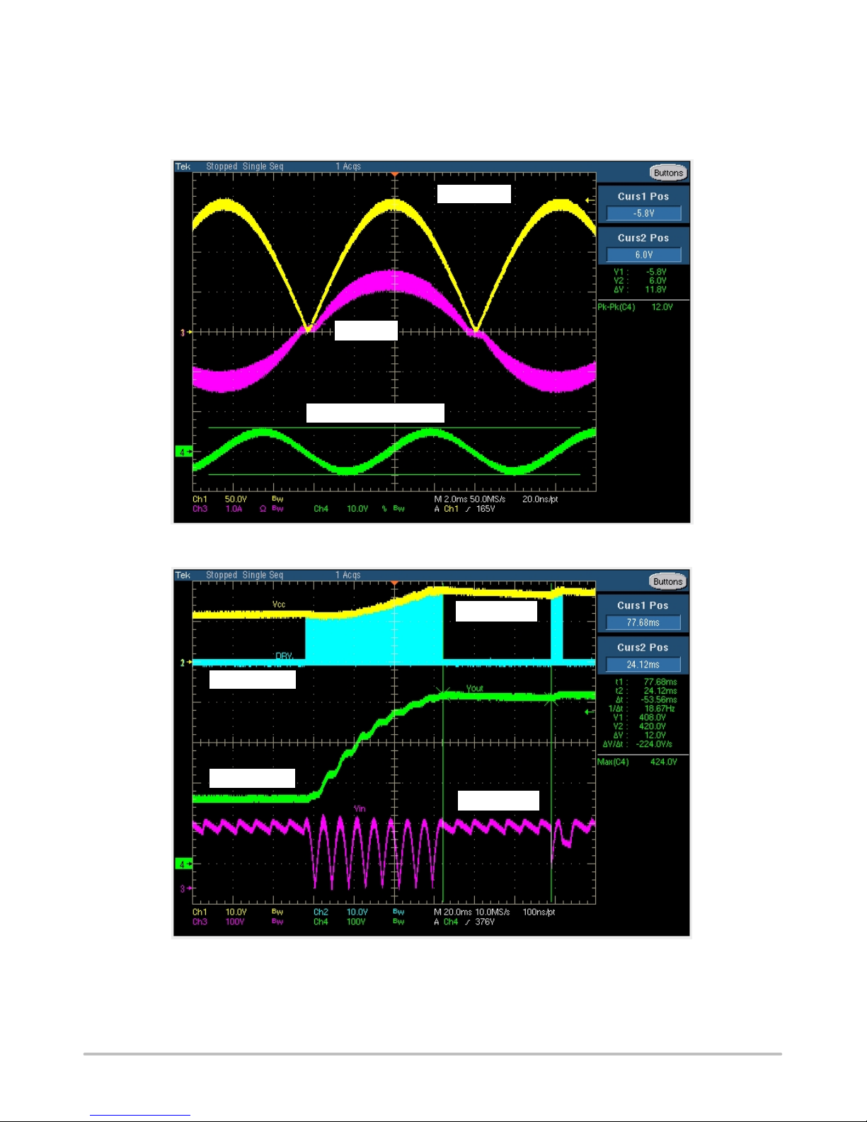
The input current and output voltage ripple are shown in
Figure 27. The overvoltage protection is observed by
starting up the pre-converter with no load as shown in
Iin (1A/div)
V
(10V/div, ac coupled)
out
Figure 28. The NCP1608 detects an OVP fault when V
reaches 421 V and restarts when V
Vin (50V/div)
decreases to 410 V.
out
out
Figure 27. Input Current and Output Voltage Ripple (Vin = 115 Vac 60 Hz, I
VCC (10V/div)
V
(10V/div)
DRV
V
(100V/div)
out
Vin (100V/div)
= 250 mA)
out
Figure 28. Startup Transient Showing OVP Detection and Recovery (Vin = 115 Vac 60 Hz, I
http://onsemi.com
15
= 0 mA)
out
Page 16
NCP1608BOOSTGEVB
Frequency Response
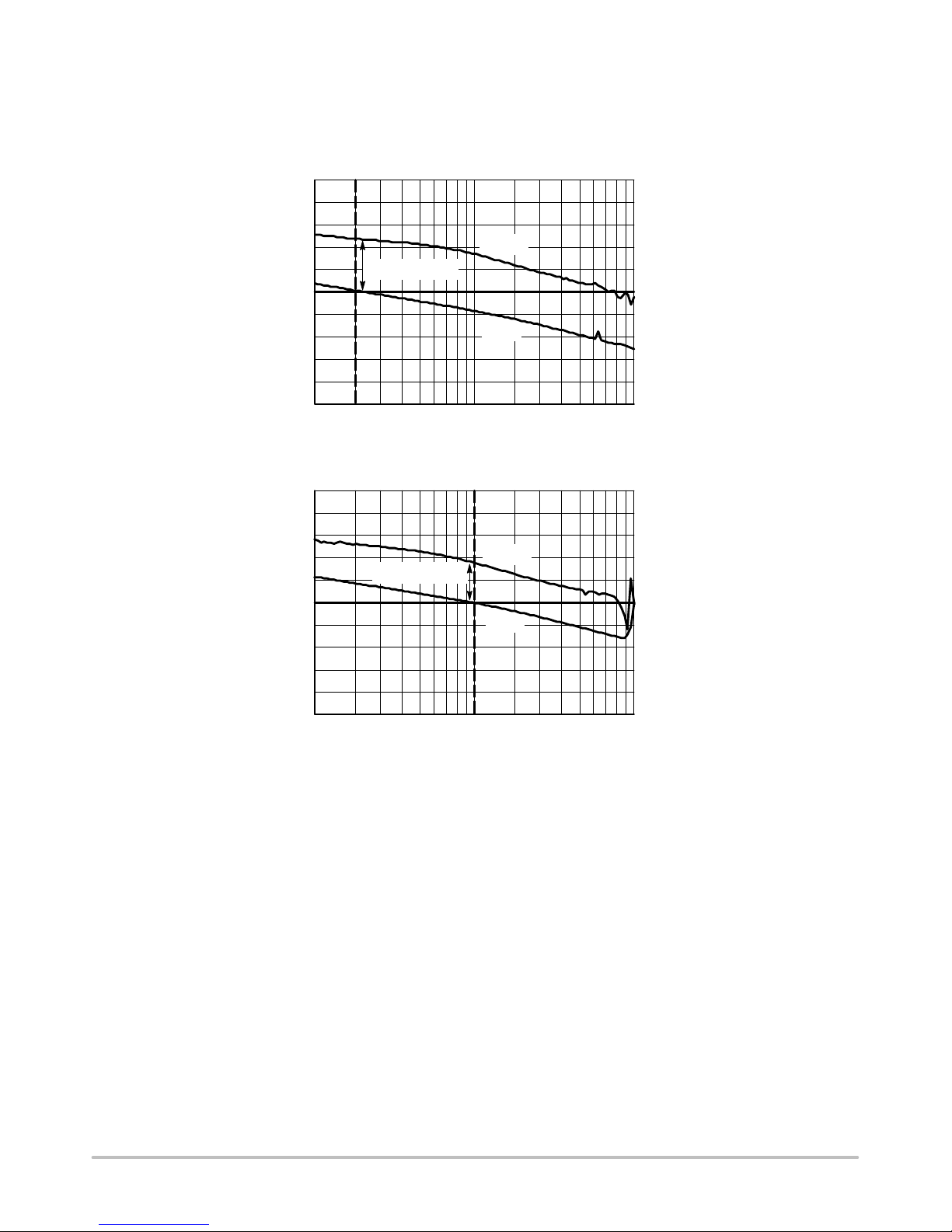
The frequency response is measured at the minimum and
maximum input voltages and maximum output power.
Figure 29 shows that at minimum input voltage, the
crossover frequency is 2 Hz and the phase margin is 71°.
Figure 30 shows that at maximum input voltage, the
crossover frequency is 10 Hz and the phase margin is 53°.
100
80
60
40
20
0
−20
GAIN (dB)
−40
−60
−80
−100
1 10 100
Phase Margin
f
CROSS
FREQUENCY (Hz)
Phase
Gain
Figure 29. Frequency Response Vin = 85 Vac 60 Hz I
100
80
60
10
f
CROSS
Phase
Gain
40
20
0
−20
GAIN (dB)
−40
−60
−80
−100
1 100
Phase Margin
FREQUENCY (Hz)
Figure 30. Frequency Response Vin = 265 Vac 50 Hz I
= 250 mA
out
= 250 mA
out
150
120
90
60
30
0
−30
PHASE (degrees)
−60
−90
−120
−150
150
120
90
60
30
0
−30
PHASE (degrees)
−60
−90
−120
−150
http://onsemi.com
16
Page 17
NCP1608BOOSTGEVB
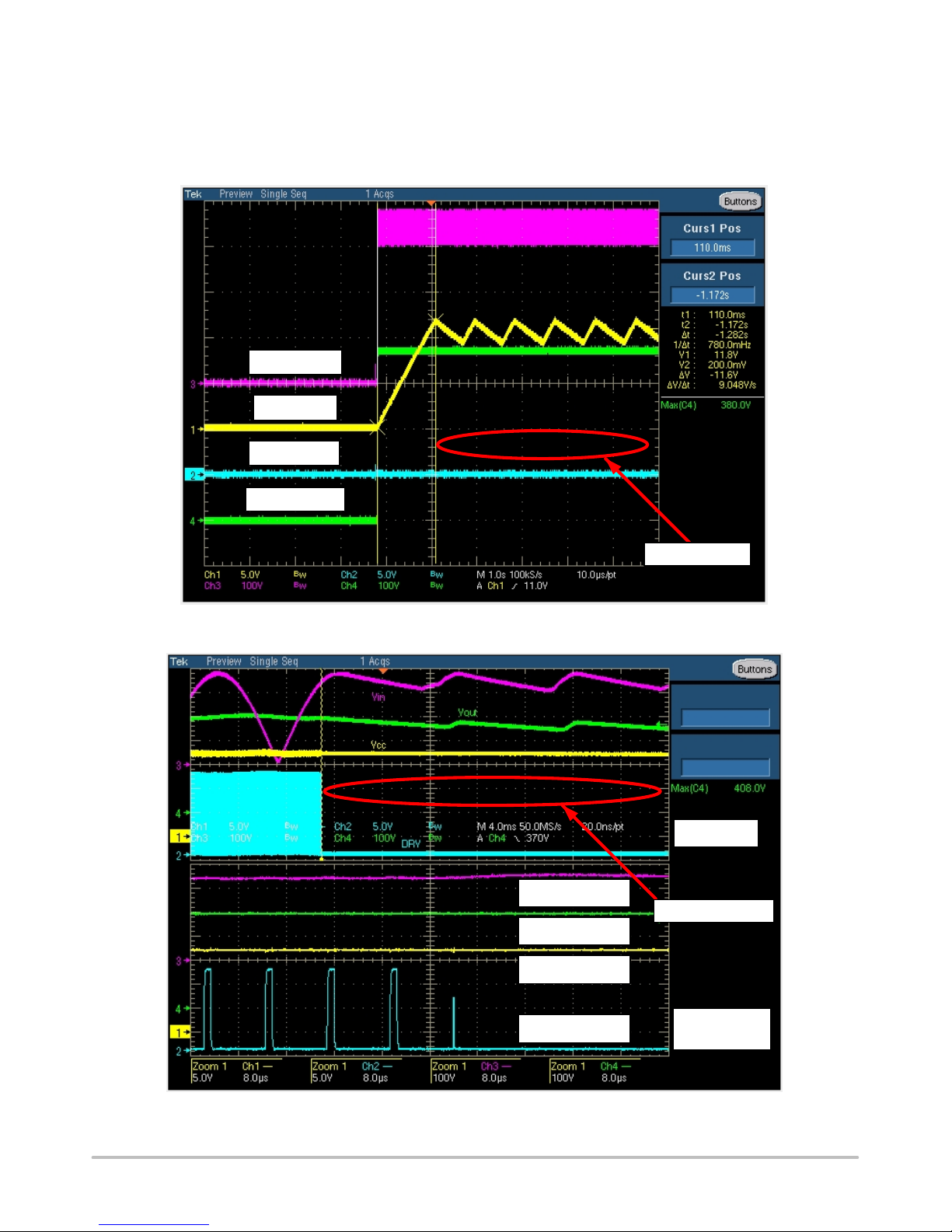
Floating Pin Protection (FPP) Jumper
The evaluation board includes a jumper (J1) between the
FB pin and the feedback network to demonstrate the FPP
feature of the NCP1608. If J1 is removed before applying the
line input voltage, the drive is never enabled as shown in
Vin (100V/div)
VCC (5V/div)
V
(5V/div)
DRV
V
(100V/div)
out
Figure 31. If J1 is removed during operation, the drive is
disabled as shown in Figure 32. J1 is for FPP evaluation
purposes only and should not be included in manufactured
systems.
Figure 31. Startup with Jumper Removed (Vin = 265 Vac 50 Hz, I
Vin (100V/div)
V
(100V/div)
out
VCC (5V/div)
No DRV Pulses
= 0 mA)
out
t(4ms/div)
DRV Pulses Stop
Figure 32. Removing the Jumper During Operation (Vin = 265 Vac 50 Hz, I
http://onsemi.com
17
V
DRV
(5V/div)
t(8μs/div)
(Zoomed In)
= 250 mA)
out
Page 18

NCP1608BOOSTGEVB
The evaluation board can be configured for THD reduction or power dissipation reduction. Table 3 shows the configuration
results.
Table 3. EVALUATION BOARD CONFIGURATION RESULTS
Efficiency (P
Ct
(R
R
CTUP
open 1 nF 224 mW 93.5% 95.7% 8.4% 12.5%
1.5 MW
= 0 W)
CT
1.22 nF 294 mW 93.5% 95.5% 4.4% 6.2%
Shutdown Power Dissipation (VFB = 0 V)
(V
= 265 Vac 50 Hz)
in
115 Vac
60 Hz
= 100 W) THD (P
out
230 Vac
50 Hz
115 Vac
60 Hz
= 100 W)
out
230 Vac
50 Hz
Safety Precautions
Since the FPP feature is only intended to protect the
system in the case of a floating FB pin, care must be taken
when removing the jumper. Do not attach any wires to the
jumper pins with the jumper removed. Connecting wires
to the FB pin couples excessive noise to the FB pin. This
prevents the correct operation of FPP and causes maximum
power to be delivered to the output. This can cause excessive
voltage to be applied to C
. Always wear proper eye
bulk
protection when the jumper is removed.
The jumper is located next to high voltage components.
Do not remove the jumper during operation with bare
fingers or non-insulated metal tools.
Layout Considerations
Careful consideration must be given to the placement of
components during layout of switching power supplies.
Noise generated by the large voltages and currents can be
coupled to the pins of the NCP1608. The following
guidelines reduce the probability of excessive coupling:
1. Place the following components as close as
possible to the NCP1608:
a. Ct capacitor
b. V
decoupling capacitor
CC
c. Control pin compensation components
2. Minimize trace length, especially for high current
loops.
3. Use wide traces for high current connections.
4. Use a single point ground connection between
power ground and signal ground.
The evaluation board includes the following unpopulated
footprints to enable user experimentation:
1. CCS to add a decoupling capacitor to the CS pin.
2. CZCD to add a decoupling capacitor to the ZCD
pin.
3. DDRV to add a diode for faster turn off of Q1.
4. DVCC to add a diode to clamp V
CC
.
5. ROUT2B to add a resistor for a more accurate
output voltage.
6. RS3 to add a resistor for a more accurate inductor
peak current limit or to reduce the heating of the
current sense resistors.
Summary
A universal input voltage 100 W converter is designed
using the boost topology. The converter is implemented with
the NCP1608. Over the input voltage range and with an
output power of 100 W, the PF, THD, and efficiency are
measured as greater than 0.97, less than 8%, and greater than
92% respectively. The converter complies with
IEC61000−3−2 Class D limits for an input power of 75 W.
The converter is stable over the input voltage range with a
measured phase margin greater than 50 degrees. Finally, the
overvoltage protection and floating pin protection features
protect the converter from excessive output voltage.
The evaluation board is designed to showcase the features
and flexibility of the NCP1608. This design is a guideline
only and does not guarantee performance for any
manufacturing or production purposes.
http://onsemi.com
18
Page 19

NCP1608BOOSTGEVB
Table 4. BILL OF MATERIALS*
Desig-
nator
BRIDGE 1 Bridge Rectifier, 4 A, 600 V − − KBL Vishay KBL06-E4/51 Yes
C1, C2 2 Capacitor, EMI Suppression,
C3 1 Capacitor, Ceramic, SMD,
CBULK 1 Capacitor, Electrolytic, 450 V
CCOMP 1 Capacitor, Ceramic, SMD,
CCOMP1 1 Capacitor, Ceramic, SMD,
CCS,
CZCD
CIN 1 Capacitor, EMI Suppression,
CT1 1 Capacitor, Ceramic, SMD,
CT2 1 Capacitor, Ceramic, SMD,
CVCC 1 Capacitor, Electrolytic, 25 V
CVCC2 1 Capacitor, Ceramic, SMD,
D1 1 Diode, Switching, 100 V − − SOD123 ON
DAUX 1 Diode, Zener, 18 V − − SOD123 ON
DBOOST 1 Diode, Ultrafast, 4 A, 600 V − − Axial ON
DDRV 1 Diode, Switching open − SOD123 − − −
DVCC 1 Diode, Zener open − SOD123 − − −
F1 1 Fuse, SMD, 2 A, 600 V − − SMD Littelfuse 0461002.ER Ye s
J1 1 Header 1 Row of 2, 100 mil − − 2.54 mm 3M 929400-01-36-RK Ye s
J2, J3 2 Connector, 156 mil 3 pin − − 156 mil MOLEX 26−60−4030 Ye s
L1 1 Inductor, Radial, 4 A
L2 1 Line Filter, 2.7 A 4.7 mH − Through
LBOOST 1 Inductor, NB:NZCD = 10:1
MECHA−
NICAL
MECHA−
NICAL
MECHA−
NICAL
MECHA−
NICAL
MECHA−
NICAL
MECHA−
NICAL
MECHA−
NICAL
MECHA−
NICAL
Qty Description Value
305 Vac
50 V
25 V
25 V
2 Capacitor, Ceramic, SMD open − 1206 − − −
305 Vac
50 V
50 V
50 V
1 Shorting Jumper on J1 − − − 3M 929955-06 Ye s
1 Heatsink − − TO−220 Aavid 590302B03600 Yes
1
Screw, Phillips, 4−40, ¼”,
1 Nut, Hex 4−40, Steel − − − Building
1 Shoulder Washer #4, Nylon − − − Keystone 3049 Ye s
1 TO 220 Thermal Pad, 9 mil − − − Wakefield 173-9-240P Yes
4 Standoffs, Hex 4−40, 0.75”,
4 Nut, Hex 4−40, Nylon − − − Building
Steel
Nylon
0.47 mF
8.2 nF 5% 1206 TDK
68 mF
0.68 mF
3.3 mF
0.1 mF
1 nF 10% 1206 Yageo CC1206KRX7R9BB102 Yes
220 pF 10% 1206 Yageo CC1206KRX7R9BB221 Ye s
47 mF
0.1 mF
180 mH
400 mH
− − − Building
− − − Keystone 4804K Yes
Toler-
ance
20% Radial EPCOS B32923C3474M Yes
20% Radial United
10% 1206 TDK
10% 1206 TDK
20% Radial EPCOS B32921A2104M Yes
20% Radial Panasonic EEU-FC1E470 Yes
10% 1206 Yageo CC1206KRX7R9BB104 Ye s
10% Radial Coilcraft PCV-2-184-05L No
Footprint Manufacturer
Corporation
Chemi−Con
Corporation
Corporation
Semiconductor
Semiconductor
Semiconductor
Hole
− Custom Coilcraft JA4224−AL No
Panasonic ELF-20N027A Ye s
Fasteners
Fasteners
Fasteners
Manufacturer Part
Number
C3216C0G1H822J Yes
EKXG451ELL680MMN3S Ye s
C3216X7R1E684K Yes
C3216X7R1E335K Yes
MMSD4148T1G No
MMSZ4705T1G No
MUR460RLG No
PMSSS 440 0025 PH Yes
HNSS440 Yes
NY HN 440 Yes
*All products listed are Pb−free
Substi-
tution
Allowed
http://onsemi.com
19
Page 20
NCP1608BOOSTGEVB
Table 4. BILL OF MATERIALS*
Desig-
nator
NTC 1 Thermistor, Inrush Current
Q1 1 MOSFET, N−Channel,
R1 1 Resistor, SMD
RCOMP1 1 Resistor, SMD
RCS 1 Resistor, 0.25 W Axial
RCT 1 Resistor, SMD
RCTUP1,
RCTUP2
RDRV 1 Resistor, SMD
RO1A,
RO1B
ROUT2A 1 Resistor, SMD
ROUT2B 1 Resistor, SMD open − 1206 − − -
RS1, RS2 2 Resistor, SMD, 1 W
RS3 1 Resistor, SMD open − 2512 − − -
RSTART1
RSTART2
RZCD 1 Resistor, 0.25 W Axial
U1 1 CrM PFC Controller NCP1608 − SOIC−8 ON
2 Resistor, 0.25 W Axial
2 Resistor, SMD
2 Resistor, 0.25 W Axial
Limiter
11.6 A, 560 V
4.7 W
− − TO−220 Infineon SPP12N50C3 Yes
100 W
20 kW
510 W
0 W
750 kW
10 W
2 MW
25.5 kW
0.25 W
330 kW
100 kW
Toler-
anceValueDescriptionQty
20% Radial EPCOS B57238S479M Yes
1% 1206 Vishay CRCW1206100RFKEA Ye s
1% 1206 Vishay CRCW120620K0FKEA Yes
5% Axial Yageo CFR-25JB-510R Yes
− 1206 Vishay CRCW12060000Z0EA Yes
5% Axial Yageo CFR-25JB-750K Ye s
1% 1206 Vishay CRCW120610R0FKEA Ye s
1% 1206 Vishay CRCW12062M00FKEA Yes
1% 1206 Vishay CRCW120625K5FKEA Yes
1% 2512 Vishay WSL2512R2500FEA Yes
5% Axial Yageo CFR-25JB-330K Ye s
5% Axial Yageo CFR-25JB-100K Ye s
Semiconductor
Manufacturer Part
NumberManufacturerFootprint
NCP1608BDR2G No
*All products listed are Pb−free
Substi-
tution
Allowed
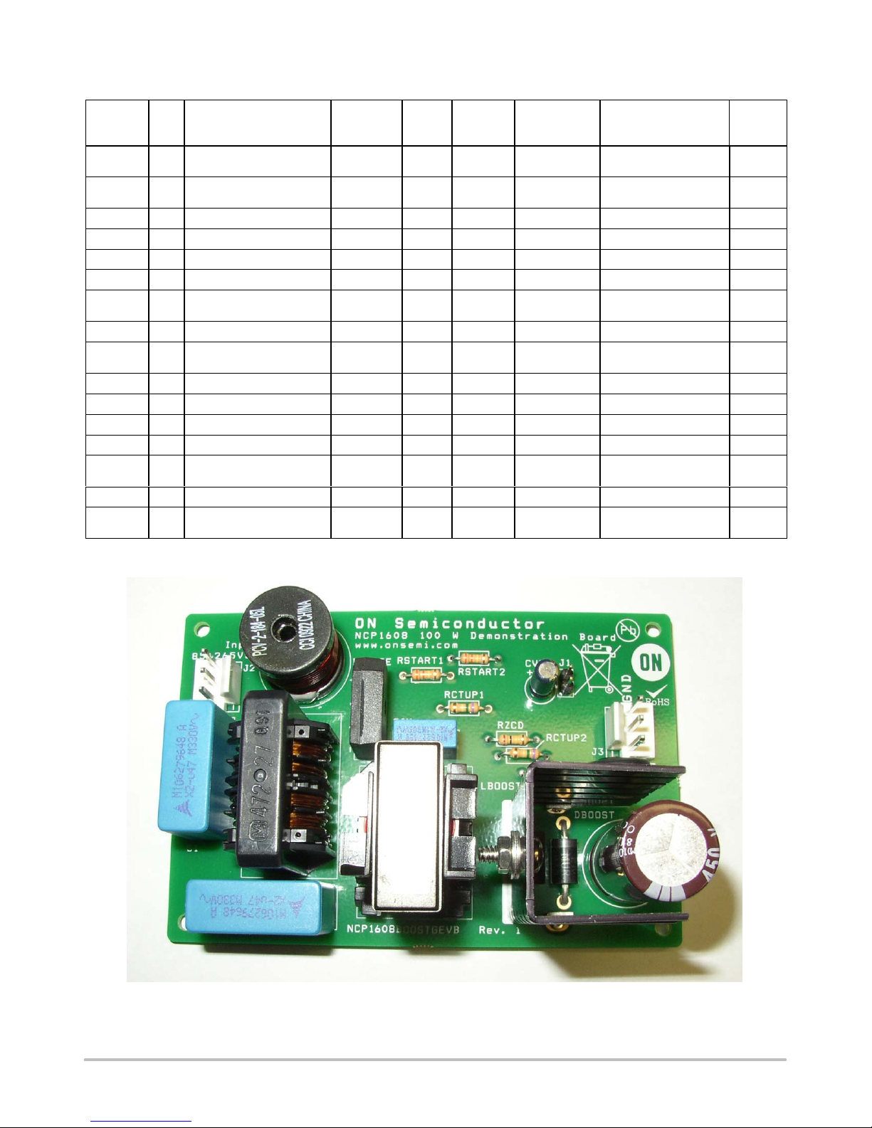
Figure 33. Evaluation Board Photo
http://onsemi.com
20
Page 21
NCP1608BOOSTGEVB
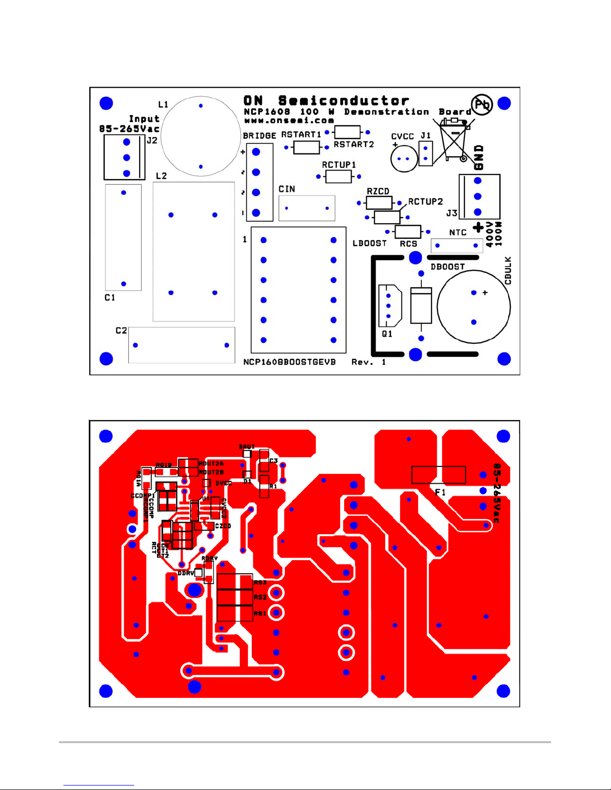
LAYOUT
Figure 34. Top View of the Layout
Figure 35. Bottom View of the Layout
http://onsemi.com
21
Page 22

NCP1608BOOSTGEVB
TEST PROCEDURE FOR THE NCP1608BOOSTGEVB EVALUATION BOARD
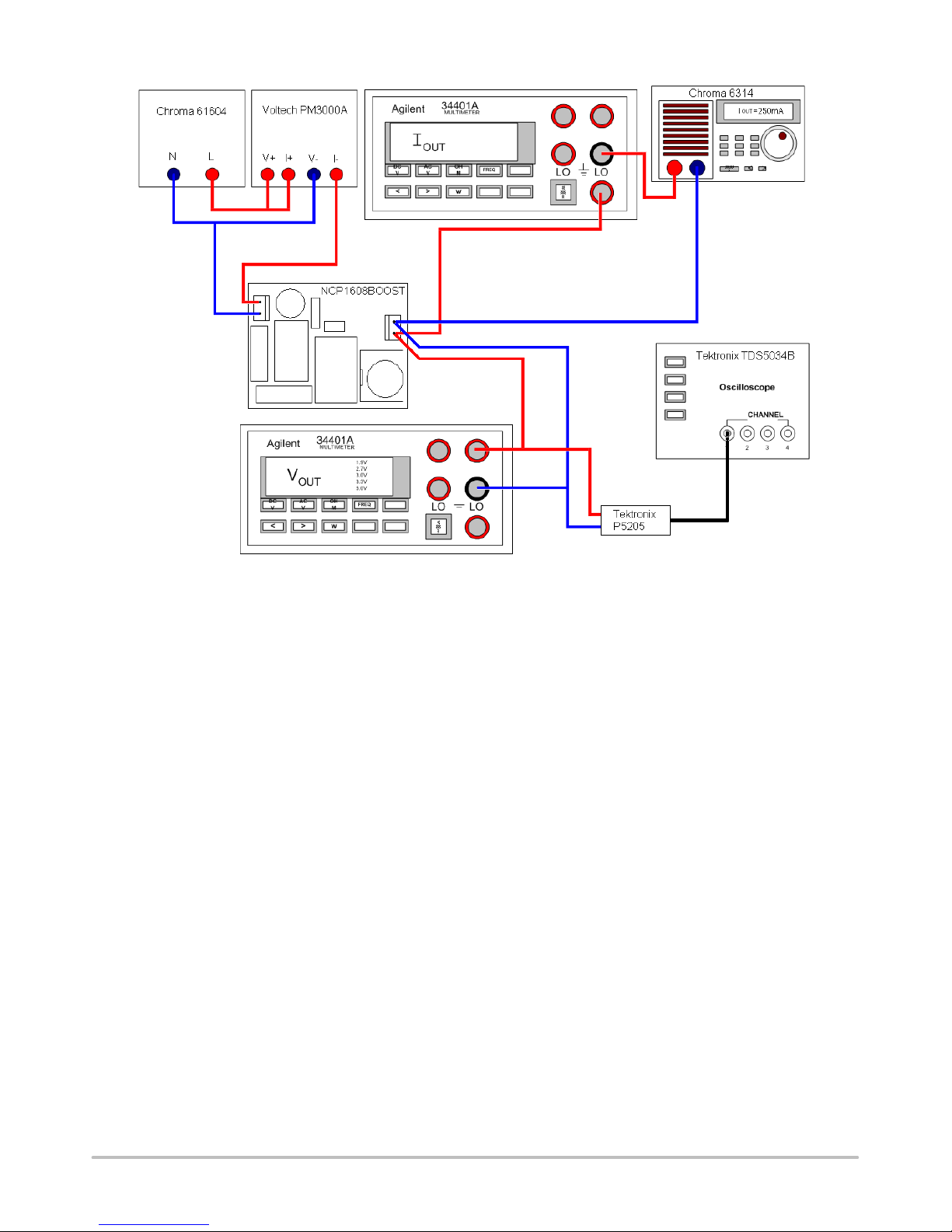
Required Equipment
(*Equivalent test equipment may be substituted.)
• *Chroma 61604 AC Power Source
• *Voltech PM3000A Power Analyzer
• 2× *Agilent 34401A Multimeter
• *Chroma 6314 Electronic Load with *Chroma 63108
High Voltage Module
• *Tektronix TDS5034B Oscilloscope with
*Tektronix P5205 Differential Probes
Test Procedure
1. Ensure that there is a jumper on J1. If not, place a
jumper on J1 for the remainder of the test
procedure.
2. Connect the electronic load with high voltage
module to the output labeled “400 V, 100 W”.
3. Connect one of the multimeters in series with the
output and load and set it to measure current.
4. Connect the second multimeter to the output and
set it to measure voltage.
5. Connect the oscilloscope with differential probes
to the output and set it to measure output ripple
and frequency.
6. Connect the ac power source and power analyzer
to the terminals labeled “Input”. Set the current
compliance limit to 1.8 A.
7. Set the ac power source to 85 Vac / 60 Hz.
8. Set the high voltage electronic load to 250 mA.
9. Turn the AC source on.
10. Wait 10 seconds, and then check the output
voltage (V
multimeter. Verify it is within the limits of
Table 5.
11. Measure power factor (PF) and input power (P
using the power analyzer.
12. Measure the peak-to-peak voltage and frequency
of the output ripple using the oscilloscope.
13. Measure I
14. Calculate efficiency (h) using the equation:
) using the corresponding
OUT
using the corresponding multimeter.
OUT
I
V
h +
OUT
OUT
IN
100%
P
IN
15. Repeat steps 9-13 with the ac source set to 115 Vac
/ 60 Hz, 230 Vac / 50 Hz, 265 Vac / 50 Hz. Verify
the results are within the limits of Table 5.
16. Turn off the ac source.
17. Since high voltage will be present after the voltage
is removed, wait for the dc voltmeter to show
approximately 0 V before continuing.
18. Disconnect the ac source.
19. Disconnect the oscilloscope.
20. Disconnect the electronic load.
21. Disconnect both multimeters.
22. End of test.
Table 5. DESIRED RESULTS
For 85 Vac /
60 Hz input
For 115 Vac /
60 Hz input
For 230 Vac /
50 Hz input
)
For 265 Vac /
50 Hz input
V
= 397 ±15 V
OUT
PF > 0.99
Output Ripple Voltage < 20 V
Output Ripple Frequency = 120 Hz sine
wave
h > 90%
V
= 397 ±15 V
OUT
PF > 0.99
Output Ripple Voltage < 20 V
Output Ripple Frequency = 120 Hz sine
wave
h > 90%
V
= 397 ±15 V
OUT
PF > 0.95
Output Ripple Voltage < 20 V
Output Ripple Frequency = 100 Hz sine
wave
h > 90%
V
= 397 ±15 V
OUT
PF > 0.95
Output Ripple Voltage < 20 V
Output Ripple Frequency = 100 Hz sine
wave
h > 90%
PP
PP
PP
PP
http://onsemi.com
22
Page 23
NCP1608BOOSTGEVB
Figure 36. Test Setup
http://onsemi.com
23
Page 24
NCP1608BOOSTGEVB
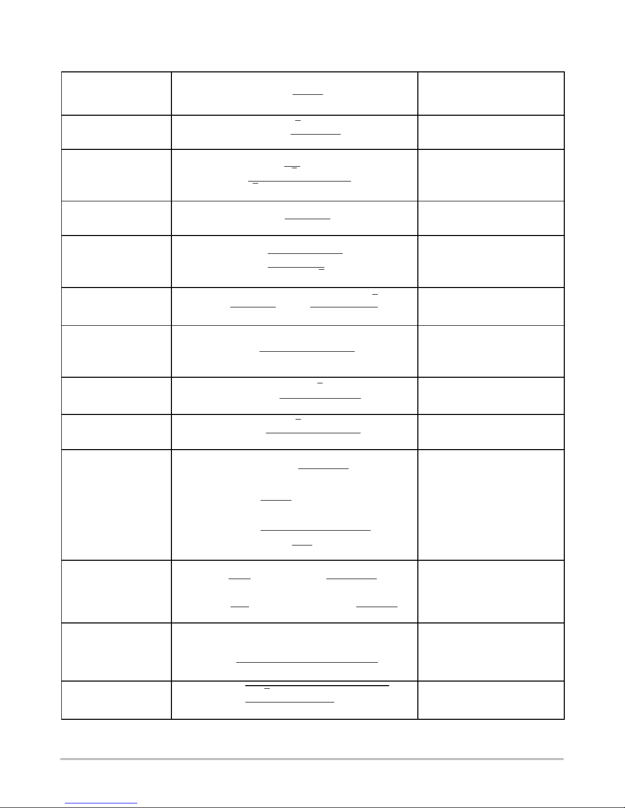
Table 6. SUMMARY OF BOOST EQUATIONS Components are identified in Figure 3
Input rms Current
Inductor Peak Current
Inductor Value
On Time
Off Time
Switching Frequency
On Time Capacitor
Inductor Turns to ZCD
Turns Ratio
Resistor from ZCD
Winding to the ZCD pin
Output Voltage and
Output Divider
Output Voltage OVP
Detection and Recovery
Output Voltage Ripple and
Output Capacitor Value
Output Capacitor rms
Current
V
out(OVP)
V
out(OVPL)
I
fSW+
V
out
C
C(RMS)
+
bulk
I
L(peak)
Vac2@
L v
Ǹ
2
t
+
off
2
Vac
2 @ L @ P
Ct w
NB:N
ZCD
R
w
ZCD
+ V
+
ǒ
V
ripple(peak−peak)
+
@ǒR
REF
R
+
out1
R
+
out2
V
OVP
@ V
V
REF
V
OVP
ǒ
@ V
V
REF
w
2 @ p @ V
Ǹ
9 @ p @ Vac @ V
Iac +
@ V
ton+
Vac@ŤsinqŤ@ 2
@ h
out
2 @ P
h @ Vac
v
I
V
I
bias(out)
RFB@
REF
REF
Ǹ
2
P
out
h @ Vac
Ǹ
@ 2 @ P
2
+
h @ Vac
V
out
ǒ
* VacǓ@ h
Ǹ
2
@ P
out
@ f
out
2 @ L @ P
h @ Vac
t
on
V
out
Ǹ
@ L
out
LL
V
*ǒ2Ǹ@ Vac
out
V
MAX
2
ZCD(ARM)
Vac @|sin q|@ 2
@ V
@ǒ1 *
2Ǹ@ Vac
R
out2
@
R
R
out1
V
out
ǒ
V
REF
@ǒR
out1
−V
OVP(HYS)
t 2 @ǒV
P
out
out
@ (NB:N
out2
* 1Ǔ* R
out(OVP)
out
ZCD(MAX)
out1
out
Ǔ
ripple(peak−peak)
@ 32 @ P
SW(MIN)
out
2
* 1
@ I
Ct(MAX)
HL
) R
@ R
@ R
FB
R
@
R
@ǒR
Ǔ
2
@ h
out
V
charge
FB
FB
out2
out2
out1
@ f
line
* I
2
out
Ǔ
HL
)
ZCD
) 1
out1
) R
@ R
R
@
R
* V
@ V
load(RMS)
FB
out2
out2
out
Ǹ
Ǔ
FB
out
Ǔ
) R
@ R
Ǔ
) 1
FB
FB
2
h (the efficiency of only the PFC
stage) is generally in the range of 90
− 95%. Vac is the rms ac line input
voltage.
The maximum inductor peak current
occurs at the minimum line input
voltage and maximum output power.
f
is the minimum desired
SW(MIN)
switching frequency. The maximum
L is calculated at both the minimum
line input voltage and maximum line
input voltage.
The maximum on time occurs at the
minimum line input voltage and
maximum output power.
The off time is a maximum at the
peak of the ac line voltage and approaches zero at the ac line zero
crossings. Theta (q) represents the
angle of the ac line voltage.
Where VacLL is the minimum line input voltage and L
um inductor value. I
V
tion table.
Where VacHL is the maximum line
input voltage. V
the specification table.
Where I
current for the ZCD pin (10 mA).
Where V
ence voltage and R
down resistor used for FPP. V
and RFB are shown in the specification table. I
rent of the output voltage divider.
V
shown in the specification table.
Ǔ
Ǔ
) 1
Where f
and V
peak output voltage ripple. Use f
= 47 Hz for universal input worst
case.
Where I
rent.
are shown in the specifica-
Ct(MAX)
ZCD(MAX)
REF
OVP/VREF
line
ripple(peak−peak)
load(RMS)
MAX
ZCD(ARM)
is maximum rated
is the internal refer-
bias(out)
and V
is the ac line frequency
is the rms load cur-
is the maxim-
and
charge
is shown in
is the pull−
FB
is the bias cur-
OVP(HYS)
is the peak−to−
REF
are
line
http://onsemi.com
24
Page 25
NCP1608BOOSTGEVB
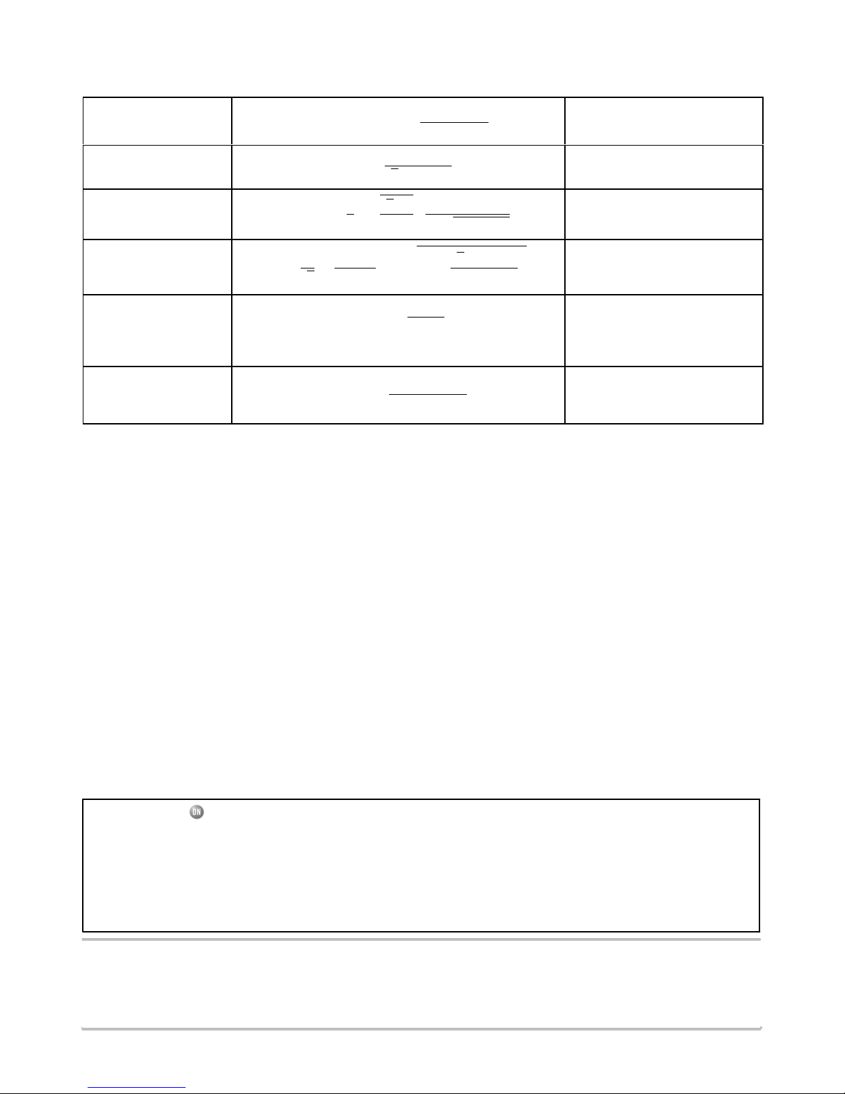
Table 6. SUMMARY OF BOOST EQUATIONS Components are identified in Figure 3 (Continued)
Output Voltage UVP
Detection
Inductor rms Current
Output Diode rms
Current
MOSFET rms Current
V
I
M(RMS)
out(UVP)
I
D(RMS)
+
Ǹ
2
+ V
3
ǒ
@
UVP
I
L(RMS)
4
+
3
P
out
h @ Vac
@ǒR
Ǹ
@
+
@
out1
2 @ P
3Ǹ@ Vac @ h
Ǹ
@ 2
2
p
Ǔ
@ 1 *
Ǹ
R
) R
out2
R
@ R
out2
out
P
@
out
Ǹ
h @ Vac @ V
2Ǹ@ 8 @ Vac
ǒ
3 @ p @ V
FB
FB
) 1
out
out
Ǔ
Ǔ
V
UVP
table.
is shown in the specification
Current Sense Resistor
Type 1 Compensation
P
R
C
R
sense
COMP
sense
+ I
+
V
+
I
L(peak)
M(RMS)
2 @ p @ f
ILIM
2
gm
@ R
sense
CROSS
V
is shown in the specification
ILIM
table.
Where f
quency and is typically less than
20 Hz. gm is shown in the specification table.
is the crossover fre-
CROSS
ON Semiconductor and are registered trademarks of Semiconductor Components Industries, LLC (SCILLC). SCILLC owns the rights to a number of patents, trademarks,
copyrights, trade secrets, and other intellectual property. A listing of SCILLC’s product/patent coverage may be accessed at www.onsemi.com/site/pdf/Patent−Marking.pdf. SCILLC
reserves the right to make changes without further notice to any products herein. SCILLC makes no warranty, representation or guarantee regarding the suitability of its products for any
particular purpose, nor does SCILLC assume any liability arising out of the application or use of any product or circuit, and specifically disclaims any and all liability, including without
limitation special, consequential or incidental damages. “Typical” parameters which may be provided in SCILLC data sheets and/or specifications can and do vary in different applications
and actual performance may vary over time. All operating parameters, including “Typicals” must be validated for each customer application by customer’s technical experts. SCILLC
does not convey any license under its patent rights nor the rights of others. SCILLC products are not designed, intended, or authorized for use as components in systems intended for
surgical implant into the body, or other applications intended to support or sustain life, or for any other application in which the failure of the SCILLC product could create a situation where
personal injury or death may occur. Should Buyer purchase or use SCILLC products for any such unintended or unauthorized application, Buyer shall indemnify and hold SCILLC and
its officers, employees, subsidiaries, affiliates, and distributors harmless against all claims, costs, damages, and expenses, and reasonable attorney fees arising out of, directly or indirectly,
any claim of personal injury or death associated with such unintended or unauthorized use, even if such claim alleges that SCILLC was negligent regarding the design or manufacture
of the part. SCILLC is an Equal Opportunity/Affirmative Action Employer. This literature is subject to all applicable copyright laws and is not for resale in any manner.
PUBLICATION ORDERING INFORMATION
LITERATURE FULFILLMENT:
Literature Distribution Center for ON Semiconductor
P.O. Box 5163, Denver, Colorado 80217 USA
Phone: 303−675−2175 or 800−344−3860 Toll Free USA/Canada
Fax: 303−675−2176 or 800−344−3867 Toll Free USA/Canada
Email: [email protected]
N. American Technical Support: 800−282−9855 Toll Free
USA/Canada
Europe, Middle East and Africa Technical Support:
Phone: 421 33 790 2910
Japan Customer Focus Center
Phone: 81−3−5817−1050
http://onsemi.com
25
ON Semiconductor Website: www.onsemi.com
Order Literature: http://www.onsemi.com/orderlit
For additional information, please contact your local
Sales Representative
EVBUM2162/D
 Loading...