

Page 1
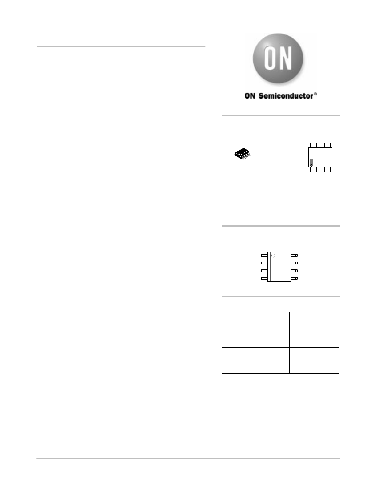
NCP1575
Low Voltage Synchronous
Buck Controller with
Adjustable Switching
Frequency
The NCP1575 is a low voltage buck controller. It provides the
control for a DC−DC power solution producing an output voltage as
low as 0.980 V over a wide current range. It contains all required
circuitry for a synchronous NFET buck regulator using the V
control method to achieve the fastest possible transient response and
best overall regulation. The NCP1575 operates at a default switching
frequency of 200 kHz, but switching frequency is user−programmable
with an additional resistor between R
and ground. This device
OSC
provides undervoltage lockout protection, soft−start, and built−in
adaptive nonoverlap and is assembled in an SOIC−8 package.
The NCP1575−based solution requires a bias supply of 12 V, and it
can convert from a bulk power supply ranging from 2 V to 12 V.
Conversion from bulk supplies greater than 7 V is best accomplished
by using an external doubler circuit to raise the enhancement voltage
for the external NFET switches.
2
http://onsemi.com
MARKING
DIAGRAM
8
8
1
SOIC−8
D SUFFIX
CASE 751
A = Assembly Location
L = Wafer Lot
Y = Year
W = Work Week
1575
ALYW
1
Features
• Pb−Free Packages are Available
• 0.980 V ±1.0% Reference Voltage
2
• V
Control Topology
• 200 ns Transient Response
• Programmable Soft−Start
• 40 ns Gate Rise and Fall Times (3.3 nF Load)
• Adaptive FET Nonoverlap Time
• Default 200 kHz Oscillator Frequency (No External
Resistor Required)
• User−Programmable Oscillator Frequency (One External
Resistor Required)
• Undervoltage Lockout
• On/Off Control Through Use of the COMP Pin
• Overvoltage Protection through Synchronous MOSFETs
• Synchronous N−Channel Buck Design
• “12 V Only” or Dual Supply Operation
PIN CONNECTIONS
18
CC
R
OSC
ORDERING INFORMATION
Device Package Shipping
NCP1575D
NCP1575DG
NCP1575DR2 2500 Tape & Reel
NCP1575DR2G 2500 Tape & Reel
†For information on tape and reel specifications,
including part orientation and tape sizes, please
refer to our Tape and Reel Packaging Specifications
Brochure, BRD8011/D.
SOIC−8
SOIC−8
(Pb−Free)
SOIC−8
SOIC−8
(Pb−Free)
GNDV
V
FB
GATE(L)NC
GATE(H)COMP
98 Units/Rail
98 Units/Rail
†
Semiconductor Components Industries, LLC, 2004
November, 2004 − Rev. 6
1 Publication Order Number
NCP1575/D
Page 2
12 V
NCP1575
BAS20HT1
R1
470
Q3
MMBT3904LT1
D1
18 V Zener
BZX84C18V
D3
C4
1.0 F
Option
BAV99LT1
R3
D2
C11
0.1 F
U1
V
R
NC
COMP
C11
0.1 F
1.0 H
CC
OSC
L1
GATE(L)
GATE(H)
NCP1575
+
C1
1000 F/16 V
GND
V
FB
C3
0.1 F
C9
0.01 F
R5
3.32 k
+
C2
1000 F/16 V
0.98 V
Q1
NTD60N02R
Q2
NTD110N02R
L2
4.7 H
1000 F
R6
5.11 k
C10
4700 pF
+
C5
1000 FC8104
2.5 V/
10 A
+
C6
0.1 F
12 V
33 k
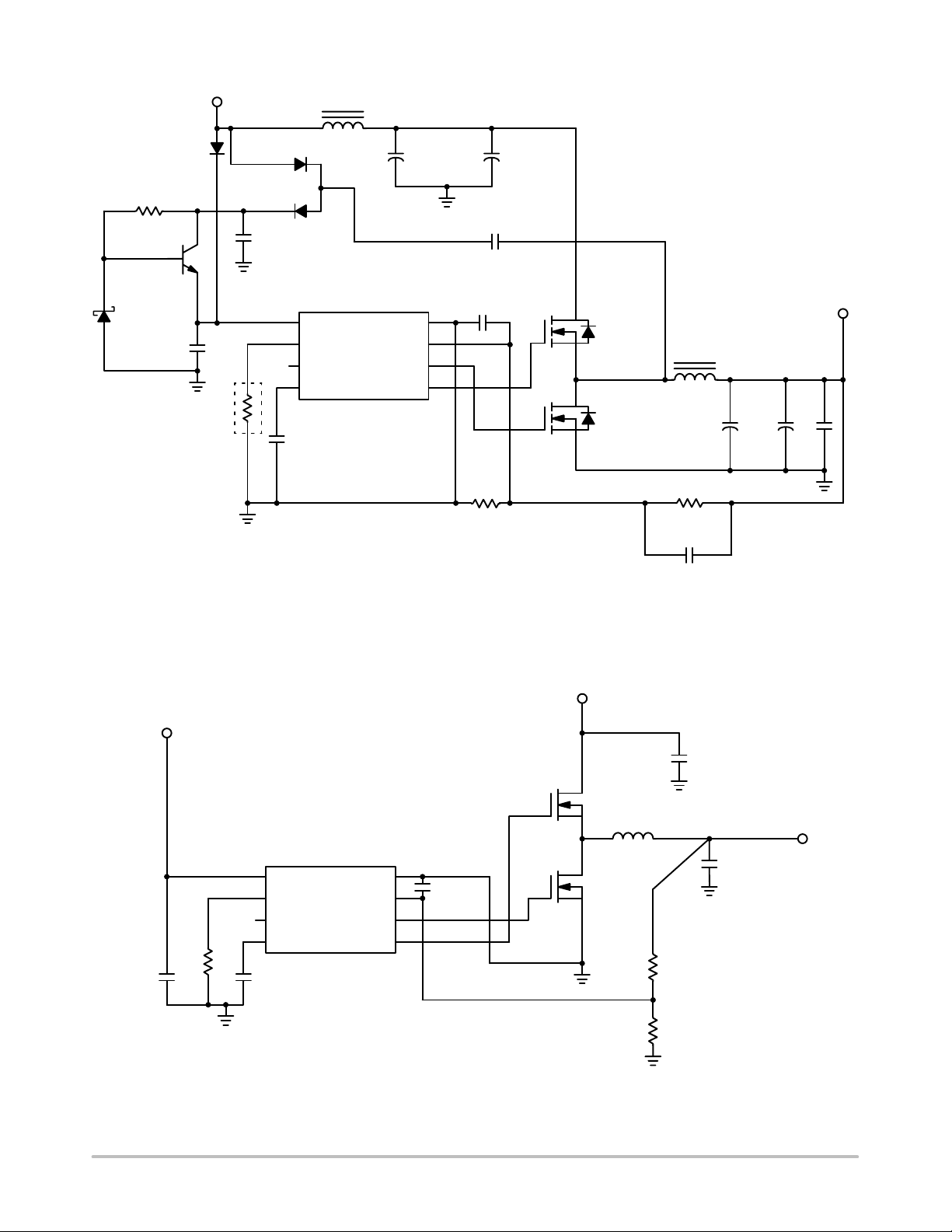
Figure 1. 12 V Only Applications Diagram, 12 V to 2.5 V Conversion at 10 A
5 V
33 F
8 V/1.6 A RMS × 2
Specialty Polymer
60 m ESR
2.26 k
10 k
V
R
NC
COMP
0.1 F
CC
OSC
NCP1575
GATE(L)
GATE(H)
GND
V
FB
1000 pF
NTD4302
1.4 H
NTD4302
1.2 V/ 10 A
56 F
4 V/1.6 A RMS × 2
Specialty Polymer
40 m ESR
Figure 2. 12 V/5 V Applications Diagram, 350 kHz, 5 V to 1.2 V Conversion at 10 A
http://onsemi.com
2
Page 3
12 V
NCP1575
D1
5.6 V Zener
BZX84C5V6
R1
15
C4
205
Option
open
R3
R7
15
D2
BAV99LT1
L1
1.0 H
U1
V
R
NC
COMP
C11
0.1 F
CC
OSC
GATE(L)
GATE(H)
NCP1575
+
C1
1000 F/16 V
GND
V
FB
R5
3.3 k
+
C2
1000 F/16 V
C3*
0.033 F
C9
10000 pF
0.98 V
5.1 k
4700 pF
R6
C10
Q1
NTD30N02
L2
2.4 H
Q4
NTD30N02
1000 F
+
C5
1000 FC8104
C6
*C3 value is dependent on MOSFET
gate drive current. Incorrect values
may cause poor V
excessive power dissipation in D1.
regulation or
CC
2.5 V/
6.0 A
+
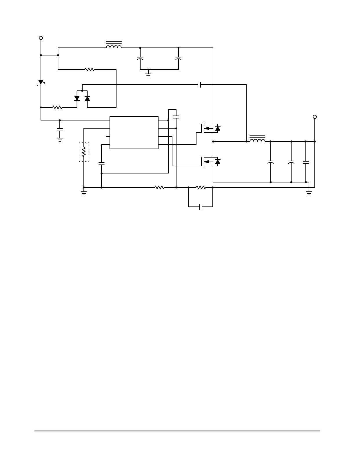
Figure 3. 12 V Only Applications Diagram, 12 V to 2.5 V Conversion at 6 A
http://onsemi.com
3
Page 4
NCP1575
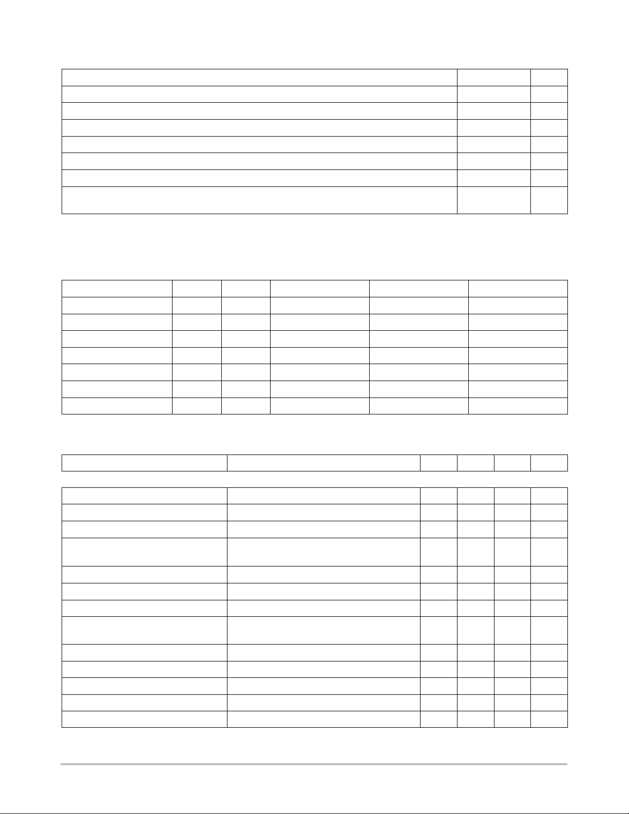
MAXIMUM RATINGS
Rating Value Unit
Operating Junction Temperature 150 °C
Storage Temperature Range −65 to 150 °C
ESD Susceptibility (Human Body Model) 2.0 kV
ESD Susceptibility (Charged Device Model) 200 V
Lead Temperature Soldering: Reflow: (Note 1) 230 peak °C
Moisture Sensitivity Level 2 −
Package Thermal Resistance, SOIC−8: Junction−to−Case, R
Junction−to−Ambient, R
JC
JA
Maximum ratings are those values beyond which device damage can occur. Maximum ratings applied to the device are individual stress limit
values (not normal operating conditions) and are not valid simultaneously . If these limits are exceeded, device functional operation is not implied,
damage may occur and reliability may be affected.
1. 60 second maximum above 183°C.
MAXIMUM RATINGS
Pin Name Symbol V
IC Power Input V
CC
MAX
20 V −0.5 V N/A 1.5 A Peak, 450 mA DC
Compensation Capacitor COMP 6.0 V −0.5 V 10 mA 10 mA
Voltage Feedback Input V
Frequency Adjust R
FB
OSC
6.0 V −0.5 V 1.0 mA 1.0 mA
6.0 V −0.5 V 1.0 mA 1.0 mA
High−Side FET Driver GATE(H) 20 V −0.5 V, −2.0 V for 50 ns 1.5 A Peak, 200 mA DC 1.5 A Peak, 200 mA DC
Low−Side FET Driver GATE(L) 20 V −0.5 V , −2.0 V for 50 ns 1.5 A Peak, 200 mA DC 1.5 A Peak, 200 mA DC
Ground GND 0.5 V −0.5 V 1.5 A Peak, 450 mA DC N/A
V
MIN
I
SOURCE
48
165
I
SINK
°C/W
°C/W
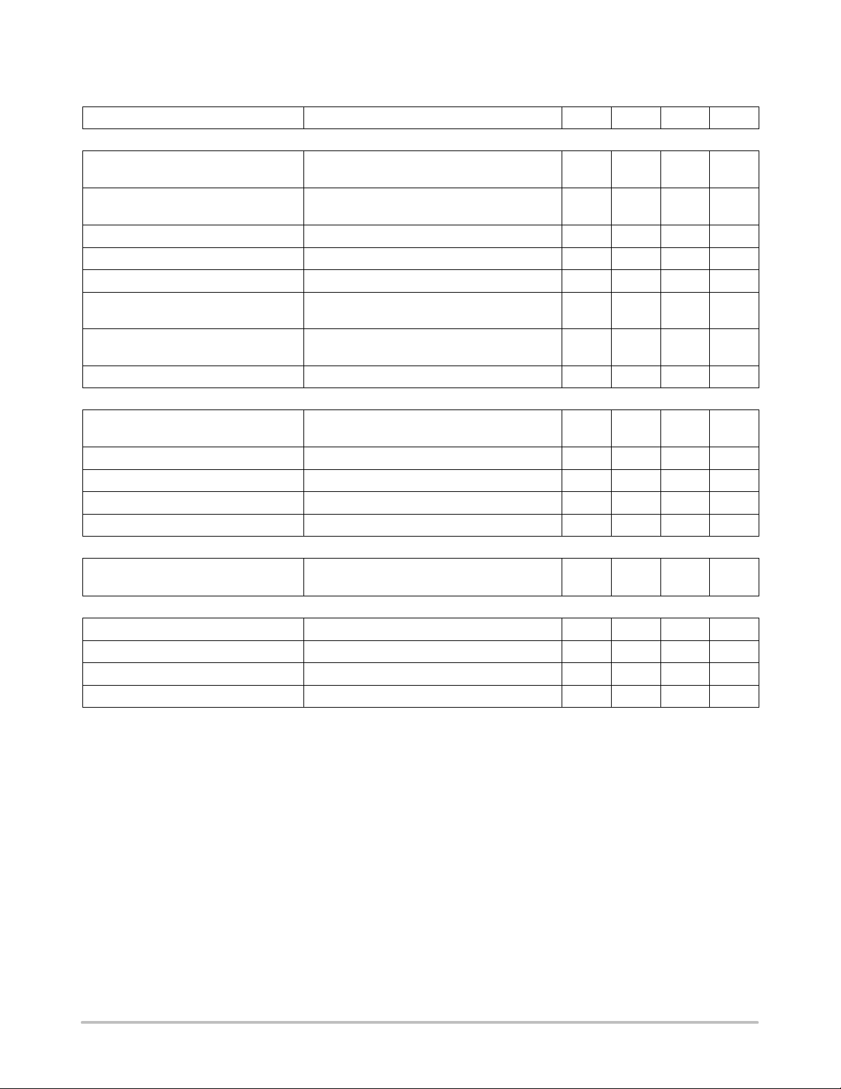
ELECTRICAL CHARACTERISTICS (0°C < T
C
COMP
= 0.1 F, R
= 74 k; unless otherwise specified.) Note 2
OSC
Characteristic
< 125°C, 9.0 V < VCC < 20 V, C
J
Test Conditions Min Typ Max Unit
GATE(H)
= C
GATE(L)
= 3.3 nF,
Error Amplifier
Bias Current VFB = 0 V − 0.4 2.0 A
V
FB
COMP Source Current COMP = 1.5 V, VFB = 0.8 V 15 30 60 A
COMP Sink Current COMP = 1.5 V, VFB = 1.2 V 15 30 60 A
Reference Voltage COMP = V
TJ < 25°C
FB
0.970
0.965
0.980
0.980
0.990
0.995
COMP Max Voltage VFB = 0.8 V 2.4 3.1 − V
COMP Min Voltage VFB = 1.2 V − 0.1 0.2 V
COMP Fault Discharge Current at UVLO COMP = 1.2 V, VCC = 6.9 V 0.5 1.2 − mA
COMP Fault Discharge Threshold to
− 0.1 0.25 0.3 V
Reset UVLO
Open Loop Gain − − 98 − dB
Unity Gain Bandwidth − − 20 − kHz
PSRR @ 1.0 kHz − − 70 − dB
Output Transconductance − − 32 − mmho
Output Impedance − − 2.5 − M
2. Characteristics at temperature extremes are guaranteed via correlation using quality statistical control methods.
V
V
http://onsemi.com
4
Page 5
NCP1575
ELECTRICAL CHARACTERISTICS (0°C < T
C
COMP
= 0.1 F, R
= 74 k; unless otherwise specified.) Note 3
OSC
Characteristic
< 125°C, 9.0 V < VCC < 20 V, C
J
Test Conditions Min Typ Max Unit
GATE(H)
= C
GATE(L)
= 3.3 nF,
GATE(H) and GATE(L)
Rise Time 1.0 V < GATE(L), GATE(H) < VCC − 2.0 V,
V
= 12 V
CC
Fall Time VCC − 2.0 V < GATE(L), GATE(H) < 1.0 V,
V
= 12 V
CC
− 40 80 ns
− 40 80 ns
GATE(H) to GATE(L) Delay GATE(H) < 2.0 V, GATE(L) > 2.0 V 40 60 105 ns
GATE(L) to GATE(H) Delay GATE(L) < 2.0 V, GATE(H) > 2.0 V 40 60 105 ns
Minimum Pulse Width GATE(X) = 4.0 V − 250 − ns
High Voltage (AC) Measure GATE(L) or GATE(H)
0.5 nF < C
GATE(H)
= C
GATE(L)
Low Voltage (AC) Measure GATE(L) or GATE(H)
0.5 nF < C
GATE(H)
= C
GATE(L)
< 10 nF, Note 4
< 10 nF, Note 4
VCC −
0.5
V
CC
− V
− 0 0.5 V
GATE(H)/(L) Pull−Down Resistance to GND. Note 4 20 50 115 k
PWM Comparator
PWM Comparator Offset VFB = 0 V, Increase COMP Until GATE(H)
0.415 0.465 0.525 V
Starts Switching
Ramp Max Duty Cycle − − 80 − %
Artificial Ramp Duty Cycle = 50%, R
= 74 k 50 63 75 mV
OSC
Transient Response COMP = 1.5 V, VFB 20 mV Overdrive. Note 4 − 200 300 ns
VFB Input Range Note 4 0 − 1.4 V
Oscillator
Switching Frequency R
R
OSC
OSC
Not Used
= 74 k
170
240
200
280
230
320
General Electrical Specifications
V
Supply Current COMP = 0 V (No Switching) − 9.0 12 mA
CC
Start Threshold GATE(H) Switching, COMP Charging 8.0 8.5 9.0 V
Stop Threshold GATE(H) Not Switching, COMP Discharging 7.0 7.5 8.0 V
Hysteresis Start − Stop 0.75 1.0 1.25 V
3. Characteristics at temperature extremes are guaranteed via correlation using quality statistical control methods.
4. Guaranteed by design. Not tested in production.
kHz
kHz
http://onsemi.com
5
Page 6
NCP1575
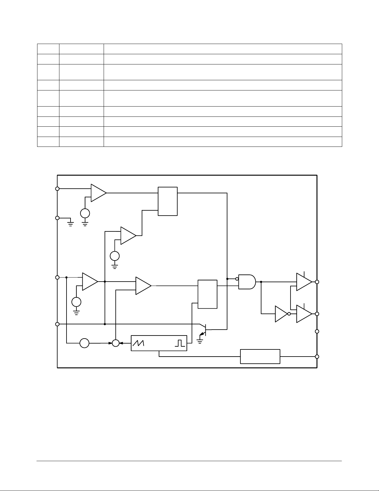
PACKAGE PIN DESCRIPTION
PIN # PIN SYMBOL FUNCTION
1 V
2 R
CC
OSC
3 NC No connect.
4 COMP Error amp output. PWM comparator reference input. A capacitor to LGND provides error amp compensa-
5 GATE(H) High−side switch FET driver pin. Capable of delivering peak currents of 1.5 A.
6 GATE(L) Low−side synchronous FET driver pin. Capable of delivering peak currents of 1.5 A.
7 V
FB
8 GND Power supply return.
Power supply input.
Frequency adjust pin. If not used, oscillator frequency is nominally 200 kHz. Connecting R
through a single resistor will increase oscillator frequency.
OSC
tion and Soft−Start. Pulling pin < 0.415 V locks gate outputs to a zero percent duty cycle state.
Error amplifier and PWM comparator input.
to ground
V
CC
GND
V
FB
COMP
+
−
Error Amp
−
+
+
−
0.98 V
− +
0.465 V
UVLO Comp
−
+
8.5 V/7.5 V
+
−
−
+
0.25 V
UVLO Latch
PWM Comp
−
+
Oscillator
200 kHz
SQ
R
Set
Dominant
PWM Latch
RQ
S
Reset
Dominant
Nonoverlap
Frequency
Adjust
V
CC
GATE(H)
V
CC
GATE(L)
NC
R
OSC
Figure 4. Block Diagram
http://onsemi.com
6
Page 7
10
NCP1575
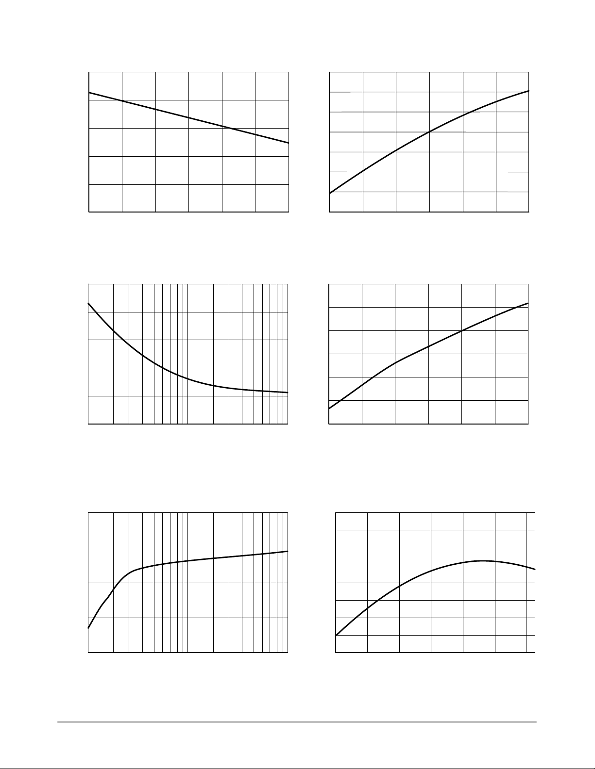
TYPICAL PERFORMANCE CHARACTERISTICS
216
9
8
(mA)
CC
I
7
6
5
0
20 40 60 80 100 120
Temperature (°C)
214
212
210
208
206
Oscillator Frequency (kHz)
204
202
0
20 40 60 80 120100
Temperature (°C)
Figure 5. Supply Current vs. Temperature Figure 6. Oscillator Frequency vs. Temperature
600
500
400
300
(No R
300
295
290
285
280
OSC
)
200
Oscillator Frequency (kHz)
100
10
100 1000 0
Value (k)
R
OSC
Figure 7. Oscillator Frequency vs. R
70
65
60
Artificial Ramp (mV)
55
50
10
100 1000
R
Value (k)
OSC
Oscillator Frequency (kHz)
275
270
Value Figure 8. Oscillator Frequency (R
OSC
20 40 60 80 120
Temperature (°C)
vs. Temperature
0.984
0.983
0.982
0.981
0.980
0.979
0.978
Reference Voltage (V)
0.977
0.976
0
20 40 60 80 100 120
Temperature (°C)
OSC
100
= 74 k)
Figure 9. Artificial Ramp at 50% Duty Cycle
vs. R
OSC
Value
Figure 10. Reference Voltage vs. Temperature
http://onsemi.com
7
Page 8
470
NCP1575
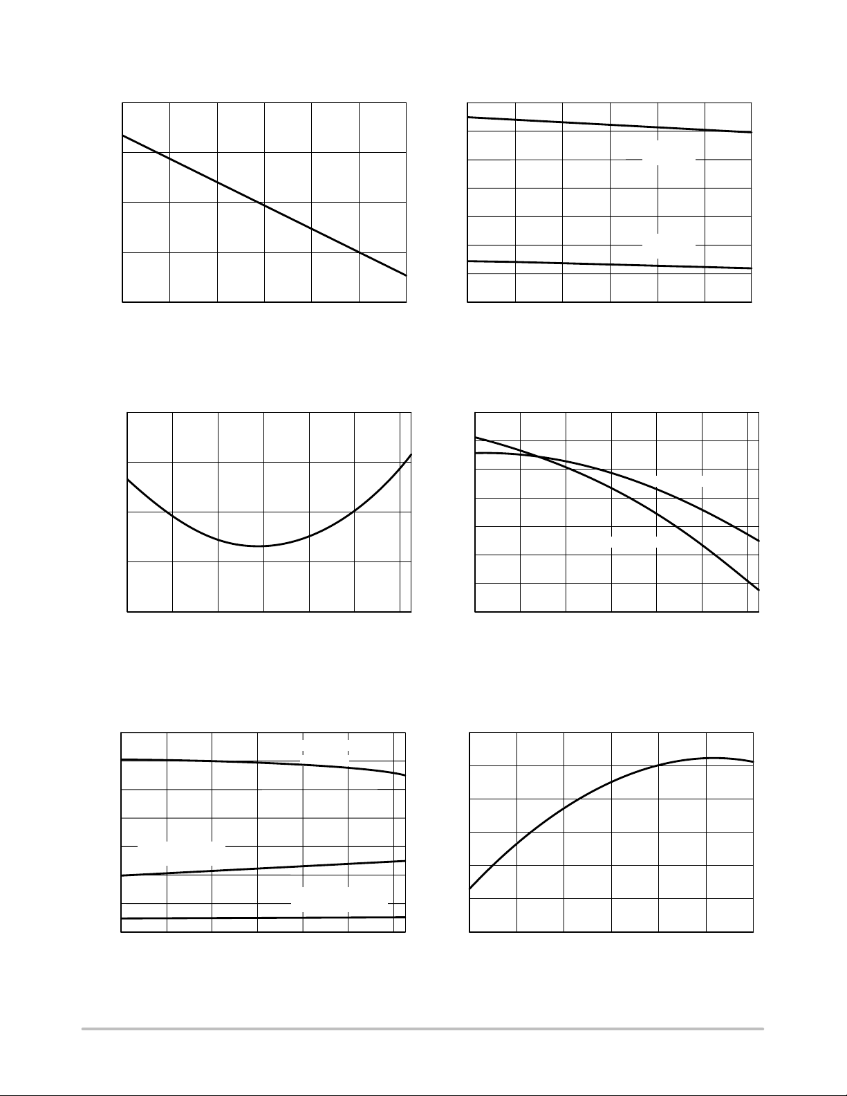
TYPICAL PERFORMANCE CHARACTERISTICS
8.6
465
460
455
PWM Offset Voltage (mV)
450
0
20 40 60 80 100 120
Temperature (°C)
8.4
8.2
8.0
7.8
7.6
7.4
Start/Stop Threshold Voltages (V)
7.2
0
20 40 60 80 120100
Temperature (°C)
Turn−On
Threshold
Turn−Off
Threshold
Figure 11. PWM Offset Voltage vs. Temperature Figure 12. Undervoltage Lockout Thresholds vs.
Temperature
0.60
0.55
0.50
Bias Current (A)
0.45
31
30
29
28
27
Source Current
26
Output Current (A)
25
Sink Current
0.40
0
Figure 13. V
3.5
3.0
2.5
2.0
1.5
1.0
COMP Voltages (V)
0.5
0
0
20 40 60 80 100 120
Temperature (°C)
Bias Current vs. Temperature Figure 14. Error Amp Output Currents vs. Temperature
FB
COMP Maximum
COMP Minimum
Voltage
Threshold Voltage
20 40 60 80 100 120
Temperature (°C)
Figure 15. COMP Voltages vs. Temperature
Voltage
COMP Fault
24
0
20 40 60 80 100 120
Temperature (°C)
1.20
1.15
1.10
1.05
1.00
Discharge Current (mA)
0.95
0.90
0
20 40 60 80 100 120
Temperature (°C)
Figure 16. COMP Fault Mode Discharge Current vs.
Temperature
http://onsemi.com
8
Page 9
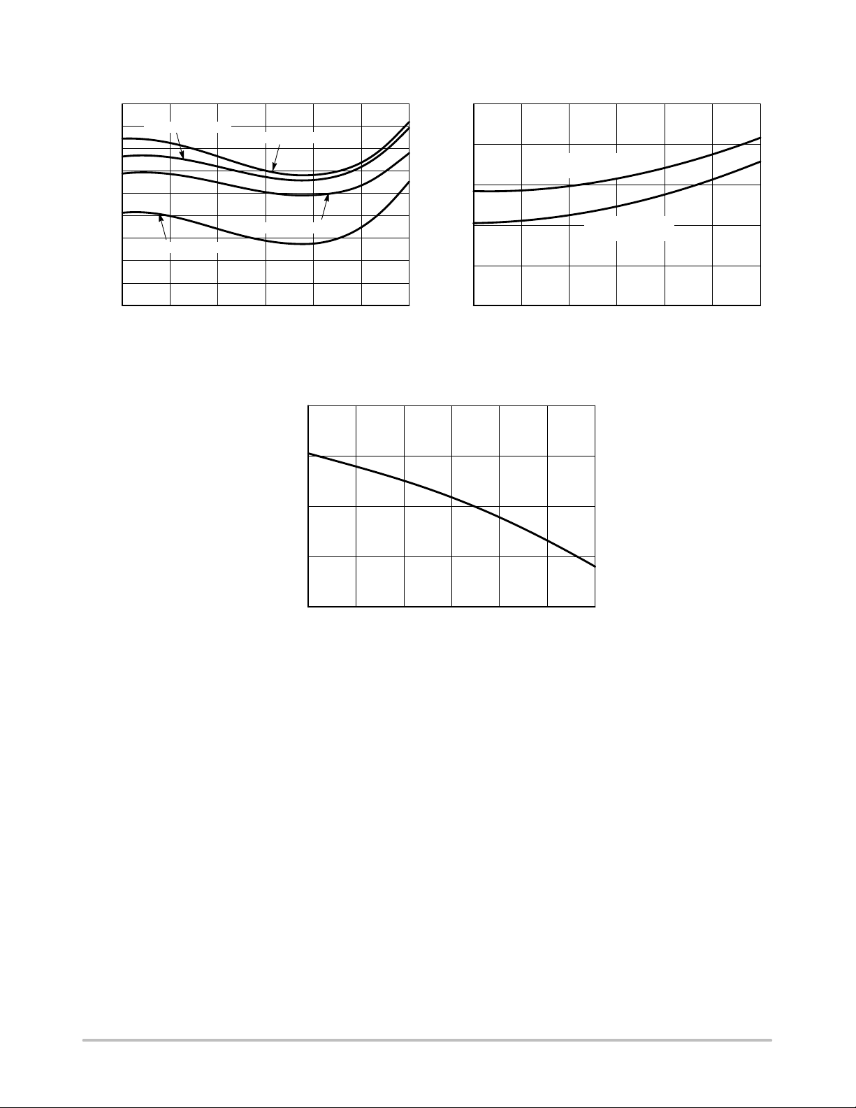
38
36
34
32
30
28
26
24
GATE Rise/Fall Times (ns)
22
20
0
TYPICAL PERFORMANCE CHARACTERISTICS
GATEH Fall Time
GATEL Fall Time
20 40 60 80 120100
GATEH Rise Time
GATEL Rise Time
Temperature (°C)
NCP1575
55
50
45
40
35
Gate Non−Overlap Time (ns)
30
GATEH to GATEL
Delay Time
GATEL to GATEH
Delay Time
0
20 40 60 80 100 120
Temperature (°C)
Figure 17. GATE Output Rise and Fall Times vs.
Temperature (VCC = 12 V)
70
65
60
Artificial Ramp (mV)
55
50
0
20 40 60 80 120
Figure 19. Artificial Ramp at 50% Duty Cycle
Figure 18. GATE Nonoverlap Times vs. Temperature
Temperature (°C)
(R
Not Used)
OSC
100
http://onsemi.com
9
Page 10
NCP1575
APPLICATION INFORMATION
THEORY OF OPERATION
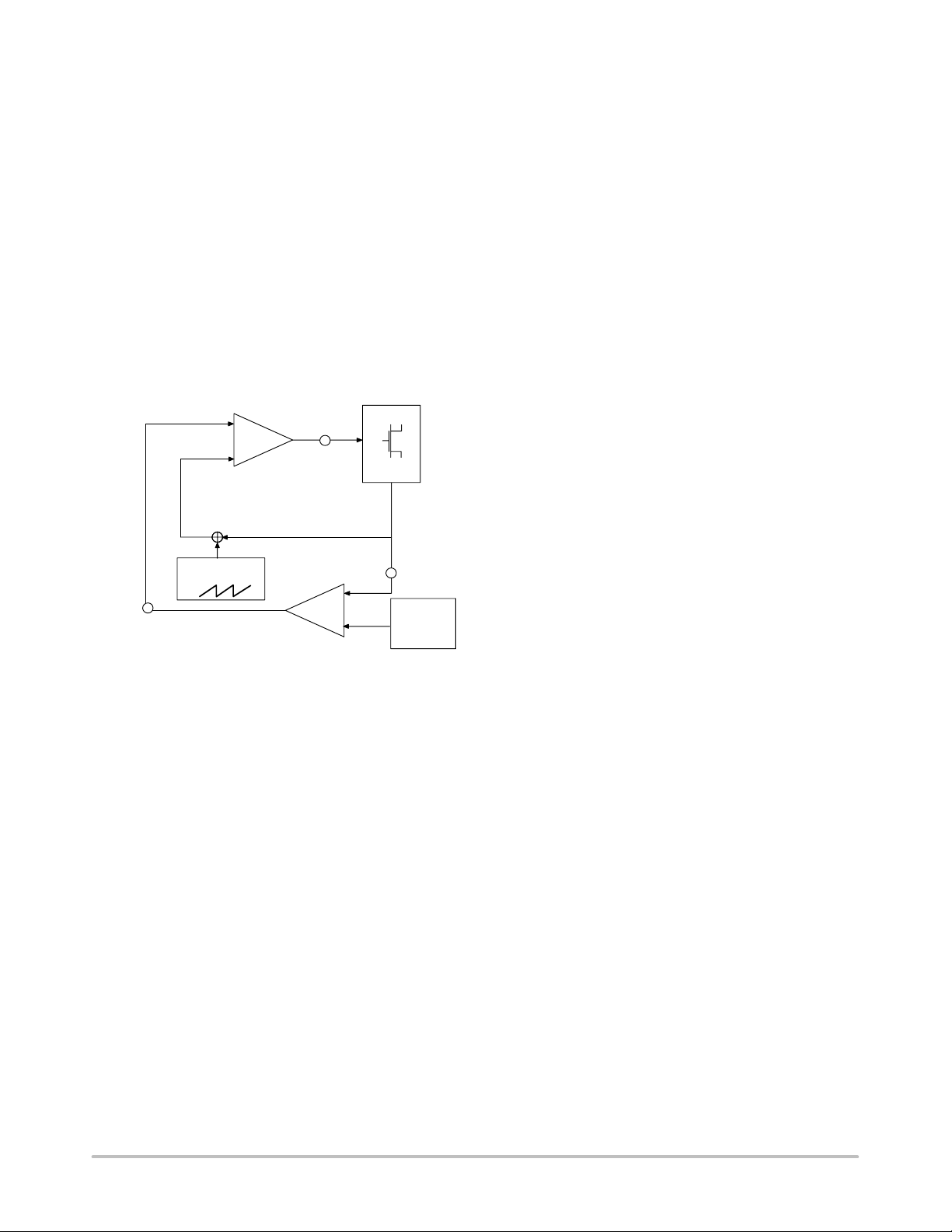
The NCP1575 is a simple, synchronous, fixed−frequency,
low−voltage buck controller using the V2 control method.
V2 Control Method
The V2 control method uses a ramp signal generated by
the ESR of the output capacitors. This ramp is proportional
to the ac current through the main inductor and is offset by
the dc output voltage. This control scheme inherently
compensates for variation in either line or load conditions,
since the ramp signal is generated from the output voltage
itself. The V
2
method differs from traditional techniques
such as voltage mode control, which generates an artificial
ramp, and current mode control, which generates a ramp
using the inductor current.
−
PWM
+
RAMP
Slope
Compensation
COMP
Figure 20. V2 Control with Slope Compensation
Error
Signal
GATE(H)
GATE(L)
Error
Amplifier
Output
Voltage
V
FB
−
+
Reference
Voltage
The error signal loop can have a low crossover frequency,
since the transient response is handled by the ramp signal
loop. The main purpose of this ‘slow’ feedback loop is to
provide dc accuracy. Noise immunity is significantly
improved, since the error amplifier bandwidth can be rolled
off at a low frequency. Enhanced noise immunity improves
remote sensing of the output voltage, since the noise
associated with long feedback traces can be effectively
filtered.
Line and load regulation are drastically improved because
there are two independent control loops. A voltage mode
controller relies on the change in the error signal to
compensate for a deviation in either line or load voltage.
This change in the error signal causes the output voltage to
change corresponding to the gain of the error amplifier,
which is normally specified as line and load regulation. A
current mode controller maintains a fixed error signal during
line transients, since the slope of the ramp signal changes in
this case. However , r egulation o f l oad t ransients still requires
a change in the error signal. The V
2
method of control
maintains a f ixed e rror s ignal f or b oth l ine a nd l oad v ariation,
since the ramp signal is affected by both line and load.
The stringent load transient requirements of modern
microprocessors require the output capacitors to have very
low ESR. T he r esulting s hallow s lope i n t he o utput r ipple can
lead to p ulse w idth j itter a nd variation caused b y b oth r andom
and synchronous noise. A ramp waveform generated in the
oscillator is added to the r amp s ignal f rom the o utput v oltage
to provide the proper voltage ramp at the beginning of each
switching cycle. This s lope c ompensation i ncreases t he n oise
immunity, particularly at duty cycles above 50%.
The V2 control method is illustrated in Figure 20. The
output voltage generates both the error signal and the ramp
signal. Since the ramp signal is simply the output voltage, it
is affected by any change in the output, regardless of the
origin of that change. The ramp signal also contains the DC
portion of the output voltage, allowing the control circuit to
drive the main switch from 0% to 100% duty cycle as
required.
A variation in line voltage changes the current ramp in the
inductor, which causes the V
2
control scheme to compensate
the duty cycle. Since any variation in inductor current
modifies the ramp signal, as in current mode control, the V
control scheme offers the same advantages in line transient
response.
A variation in load current will affect the output voltage,
modifying the ramp signal. A load step immediately changes
the state of the comparator output, which controls the main
switch. The comparator response time and the transition
speed of the main switch determine the load transient
response. Unlike traditional control methods, the reaction
time to the output load step is not related to the crossover
frequency of the error signal loop.
Startup
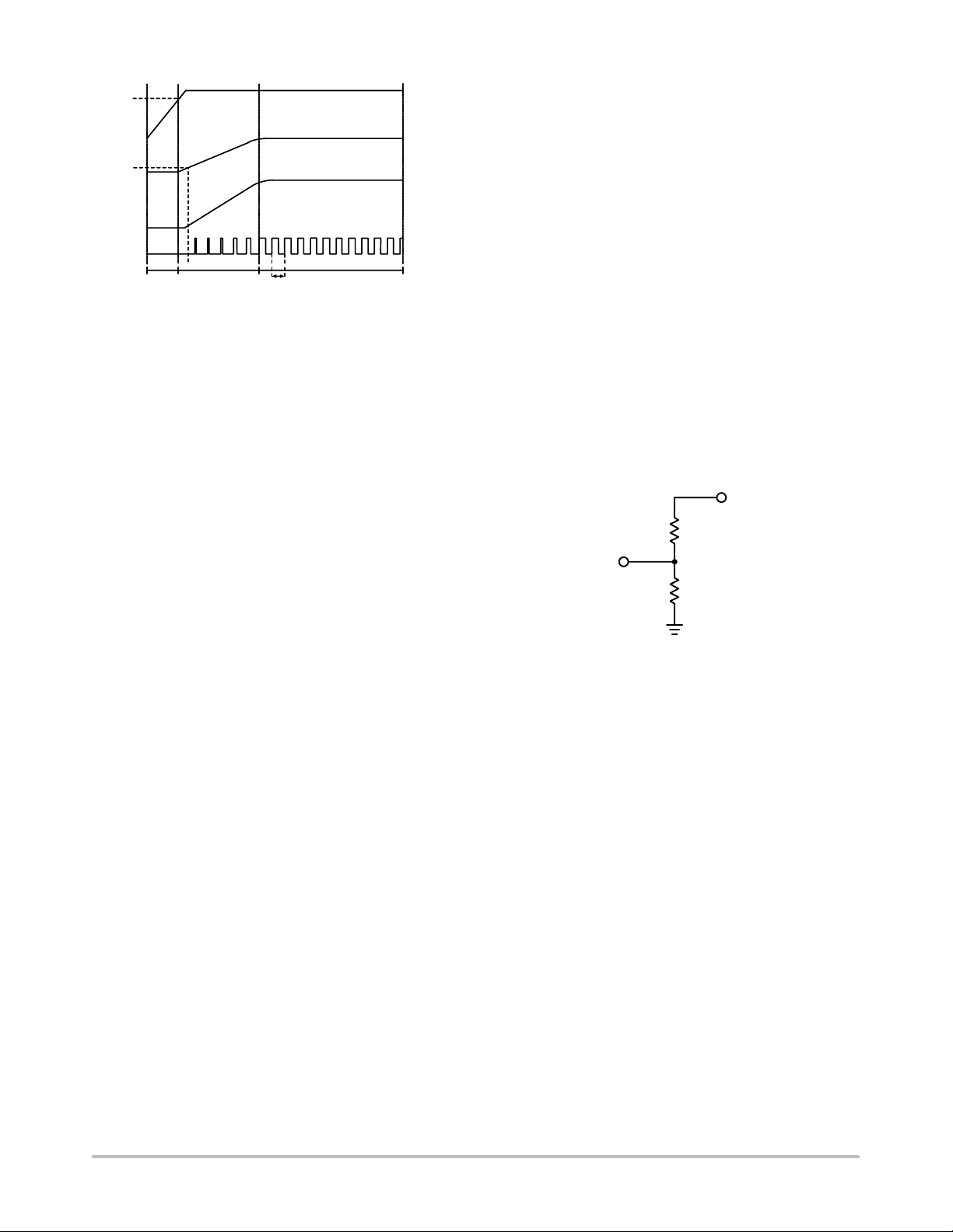
The NCP1575 features a programmable soft−start
function, which is implemented through the error amplifier
and the external compensation capacitor. This feature
prevents stress to the power components and limits output
voltage overshoot during startup. As power is applied to the
regulator, the NCP1575 undervoltage lockout circuit (UVL)
monitors the IC’s supply voltage (V
). The UVL circuit
CC
holds the GATE(H) output low and the GATE(L) output
high until VCC exceeds the 8.5 V threshold. A hysteresis
function of 1.0 V improves noise immunity. The
2
compensation capacitor connected to the COMP pin is
charged by a 30 A current source. When the capacitor
voltage exceeds the 0.465 V offset of the PWM comparator,
the PWM control loop will allow switching to occur. The
upper gate driver GATE(H) is activated, turning on the upper
MOSFET. The current ramps up through the main inductor
and linearly powers the output capacitors and load. When
the regulator output voltage exceeds the COMP pin voltage
minus the 0.465 V PWM comparator offset threshold and
the artificial ramp, the PWM comparator terminates the
initial pulse.
http://onsemi.com
10
Page 11
NCP1575
V
8.5 V
0.465 V
UVLO STARTUP NORMAL OPERATION
Figure 21. Idealized Waveforms
Normal Operation
t
S
IN
V
COMP
V
FB
GATE(H)
During normal operation, t he d uty c ycle o f t he g ate d rivers
remains approximately constant as the V2 control loop
maintains the regulated output voltage under steady state
conditions. Variations in supply l ine o r o utput l oad c onditions
will result in changes in duty cycle to maintain regulation.
Input Supplies
The NCP1575 can be used in applications where a 12 V
supply is available along with a lower voltage supply. Often
the lower voltage supply is 5 V, but it can be any voltage less
than the 12 V supply minus the required gate drive voltage
of the top MOSFET. The greater the difference between the
two voltages, the better the efficiency due to increasing V
GS
available to turn on the upper MOSFET. In order to maintain
power supply stability, the lower supply voltage should be
at least 1.5 times the desired voltage.
Adding a few additional components allows the NCP1575
to convert power in a “12 V only” application. This circuit
is illustrated in Figure 1. Note that in all cases, the maximum
supply voltage s pecification of 20 V must not be exceeded.
Gate Charge Effect on Switching Times
When using the onboard gate drivers, the gate charge has
an important effect on the switching times of the FETs. A
finite amount of time is required to charge the effective
capacitor seen at the gate of the FET. Therefore, the rise and
fall times rise linearly with increased capacitive loading.
Transient Response
The 200 ns reaction time of the control loop provides fast
transient response to any variations in input voltage and
output current. Pulse−by−pulse adjustment of duty cycle is
provided to quickly ramp the inductor current to the required
level. Since the inductor current cannot be changed
instantaneously, regulation is maintained by the output
capacitors during the time required to slew the inductor
current. For better transient response, several high
frequency and bulk output capacitors are usually used.
Overvoltage Protection
Overvoltage protection is provided as a result of the
normal operation of the V2 control method and requires no
additional external components. The control loop responds
to an overvoltage condition within 200 ns, turning off the
upper MOSFET and disconnecting the regulator from its
input voltage. This results in a crowbar action to clamp the
output voltage, preventing damage to the load. The regulator
remains in this state until the overvoltage condition ceases.
Shutdown
When the input voltage connected t o VCC falls through the
lower threshold of the UVLO comparator, a fault latch is set.
The fault latch provides a signal that forces both GATE(H)
low and GATE(L) high, producing a low−impedance current
sink to ground at the converter switch node. At the same
time, the latch also turns on a transistor which pulls down on
the COMP pin, quickly discharging the external capacitor,
and allowing COMP to fall.
CONVERTER DESIGN
Choosing the V
Resistor Divider Values
OUT
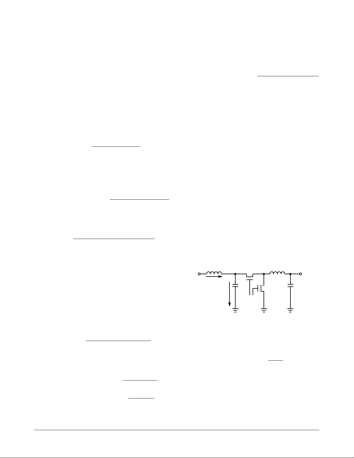
The NCP1575 has an internal 0.98 V reference. A resistor
divider is used to set the output voltage.
V
OUT
R1
V
FB
R2
Figure 22.
The formula to set the output voltage is
V
(R1R2 1) (0.98 V)
OUT
Arbitrarily choose a value of R2 that is sufficiently low
that the VFB bias current (typically 50 nA) will have
negligible effect on the output voltage. Solve the equation
above for the value of R1.
Choosing the Oscillator Frequency
The NCP1575 has an oscillator that is trimmed to 200 kHz
at the factory. The NCP1575 will operate at this frequency
without the addition of any external components. However,
the oscillator is user−programmable with a single resistor.
This resistor is connected between the R
pin and ground.
OSC
Adding this resistor will raise the frequency above 200 kHz.
A graph of oscillator frequency vs. R
resistance is
OSC
provided in the typical operating characteristics section of
this data sheet.
Selection of the Output Capacitors
These components must be selected and placed carefully
to yield optimal results. Capacitors should be chosen to
provide acceptable ripple on the regulator output voltage.
Key specifications for output capacitors are their Equivalent
http://onsemi.com
11
Page 12

NCP1575
Series Resistance (ESR), and Equivalent Series Inductance
(ESL). For best transient response, a combination of low
value/high frequency and bulk capacitors placed close to the
load will be required.
In order to determine the number of output capacitors the
maximum voltage transient allowed during load transitions
has to be specified. The output capacitors must hold the
output voltage within these limits since the inductor current
can not change with the required slew rate. The output
capacitors must therefore have a very low ESL and ESR.
The voltage change during the load current transient is:
V
OUT
I
OUT
ESL
ESR
t
C
t
TR
OUT
where:
I
/ t = load current slew rate;
OUT
I
= load transient;
OUT
t = load transient duration time;
ESL = Maximum allowable ESL including capacitors,
circuit traces, and vias;
ESR = Maximum allowable ESR including capacitors
and circuit traces;
t
= output voltage transient response time.
TR
The designer has to independently assign values for the
change in output voltage due to ESR, ESL, and output
capacitor discharging or charging. Empirical data indicates
that most of the output voltage change (droop or spike
depending on the load current transition) results from the
total output capacitor ESR.
The maximum allowable ESR can then be determined
according to the formula:
V
ESR
MAX
I
ESR
OUT
where:
V
= change in output voltage due to ESR (assigned
ESR
by the designer)
Once the maximum allowable ESR is determined, the
number of output capacitors can be found by using the
formula:
ESR
Number of capacitors
ESR
CAP
MAX
where:
ESR
= maximum ESR per capacitor (specified in
CAP
manufacturer’s data sheet).
ESR
= maximum allowable ESR.
MAX
The actual output voltage deviation due to ESR can then
be verified and compared to the value assigned by the
designer:
V
ESR
I
OUT
ESR
MAX
Similarly, the maximum allowable ESL is calculated from
the following formula:
ESL
MAX
V
ESL
I
t
Selection of the Input Inductor
A common requirement is that the buck controller must
not disturb the input voltage. One method of achieving this
is by using an input inductor and a bypass capacitor. The
input inductor isolates the supply from the noise generated
in the switching portion of the buck regulator and also limits
the inrush current into the input capacitors upon power up.
The inductor’s limiting effect on the input current slew rate
becomes increasingly beneficial during load transients. The
worst case is when the load changes from no load to full load
(load step), a condition under which the highest voltage
change across the input capacitors is also seen by the input
inductor. The inductor successfully blocks the ripple current
while placing the transient current requirements on the input
bypass capacitor bank, which has to initially support the
sudden load change.
The minimum inductance value for the input inductor is
therefore:
V
(dIdt)
MAX
L
IN
where:
LIN = input inductor value;
V = voltage seen by the input inductor during a full load
swing;
(dI/dt)
= maximum allowable input current slew rate.
MAX
The designer must select the LC filter pole frequency so
that at least 40 dB attenuation is obtained at the regulator
switching frequency . The LC filter is a double−pole network
with a slope of −2.0, a roll−off rate of −40 dB/dec, and a
corner frequency:
2 LC
1
f
C
where:
L = input inductor;
C = input capacitor(s).
Selection of the Output Inductor
There are many factors to consider when choosing the
output inductor. Maximum load current, core and winding
losses, ripple current, short circuit current, saturation
characteristics, component height and cost are all variables
that the designer should consider. However, the most
important consideration may be the effect inductor value has
on transient response.
The amount of overshoot or undershoot exhibited during
a current transient is defined as the product of the current
step and the output filter capacitor ESR. Choosing the
inductor value appropriately can minimize the amount of
energy that must be transferred from the inductor to the
capacitor or vice−versa. In the subsequent paragraphs, we
will determine the minimum value of inductance required
for our system and consider the trade−off of ripple current
vs. transient response.
http://onsemi.com
12
Page 13
NCP1575
In order to choose the minimum value of inductance, input
voltage, output voltage and output current must be known.
Most computer applications use reasonably well regulated
bulk power supplies so that, while the equations below
specify V
IN(MAX)
nominal value of V
or V
in these calculations with little error.
IN
, it is possible to use the
IN(MIN)
Current in the inductor while operating in the continuous
current mode is defined as the load current plus ripple
current.
IL I
LOAD
I
RIPPLE
The ripple current waveform is triangular, and the current
is a function of voltage across the inductor, switch FET
on−time and the inductor value. FET on−time can be defined
as the product of duty cycle and switch frequency, and duty
cycle can be defined as a ratio of V
(
I
RIPPLE
VIN V
(
f
OSC
to VIN. Thus,
OUT
)
V
OUT
)(L)(
V
IN
OUT
)
Peak inductor current is defined as the load current plus
half of the peak current. Peak current must be less than the
maximum rated FET switch current, and must also be less
than the inductor saturation current. Thus, the maximum
output current can be defined as:
I
OUT(MAX)
I
SWITCH(MAX)
V
IN(MAX)
2
f
OSC
V
L
OUT
V
IN(MAX)
V
OUT
Since the maximum output current must be less than the
maximum switch current, the minimum inductance required
can be determined.
L
(MIN)
(
f
(
OSC
V
IN(MIN)
)(
I
V
SWITCH(MAX)
OUT
)
V
OUT
)(
V
IN(MIN)
)
This equation identifies the value of inductor that will
provide the full rated switch current as inductor ripple
current, and will usually result in inefficient system
operation. The system will sink current away from the load
during some portion of the duty cycle unless load current is
greater than half of the rated switch current. Some value
larger than the minimum inductance must be used to ensure
the converter does not sink current. Choosing larger values
of inductor will reduce the ripple current, and inductor value
can be designed to accommodate a particular value of ripple
current by replacing I
I
:
RIPPLE
L
(RIPPLE)
SWITCH(MAX)
(
V
IN(MIN)
(
f
OSC
with a desired value of
OUT
)(
V
)
V
IN(MIN)
)(
I
RIPPLE
V
OUT
)
However, reducing the ripple current will cause transient
response times to increase. The response times for both
increasing and decreasing current steps are shown below.
T
RESPONSE(INCREASING)
T
RESPONSE(DECREASING)
(L)(
(
VIN V
(L)(
(
I
I
V
OUT
OUT
OUT
OUT
)
)
)
)
Inductor value selection a lso d epends o n h ow m uch o utput
ripple voltage the system can tolerate. Output ripple voltage
is defined as the product of the output ripple current and the
output filter capacitor ESR.
Thus, output ripple voltage can be calculated as:
V
RIPPLE
ESR
C
I
RIPPLE
ESR
VIN V
C
f
OSC
L
OUT
V
IN
V
OUT
Finally, we should consider power dissipation in the
output inductors. Power dissipation is proportional to the
square of inductor current:
PD (I
2
)(ESR
L
)
L
The temperature rise of the inductor relative to the air
surrounding it i s defined as the product of power dissipation
and thermal resistance to ambient:
T(inductor) (Ra)(PD)
Ra for an inductor designed to conduct 20 A to 30 A is
approximately 45°C/W. T he i nductor t emperature i s g iven a s:
T(inductor) T(inductor) Tambient
Bypass Filtering
V
CC
A small RC filter should be added between module V
CC
and the VCC input to the IC. A 10 resistor and a 0.47 F
capacitor should b e s uf ficient t o e nsure t he c ontroller I C does
not operate erratically due to injected noise, and will also
supply reserve charge for the onboard gate drivers.
Input Filter Capacitors
The input filter capacitors provide a charge reservoir that
minimizes supply v oltage v a riations d ue t o c hanges i n c urrent
flowing through the switch FETs. These capacitors must be
chosen primarily for ripple current rating.
L
V
IN
IN
I
IN(AVE)
I
RMS(CIN)
C
IN
CONTROL
INPUT
Figure 23.
L
OUT
V
OUT
C
OUT
Consider the schematic shown in Figure 23. The average
current flowing in the input inductor LIN for any given
output current is:
V
I
IN(AVE)
I
OUT
OUT
V
IN
Input capacitor current is positive into the capacitor when
the switch FETs are off, and negative out of the capacitor
when the switch FETs are on. When the switches are off,
I
flows into the capacitor. When the switches are on,
IN(AVE)
capacitor current is equal to the per−phase output current
http://onsemi.com
13
Page 14

NCP1575
minus I
. If we ignore the small current variation due
IN(AVE)
to the output ripple current, we can approximate the input
capacitor current waveform as a square wave. We can then
calculate the RMS input capacitor ripple current:
V
I
RMS(CIN)
2
I
IN(AVE)
I
OUT
OUT
V
IN
per phase I
IN(AVE)
2
2
I
IN(AVE)
The input capacitance must be designed to conduct the
worst case input ripple current. This will require several
capacitors in parallel. In addition to the worst case current,
attention must be paid to the capacitor manufacturer’s
derating for operation over temperature.
As an example, let us define the input capacitance for a
5 V to 3 .3 V conversion at 10 A at an ambient temperature
of 60°C. Efficiency of 80% is assumed. Average input
current in the input filter inductor is:
I
IN(AVE)
(10 A)(3.3 V5V) 6.6 A
Input capacitor RMS ripple current is then
3.3 V
2
6.6
I
IN(RMS)
4.74 A
5V
[(
10 A 6.6 A
2
)
6.6 A
2
]
If we consider a Rubycon MBZ series capacitor, the ripple
current rating for a 6.3 V, 1800 nF capacitor is 2000 mA at
100 kHz and 105°C. We determine the number of input
capacitors by dividing the ripple current by the
per−capacitor current rating:
Number of capacitors 4.74 A2.0 A 2.3
A total of at least 3 capacitors in parallel must be used to
meet the input capacitor ripple current requirements.
Output Switch FETs
Output switch FET s must be chosen carefully, since their
properties vary widely from manufacturer to manufacturer.
The NCP1575 system is designed assuming that n−channel
FETs will be used. The FET characteristics of most concern
are the gate charge/gate−source threshold voltage, gate
capacitance, on−resistance, current rating and the thermal
capability of the package.
The onboard FET driver has a limited drive capability. If
the switch FET has a high gate charge, the amount of time
the FET stays in its ohmic region during the turn−on and
turn−off transitions is larger than that of a low gate charge
FET, with the result that the high gate charge FET will
consume more power. Similarly, a low on−resistance FET
will dissipate less power than will a higher on−resistance
FET at a given current. Thus, low gate charge and low
R
will result in higher efficiency and will reduce
DS(ON)
generated heat.
It can be advantageous to use multiple switch FETs to
reduce power consumption. By placing a number of FETs in
parallel, the effective R
ohmic power loss. However, placing FETs in parallel
is reduced, thus reducing the
DS(ON)
increases the gate capacitance so that switching losses
increase. As long as adding another parallel FET reduces th e
ohmic power loss more than the switching losses increase,
there is some advantage to doing so. However, at some point
the law of diminishing returns will take hold, and a marginal
increase in efficiency may not be worth the board area
required to add the extra FET. Additionally, as more FETs
are used, the limited drive capability of the FET driver will
have to charge a larger gate capacitance, resulting in
increased gate voltage rise and fall times. This will affect the
amount of time the FET operates in its ohmic region and will
increase power dissipation.
The following equations can be used to calculate power
dissipation in the switch FETs.
For ohmic power losses due to R
(
R
P
ON(TOP)
P
ON(BOTTOM)
Note that R
DS(ON)
DS(ON)(TOP)
(
number of topside FETs
R
DS(ON)(BOTTOM)
number of bottom−side FETs
increases with temperature. It is good
practice to use the value of R
DS(ON)
:
DS(ON)
)(
I
RMS(TOP)
I
RMS(BOTTOM)
at the FET’s maximum
junction temperature in the calculations shown above.
2
I
RMS(TOP)
I
RMS(BOTTOM)
I
PEAK
I
I
RIPPLE
I
LOAD
I
(IPK)(I
PK
2
(IPKI
PK
(VIN V
I
(f
OSC
RIPPLE
2
RIPPLE
RIPPLE
OUT
)(L)(VIN)
I
OUT
)(V
3
)
)
OUT
where:
D = Duty cycle.
For switching power losses:
PD nCV2(f
OSC
)
where:
n = number of switch FETs (either top or bottom),
C = FET gate capacitance,
V = maximum gate drive voltage (usually VCC),
f
= switching frequency.
OSC
D
2
I
RIPPLE
3
(1 D)
3
)
I
RIPPLE
2
)
2
)
2
I
RIPPLE
2
http://onsemi.com
14
Page 15

NCP1575
Layout Considerations
1. The fast response time of V2 technology increases
the IC’s sensitivity to noise on the V
FB
Fortunately, a simple RC filter, formed by the
feedback network and a small capacitor (100 pF
works well) placed between VFB and GND filters
out most noise and provides a system practically
immune to jitter. This capacitor should be located
as close as possible to the IC.
2. The COMP capacitor should be connected via its
own path to the IC ground. The COMP capacitor
is sensitive to the intermittent ground drops caused
line.
by switching currents. A separate ground path will
reduce the potential for jitter.
3. The V
bypass capacitor (0.1 F or greater)
CC
should be located as close as possible to the IC.
This capacitor’s connection to GND must be as
short as possible. A 10 resistor should be placed
close to the V
CC
pin.
4. The IC should not be placed in the path of
switching currents. If a ground plane is used, care
should be taken by the designer to ensure that the
IC is not located over a ground or other current
return path.
http://onsemi.com
15
Page 16
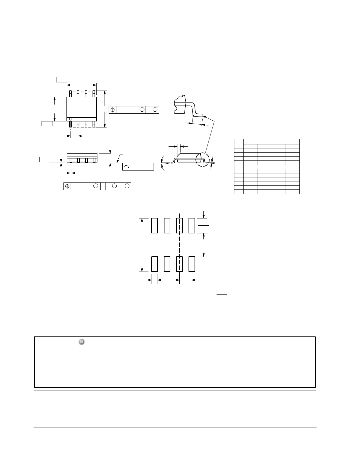
NCP1575
PACKAGE DIMENSIONS
SOIC−8
D SUFFIX
CASE 751−07
ISSUE AC
−Y−
−Z−
−X−
A
58
B
1
S
0.25 (0.010)
4
M
M
Y
K
G
C
SEATING
PLANE
0.10 (0.004)
H
D
0.25 (0.010) Z
M
SXS
Y
N
X 45
M
J
NOTES:
1. DIMENSIONING AND TOLERANCING PER
ANSI Y14.5M, 1982.
2. CONTROLLING DIMENSION: MILLIMETER.
3. DIMENSION A AND B DO NOT INCLUDE
MOLD PROTRUSION.
4. MAXIMUM MOLD PROTRUSION 0.15 (0.006)
PER SIDE.
5. DIMENSION D DOES NOT INCLUDE DAMBAR
PROTRUSION. ALLOWABLE DAMBAR
PROTRUSION SHALL BE 0.127 (0.005) TOTAL
IN EXCESS OF THE D DIMENSION AT
MAXIMUM MATERIAL CONDITION.
6. 751−01 THRU 751−06 ARE OBSOLETE. NEW
STANDARD IS 751−07.
MILLIMETERS
DIMAMIN MAX MIN MAX
4.80 5.00 0.189 0.197
B 3.80 4.00 0.150 0.157
C 1.35 1.75 0.053 0.069
D 0.33 0.51 0.013 0.020
G 1.27 BSC 0.050 BSC
H 0.10 0.25 0.004 0.010
J 0.19 0.25 0.007 0.010
K 0.40 1.27 0.016 0.050
M 0 8 0 8
N 0.25 0.50 0.010 0.020
S 5.80 6.20 0.228 0.244
INCHES
SOLDERING FOOTPRINT*
1.52
0.060
7.0
0.275
4.0
0.155
0.6
0.024
1.270
0.050
SCALE 6:1
mm
inches
*For additional information on our Pb−Free strategy and soldering
details, please download the ON Semiconductor Soldering and
Mounting Techniques Reference Manual, SOLDERRM/D.
V2 is a trademark of Switch Power, Inc.
ON Semiconductor and are registered trademarks of Semiconductor Components Industries, LLC (SCILLC). SCILLC reserves the right to make changes without further notice
to any products herein. SCILLC makes no warranty, representation or guarantee regarding the suitability of its products for any particular purpose, nor does SCILLC assume any liability
arising out of the application or use of any product or circuit, and specifically disclaims any and all liability, including without limitation special, consequential or incidental damages.
“Typical” parameters which may be provided in SCILLC data sheets and/or specifications can and do vary in different applications and actual performance may vary over time. All
operating parameters, including “Typicals” must be validated for each customer application by customer’s technical experts. SCILLC does not convey any license under its patent rights
nor the rights of others. SCILLC products are not designed, intended, or authorized for use as components in systems intended for surgical implant into the body, or other applications
intended to support or sustain life, or for any other application in which the failure of the SCILLC product could create a situation where personal injury or death may occur. Should
Buyer purchase or use SCILLC products for any such unintended or unauthorized application, Buyer shall indemnify and hold SCILLC and its officers, employees, subsidiaries, affiliates,
and distributors harmless against all claims, costs, damages, and expenses, and reasonable attorney fees arising out of, directly or indirectly, any claim of personal injury or death
associated with such unintended or unauthorized use, even if such claim alleges that SCILLC was negligent regarding the design or manufacture of the part. SCILLC is an Equal
Opportunity/Affirmative Action Employer. This literature is subject to all applicable copyright laws and is not for resale in any manner.
PUBLICATION ORDERING INFORMATION
LITERATURE FULFILLMENT:
Literature Distribution Center for ON Semiconductor
P.O. Box 61312, Phoenix, Arizona 85082−1312 USA
Phone: 480−829−7710 or 800−344−3860 Toll Free USA/Canada
Fax: 480−829−7709 or 800−344−3867 Toll Free USA/Canada
Email: [email protected]
N. American Technical Support: 800−282−9855 Toll Free
USA/Canada
Japan: ON Semiconductor, Japan Customer Focus Center
2−9−1 Kamimeguro, Meguro−ku, Tokyo, Japan 153−0051
Phone: 81−3−5773−3850
http://onsemi.com
ON Semiconductor Website: http://onsemi.com
Order Literature: http://www.onsemi.com/litorder
For additional information, please contact your
local Sales Representative.
NCP1575/D
16
 Loading...