

Page 1

NCP1232
Microprocessor Monitor
The NCP1232 is a fully–integrated processor supervisor. It provides
three important functions to safeguard processor functionality:
precision power on/off reset control, watchdog timer and external
reset override.
On power–up, the NCP1232 holds the processor in the reset state for
a minimum of 250 msec after VCC is within tolerance to ensure a
stable system start–up.
Microprocessor functionality is monitored by the on–board
watchdog circuit. The microprocessor must provide a periodic
low–going signal on the ST
this signal within the selected time–out period (150 msec, 600 msec or
1200 msec), an out–of–control processor is indicated and the
NCP1232 issues a processor reset as a result.
The outputs of the NCP1232 are immediately driven active when
the PB input is brought low by an external push–button switch or other
electronic signal. When connected to a push–button switch, the
NCP1232 provides contact debounce.
The NCP1232 is packaged in a space–saving 8–pin plastic SOIC
package and requires no external components.
input. Should the processor fail to supply
http://onsemi.com
SO–8
8
1
YY, Y = Year
WW = Work Week
X = Assembly ID Code
Z = Subcontractor ID Code
D SUFFIX
CASE 751
MARKING
DIAGRAM
8
NCP
1232
YWWXZ
1
Features
• Precision Voltage Monitor
(Adjustable +4.5 V or +4.75 V)
• Reset Pulse Width (250 msec Min)
• No External Components
• Adjustable Watchdog Timer
(150 msec, 600 msec or 1.2 sec)
• Debounced Manual Reset Input for External Override
Applications
• Computers
• Controllers
• Intelligent Instruments
• Automotive Systems
• Critical µP Power Monitoring
PIN CONNECTIONS
8–Pin SOIC
TD
TOL
1
2
3
4
(Top View)
PB RST
ORDERING INFORMATION
Device Package Shipping
NCP1232DR2 SO–8 2500 Tape & Reel
8
V
CC
7
ST
6
RST
NCP1232D
5
RSTGND
Semiconductor Components Industries, LLC, 2000
May, 2000 – Rev. 0
1 Publication Order Number:
NCP1232/D
Page 2
NCP1232
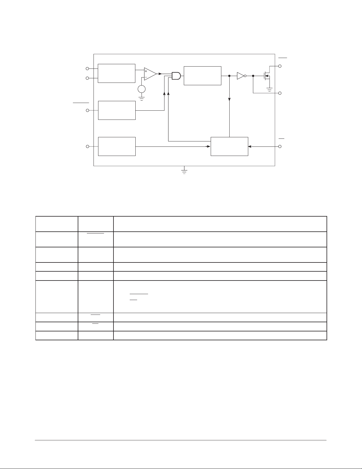
FUNCTIONAL BLOCK DIAGRAM
VD
CC
TOL
PB RST
TD
5%/10%
TOLERANCE
SELECT
DEBOUNCE
WATCHDOG
TIMEBASE
SELECT
REF
GND
RESET
GENERATOR
NCP1232
WATCHDOG
TIMER
RST
RST
ST
PIN DESCRIPTION
Pin No.
(8–Pin SOIC)
1 PB RST Push–button Reset Input. A debounced active–low input that ignores pulses less than 1 msec in
2 TD Time Delay Set. The watchdog time–out select input (tTD = 150 msec for
3 TOL Tolerance Input. Connect to GND for 5% tolerance or to VCC for 10% tolerance.
4 GND Ground.
5 RST Reset Output (Active High) – goes active:
6 RST Reset Output (Active Low, Open Drain) – see RST.
7 ST Strobe Input. Input for watchdog timer.
8 V
Symbol Description
duration and is guaranteed to recognize inputs of 20 msec or greater.
TD = 0 V, tTD = 600 msec for TD = open, tTD = 1.2 sec for TD = VCC.)
CC
1. If VCC falls below the selected reset voltage threshold
2. If PB RST
3. If ST
4. During power–up
The +5 V Power Supply Input.
is forced low
is not strobed within the minimum time–out period
http://onsemi.com
2
Page 3
NCP1232
ABSOLUTE MAXIMUM RATINGS* Voltage on any pin (with respect to GND) –0.3 V to +5.8 V
Rating
Operating Temperature Range –40 to +85 °C
Storage Temperature Range, T
Lead Temperature (Soldering, 10 sec) +300 °C
*Stresses beyond those listed under “Absolute Maximum Ratings’’ may cause permanent damage to the device. These are stress ratings only ,
and functional operation of the device at these or any other conditions beyond those indicated in the operational sections of the specifications
is not implied. Exposure to absolute maximum rating conditions for extended periods may affect device reliability .
stg
Value Unit
–65 to +150
°C
DC ELECTRICAL CHARACTERISTICS (T
Characteristic
Supply Voltage V
ST and PB RST Input High Level V
ST and PB RST Input Low Level V
Input Leakage ST, TOL I
Output Current RST I
Current RST, RST I
Operating Current I
VCC 5% Trip Point (Note 3.) V
VCC 10% Trip Point (Note 3.) V
CAPACITANCE (Note 4.) (T
Characteristic
Input Capacitance ST, TOL C
Output Capacitance RST, RST C
= +25°C)
A
AC ELECTRICAL CHARACTERISTICS (T
Characteristic
PB RST (Note 5.) t
PB RST Delay t
Reset Active Time t
ST Pulse Width t
ST Time–out Period t
VCC Fall Time (Note 4.) t
VCC Rise Time (Note 4.) t
VCC Detect to RST High and RST Low t
VCC Detect to RST High and RST Open
(Note 6.)
1. PB RST is internally pulled up to VCC with an internal impedance of typically 40 kΩ.
2. Measured with outputs open.
3. All voltages references to GND.
4. Guaranteed by design.
5. PB RST
6. tR = 5 µsec.
must be held low for a minimum of 20 msec to guarantee a reset.
= T
A
A
to T
MIN
Symbol Test Conditions Min Typ Max Unit
CC
IH
IL
L
OH
OL
CC
CCTP
CCTP
Symbol Test Conditions Min Typ Max Unit
IN
OUT
= T
to T
MIN
Symbol Test Conditions Min Typ Max Unit
PB
PBD
RST
ST
TD
F
R
RPD
t
RPU
; VCC = +4.5 V to 5.5 V, unless otherwise specified.)
MAX
– 4.5 5.0 5.5 V
Note 1. 2.0 – VCC +0.3 V
– –0.3 – +0.8 V
– –1.0 – +1.0 µA
VOH = 2.4 V –1.0 –12 – mA
VOL = 0.4 V 2.0 10 – mA
Note 2. – 50 200 µA
TOL = GND 4.50 4.62 4.74 V
TOL = V
; VCC = +5.0 V to "10%, unless otherwise specified.)
MAX
TD Pin = 0 V
TD Pin = Open
TD Pin = V
Figure 7, VCC Falling – – 100 nsec
Figure 8, VCC Rising 250 610 1000 msec
CC
– – – 5.0 pF
– – – 7.0 pF
Figure 3 20 – – msec
Figure 3 1.0 4.0 20 msec
– 250 610 1000 msec
Figure 4 20 – – nsec
Figure 4
CC
Figure 5 10 – – µsec
Figure 6 0 – – µsec
4.25 4.37 4.49 V
62.5
250
500
150
600
1200
250
1000
2000
msec
http://onsemi.com
3
Page 4

NCP1232
Power Monitor
The NCP1232 detects out–of–tolerance power supply
conditions and warns a processor–based system of an
impending power failure. When VCC is detected as below
the preset level defined by TOL, the VCC comparator
outputs the signals RST and RST
. If TOL is connected to
ground, the RST and RST signals become active as VCC falls
below 4.75 volts. If TOL is connected to VCC, the RST and
RST
become active as VCC falls below 4.5 volts. Because
the processing is stopped at the last possible moment of valid
VCC, the RST and RST are excellent control signals for a µP.
The reset outputs will remain in their active states until V
CC
has been continuously in–tolerance for a minimum of 250
msec allowing the power supply and µP to stabilize before
RST
is released.
Push–button Reset Input
The debounced manual reset input (PB RST) manually
forces the reset outputs into their active states. Once PB RST
has been low for a time, t
, the push–button delay time,
PBD
the reset outputs go active. The reset outputs remain in their
active states for a minimum of 250 msec after PB RST
rises
above VIH (Figure 3).
A mechanical push–button or active logic signal can drive
the PB RST input. The debounced input ignores input pulses
less than 1 msec and is guaranteed to recognize pulses of
20 msec or greater. No external pull–up resistor is required
because the PB RST
input has an internal pull–up to VCC of
approximately 100 µA.
Watchdog Timer
When the ST input is not stimulated for a preset time
period, the watchdog timer function forces RST and RST
signals to the active state. The preset time period is
determined by the TD inputs to be 150 msec with TD
connected to ground, 600 msec with TD open, or 1200 msec
with TD connected to VCC, typical. The watchdog timer
starts timing out from the set time period as soon as RST and
RST
are inactive. If a high–to–low transition occurs on the
ST input pin prior to time–out, the watchdog timer is reset
and begins to time–out again. If the watchdog timer is
allowed to time–out, then the RST and RST signals are
driven to the active state for 250 msec minimum (Figure 2).
The software routine that strobes ST
is critical. The code
must be in a section of software that is executed regularly so
the time between toggles is less than the watchdog time–out
period. One common technique controls the µP I/O line
from two sections of the program. The software might set the
I/O line high while operating in the foreground mode and set
it low while in the background or interrupt mode. If both
modes do not execute correctly, the watchdog timer issues
reset pulses.
Supply Monitor Noise Sensitivity
The NCP1232 is optimized for fast response to
negative–going changes in VDD. Systems with an inordinate
amount of electrical noise on VDD (such as systems using
relays), may require a 0.01 µF or 0.1 µF bypass capacitor to
reduce detection sensitivity. This capacitor should be
installed as close to the NCP1232 as possible to keep the
capacitor lead length short.
+5 V
3–TERMINAL
REGULATOR
V
CC
PB RST
GND
Figure 1. Push–button Reset
+5 V
0.1 µF
Figure 2. Watchdog Timer
NCP1232
TOL
V
CC
NCP1232
TD
TD
ST
RST
TOL
I/O
MICRO–
PROCESSOR
RESET
+5 V
RST
ST
GND
10 KΩ
RESET
MICRO–
PROCESSOR
I/O
http://onsemi.com
4
Page 5

NCP1232
t
PB
PB RST
RST
RST
t
PBD
V
IH
V
IL
t
RST
Figure 3. Push–button Reset. The debounced PB RST
input ignores input pulses less than 1 msec and is
guaranteed to recognized pulses of 20 msec or greater
PUSH–BUTTON RESET
t
ST
ST
t
TD
Figure 4. Strobe Input
NOTE: tTD is the maximum elapsed time between ST
transistions (ST is activated by falling edges only) which will
keep the watchdog timer from forcing the reset outputs active
for a time of t
as tabulated below.
CONDITION MIN TYP
TD PIN = 0 V 62.5 msec 150 msec 250 msec
TD PIN = OPEN 250 msec 600 msec 1000 msec
TD PIN = V
CC
. tTD is a function of the voltage at the TD pin,
RST
t
500 msec 1200 msec 2000 msec
high–to–low
TD
MAX
http://onsemi.com
5
Page 6

NCP1232
t
F
V
CC
+4.75 V
+4.25 V
V
CC
t
R
+4.25 V
+4.75 V
Figure 5. Power–Down Slew Rate
VCC = 5 V
+4.5 V (5% TRIP POINT)
+4.25 V (10% TRIP POINT)
t
RPD
RST
V
OH
RST
VCC, SLEW RATE = 1.66mV/µsec (0.5 V/300 µsec)
V
OL
Figure 6. Power–Down Slew Rate
4.5 V (10% TRIP POINT)
V
CC
RST
RST
4.6 V (5% TRIP POINT)
t
RPU
V
OH
V
OL
Figure 7. VCC Detect Reset Output Delay
(Power–Down)
Figure 8. VCC Detect Reset Output Delay
(Power–Up)
http://onsemi.com
6
Page 7

NCP1232
P ACKAGE DIMENSIONS
SO–8
D SUFFIX
CASE 751–06
ISSUE T
C
A
A1
D
58
0.25MB
E
1
B
e
H
4
M
h
X 45
_
q
C
A
SEATING
PLANE
0.10
L
B
SS
A0.25MCB
NOTES:
1. DIMENSIONING AND TOLERANCING PER ASME
Y14.5M, 1994.
2. DIMENSIONS ARE IN MILLIMETER.
3. DIMENSION D AND E DO NOT INCLUDE MOLD
PROTRUSION.
4. MAXIMUM MOLD PROTRUSION 0.15 PER SIDE.
5. DIMENSION B DOES NOT INCLUDE DAMBAR
PROTRUSION. ALLOWABLE DAMBAR
PROTRUSION SHALL BE 0.127 TOTAL IN EXCESS
OF THE B DIMENSION AT MAXIMUM MATERIAL
CONDITION.
MILLIMETERS
DIM MIN MAX
A 1.35 1.75
A1 0.10 0.25
B 0.35 0.49
C 0.19 0.25
D 4.80 5.00
E
3.80 4.00
1.27 BSCe
H 5.80 6.20
h
0.25 0.50
L 0.40 1.25
0 7
q
__
http://onsemi.com
7
Page 8

NCP1232
ON Semiconductor and are trademarks of Semiconductor Components Industries, LLC (SCILLC). SCILLC reserves the right to make changes
without further notice to any products herein. SCILLC makes no warranty , representation or guarantee regarding the suitability of its products for any particular
purpose, nor does SCILLC assume any liability arising out of the application or use of any product or circuit, and specifically disclaims any and all liability ,
including without limitation special, consequential or incidental damages. “Typical” parameters which may be provided in SCILLC data sheets and/or
specifications can and do vary in different applications and actual performance may vary over time. All operating parameters, including “Typicals” must be
validated for each customer application by customer’s technical experts. SCILLC does not convey any license under its patent rights nor the rights of others.
SCILLC products are not designed, intended, or authorized for use as components in systems intended for surgical implant into the body, or other applications
intended to support or sustain life, or for any other application in which the failure of the SCILLC product could create a situation where personal injury or
death may occur. Should Buyer purchase or use SCILLC products for any such unintended or unauthorized application, Buyer shall indemnify and hold
SCILLC and its officers, employees, subsidiaries, affiliates, and distributors harmless against all claims, costs, damages, and expenses, and reasonable
attorney fees arising out of, directly or indirectly , any claim of personal injury or death associated with such unintended or unauthorized use, even if such claim
alleges that SCILLC was negligent regarding the design or manufacture of the part. SCILLC is an Equal Opportunity/Affirmative Action Employer .
PUBLICATION ORDERING INFORMATION
NORTH AMERICA Literature Fulfillment:
Literature Distribution Center for ON Semiconductor
P.O. Box 5163, Denver, Colorado 80217 USA
Phone: 303–675–2175 or 800–344–3860 Toll Free USA/Canada
Fax: 303–675–2176 or 800–344–3867 Toll Free USA/Canada
Email: ONlit@hibbertco.com
Fax Response Line: 303–675–2167 or 800–344–3810 T oll Free USA/Canada
N. American Technical Support: 800–282–9855 Toll Free USA/Canada
EUROPE: LDC for ON Semiconductor – European Support
German Phone : (+1) 303–308–7140 (M–F 1:00pm to 5:00pm Munich T ime)
Email: ONlit–german@hibbertco.com
French Phone: (+1) 303–308–7141 (M–F 1:00pm to 5:00pm Toulouse Time)
Email: ONlit–french@hibbertco.com
English Phone: (+1) 303–308–7142 (M–F 12:00pm to 5:00pm UK Time)
Email: ONlit@hibbertco.com
EUROPEAN TOLL–FREE ACCESS*: 00–800–4422–3781
*Available from Germany, France, Italy, England, Ireland
CENTRAL/SOUTH AMERICA:
Spanish Phone: 303–308–7143 (Mon–Fri 8:00am to 5:00pm MST)
Email: ONlit–spanish@hibbertco.com
ASIA/PACIFIC : LDC for ON Semiconductor – Asia Support
Phone: 303–675–2121 (Tue–Fri 9:00am to 1:00pm, Hong Kong T ime)
T oll Free from Hong Kong & Singapore:
001–800–4422–3781
Email: ONlit–asia@hibbertco.com
JAPAN: ON Semiconductor, Japan Customer Focus Center
4–32–1 Nishi–Gotanda, Shinagawa–ku, T okyo, Japan 141–0031
Phone: 81–3–5740–2745
Email: r14525@onsemi.com
ON Semiconductor Website: http://onsemi.com
For additional information, please contact your local
Sales Representative.
http://onsemi.com
8
NCP1232/D
 Loading...