

Page 1
NCP1205
Single Ended PWM
Controller Featuring QR
Operation and Soft
Frequency Foldback
The NCP1205 combines a true Current Mode Control modulator
and a demagnetization detector to ensure full Discontinuous
Conduction Mode in any load/line conditions and minimum drain
voltage switching (Quasi–Resonant operation, also called critical
conduction operation). With its inherent Variable Frequency Mode
(VFM), the controller decreases its operating frequency at constant
peak current whenever the output power demand diminishes.
Associated with automatic multiple valley switching, this unique
architecture guarantees minimum switching losses and the lowest
power drawn from the mains when operating at no–load conditions.
Thus, the NCP1205 is optimal for applications targeting the newest
International Energy Agency (IEA) recommendations for standby
power.
The internal High–Voltage current source provides a reliable
charging path for the VCC capacitor and ensures a clean and short
start–up sequence without deteriorating the efficiency once off.
The continuous feedback signal monitoring implemented with an
Over–Current fault Protection circuitry (OCP) makes the final design
rugged and reliable. An internal Over Voltage Protection (OVP) circuit
continuously monitors the VCC pin and stops the IC whenever its level
exceeds 36 V. The DIP14 offers an adjustable version of the OVP
threshold via an external resistive network.
Features
• Natural Drain Valley Switching for Lower EMI and Quasi–Resonant
Operation (QR)
• Smooth Frequency Foldback for Low Standby and Minimum Ripple
at Light–Load
• Adjustable Maximum Switching Frequency
• Internal 200 ns Leading Edge Blanking on Current Sense
• 250 mA Sink and Source Driver
• Wide Operating Voltages: 8.0 to 36 V
• Wide UVLO Levels: 7.2 to 15 V Typical
• Auto–Recovery Internal Short–Circuit Protection (OCP)
• Integrated 3.0 mA Typ. Start–Up Source
• Current Mode Control
• Adjustable Over–Voltage Level
• Available in DIP8 and DIP14 Package
http://onsemi.com
MARKING
DIAGRAMS
8
1
1
14
NCP1205P2
1
NCP1205P
YYWW
AWLYYWW
PDIP–8
8
1
14
1
ORDERING INFORMATION
Device Package Shipping
NCP1205P PDIP–8 50 Units/Rail
NCP1205P2 PDIP–14 25 Units/Rail
N SUFFIX
CASE 626
PDIP–14
P SUFFIX
CASE 646
A = Assembly Location
WL = Wafer Lot
YY = Year
WW = Work Week
AWL
Applications
• High Power AC/DC Adapters for Notebooks, etc.
• Offline Battery Chargers
• Power Supplies for DVD, CD Players, TVs, Set–Top Boxes, etc.
• Auxiliary Power Supplies (USB, Appliances, etc.)
Semiconductor Components Industries, LLC, 2002
April, 2002 – Rev. 2
1 Publication Order Number:
NCP1205/D
Page 2
NCP1205
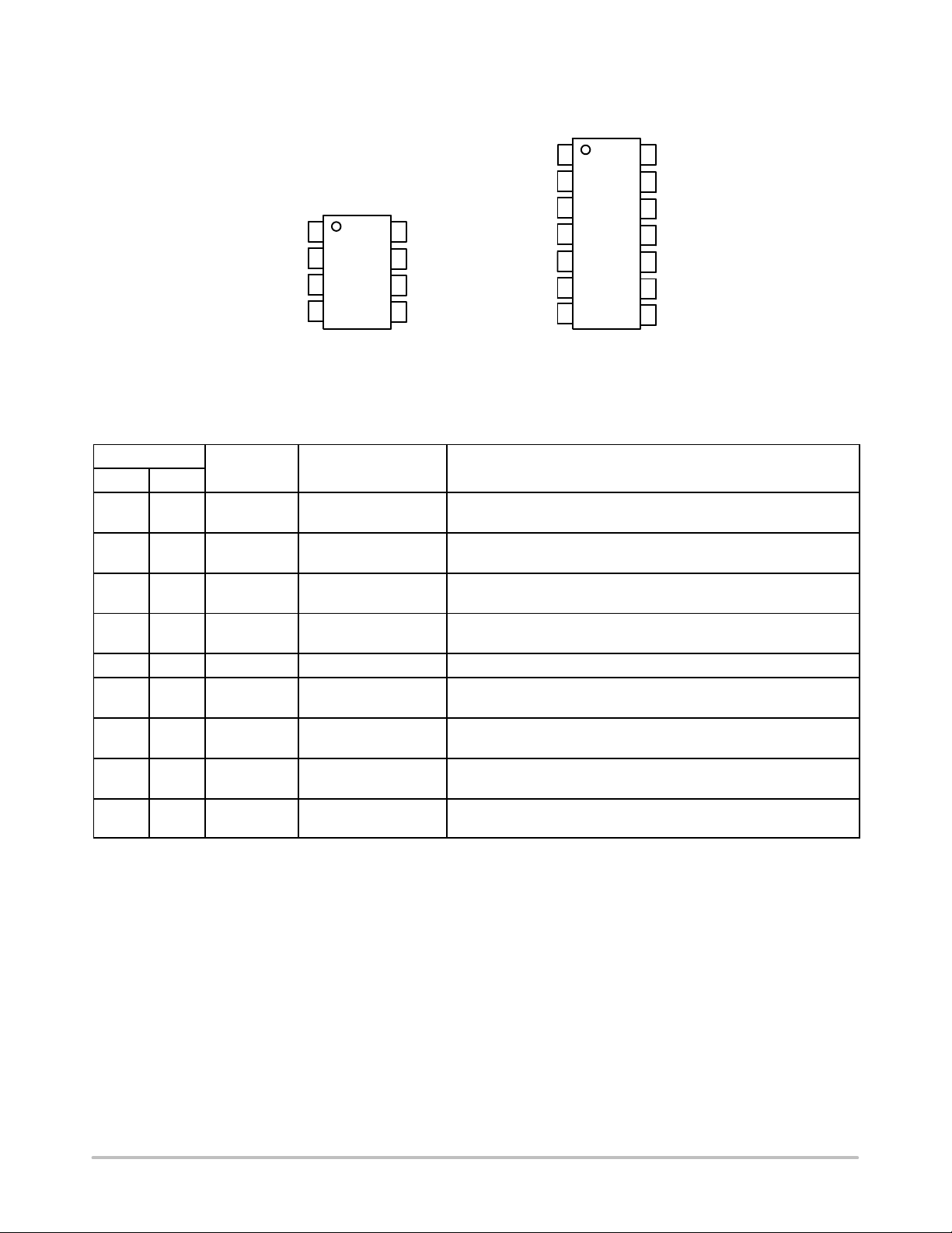
PIN CONNECTIONS
HV
Demag
FB
Ct
1
2
3
4
PDIP–8
8
7
6
5
V
CC
Drive
Isense
GND
HV
NC
Demag
FB
Ct
OVP
NC
1
2
3
4
5
6
7
PDIP–14
14
13
12
11
10
9
8
NC
V
CC
Drive
Isense
GND
NC
NC
PIN FUNCTION DESCRIPTION
Pin No.
DIP8 DIP14
1 1 HV Start–up rail Connected to the rectified HV rail, this pin provides a charging path to
2 3 Demag Zero primary–current
3 4 FB Feedback signal to
4 5 Ct Timing capacitor By adding a capacitor from Ct to the ground, the user selects the
5 10 Gnd The IC’s ground –
NA 6 OVP Overvoltage input By applying a 2.8 V typical level on this pin, the IC is permanently
6 11 Isense The primary–current
7 12 Drv This pin drives the
8 13 V
1. DIP14 has different pinouts. Please see Pin Connections.
2. Pin 2, 7, 8, 9 and 14 are nonconnected on DIP14.
Pin Name Function Description
V
bulk capacitor.
CC
This pin ensures the re–start of the main switcher when operating in
detection
free–run.
This level modulates the peak current level in free–running operation
control the PWM
and modulates the frequency in VFM operation.
minimum/maximum operating frequency.
latched–off until V
falls below UVLOL.
CC
This pin senses the primary current via an external shunt resistor.
sensing pin
The IC is able to deliver or absorb 250 mA peak currents while
CC
external switcher
Powers the IC A positive voltage up to 40 V
delivering a clamped driving signal.
typical
can be applied upon this pin
before the IC stops.
http://onsemi.com
2
Page 3
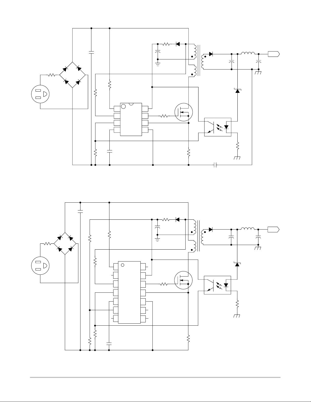
4x1N4007
R5
15
Universal Input
+
C1
10 µF
R8
22 k
* R10
15 k
1
2
NCP1205P
3
4
NCP1205
R2
150
+
C14
22 µF
8
7
6
5
R4
10
D2
1N4148
M2
MTD1N60E
D6
1N5819
IC4
C10
470 µF
10 V
D7
5.1 V
L2
10 µH
++
C11
100 µF
10 V
5 V
4x1N4007
R5
15
Universal Input
C12
R6
1 nF
4.7 k
* Please refer to the application information section regarding this element.
R3
3.3
Figure 1. Typical Application Example for DIP8 Version
+
C1
10 µF
R8
22 k
* R10
15 k
NCP1205P2
1 14
2
3
4
5
6
7
13
12
11
10
9
8
D2
R2
1N4148
15
+
C14
33 µF/35 V
M2
MTD1N60E
R4
6.8
SFH6156–2
C13
1.5 nF Y1
D6
1N5819
C10
470 µF
10 V
IC4
SFH6156–2
R1
560
L2
10 µH
D7
4.3 V
R1
560
++
C11
47 µF
10 V
5 V
R6
2.7 k
C12
ROVPL ROVPU
* Please refer to the application information section regarding this element.
1 nF
Figure 2. Typical Application Example for DIP14 Version
http://onsemi.com
3
R3
3.3
Page 4
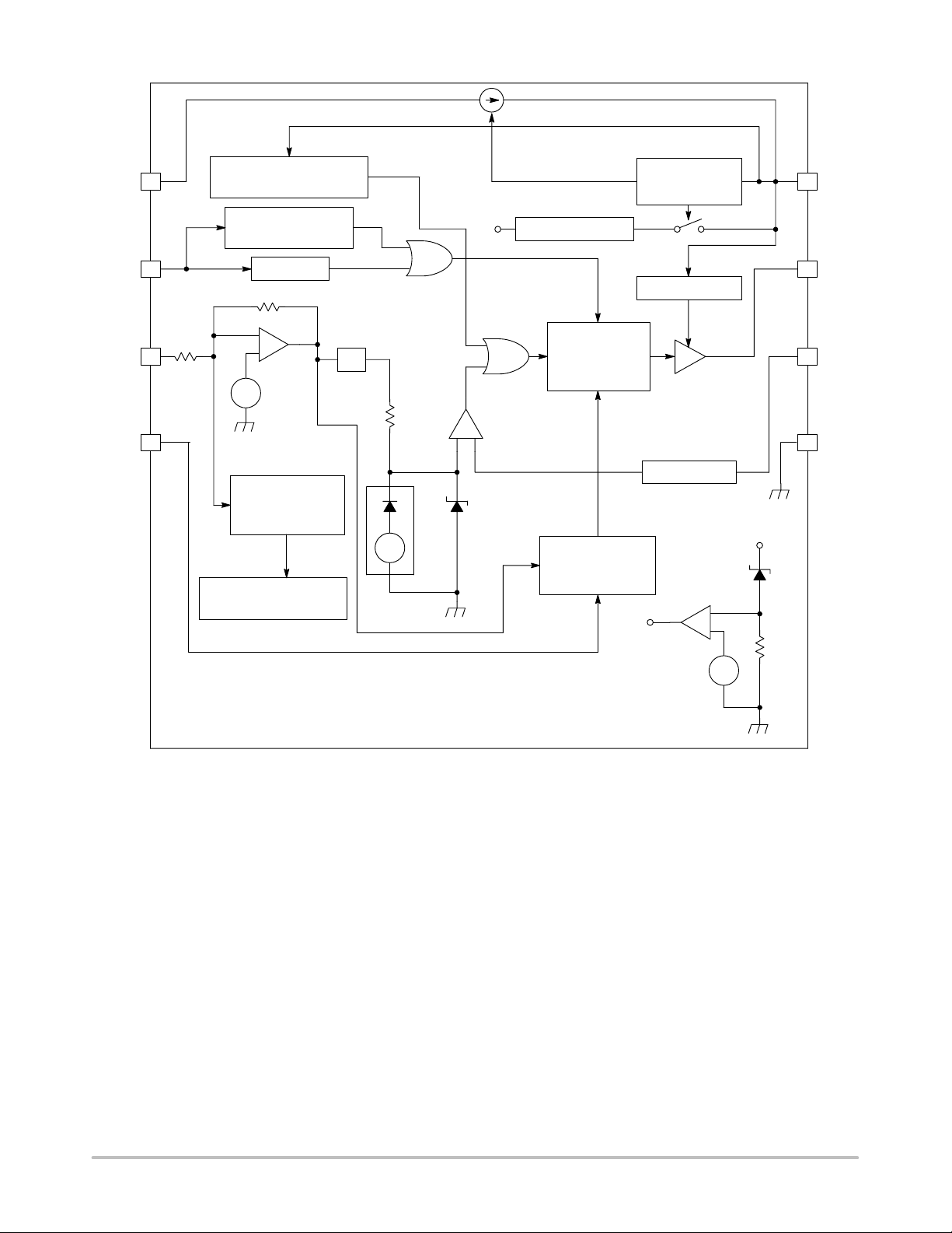
NCP1205
Startup
HV
Demag
FB
Ct
1
2
Protection (V
> 40 V)
CC
Last Pulse of Demag
after 4 µs
DEMAG ?
Internal V
CC
Internal Regulator
Rf
V
Max = 3 V
err
V
Min = 10 mV
Over Voltage
Ri
3
–
+
+
2.5 V
–
4 5
err
1/3
Current Comparator
–
+
250 mV – 1 V
Max Setpoint
Clock
Flip–Flop
RQ
D
UVLO
= 15 V
H
UVLO
= 7.2 V
L
Internal Clamp
Driver
200 ns L.E.B
Over Current
Protection (OCP)
V(–) < 1.5 V
+
–
Lasts more than 128 ms?
––> Protection Circuitry
1 V
250 mV Clamp
V
Pin 8
CC
err
VCO Feedback
T
= f (V
off
err
= f (Ct)
Max T
off
)
35 V Zener
V
+
OVP
–
18 k
+
2.8 V
–
8
V
CC
7
DRV
6
I
sense
Gnd
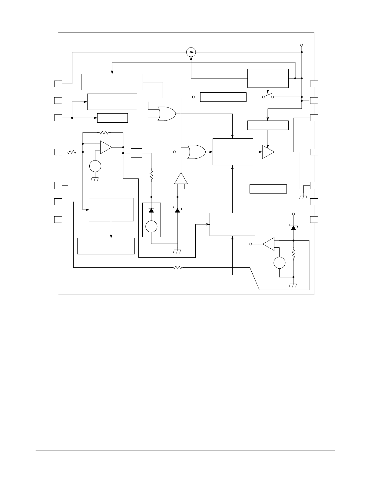
Figure 3. Internal Circuit Architecture for DIP8 Version
http://onsemi.com
4
Page 5
HV
NC
NCP1205
V
Pin 13
CC
Startup
UVLO
= 15 V
1
2
Protection (V
Last Pulse of Demag
after 4 µs
> 40 V)
CC
Internal V
CC
Internal Regulator
Over Voltage
UVLO
H
= 7.2 V
L
14
13
V
CC
Demag
FB
OVP
NC
Ct
3
Ri
4
5
6
7
Lasts more than 128 ms?
––> Protection Circuitry
DEMAG ?
Rf
–
+
+
2.5 V
–
Over Current
Protection (OCP)
V(–) < 1.5 V
Max = 3 V
V
err
V
Min = 10 mV
err
1/3
+
–
OVP
Current Comparator
–
+
250 mV – 1 V
Max Setpoint
1 V
250 mV Clamp
2.0 k
Internal Clamp
Clock
Flip–Flop
RQ
D
Driver
200 ns L.E.B
V
Pin 13
CC
err
VCO Feedback
T
= f (V
off
err
= f (Ct)
Max T
off
)
35 V Zener
V
+
OVP
–
18 k
+
2.8 V
–
12
11
10
DRV
I
sense
Gnd
NC
9
NC
8
Figure 4. Internal Circuit Architecture for DIP14 Version
http://onsemi.com
5
Page 6

NCP1205
MAXIMUM RATINGS
Pin No.
Rating
Power Supply Voltage 8 13 V
Thermal Resistance Junction–to–Air DIP8
DIP14
Operating Junction Temperature Range
Maximum Junction Temperature
Storage Temperature Range – – T
ESD Capability, HBM Model All Pins All Pins
ESD Capability, Machine Model All Pins All Pins
DIP8 DIP14
–
–
–
–
–
–
–
–
Symbol
in
R
JA
T
J
T
Jmax
stg
–
–
Demagnetization Pin Current 3 3 – – 5.0 mA
Value
Min Max
– 45 V
–
–
–
–
100
100
–25 to +125
150
– –60 to +150 °C
– 2.0 kV
– 200 V
Unit
°C/W
°C
°C
ELECTRICAL CHARACTERISTICS (For typical values T
V
= 12 V unless otherwise noted.)
CC
= 25°C, for min/max values TJ = –25°C to +125°C, Max TJ = 150°C,
A
Pin No.
Characteristics
DIP8 DIP14
Symbol Min Typ Max Unit
Demagnetization Block
Input Threshold Voltage (V
Hysteresis (V
decreasing) 2 3 V
pin2
Input Clamp Voltage
High State (I
Low State (I
= 3.0 mA)
pin2
= –3.0 mA)
pin2
increasing) 2 3 Vth 50 65 85 mV
pin2
H
– 30 – mV
2 3
VC
VC
H
L
8.0
–0.9
10
–0.7
12
–0.5
Demag Propagation Delay – – – 100 300 350 ns
No Demag Signal Activation – – – – 4.0 8.0 µs
Internal Input Capacitance at 1.0 V 2 3 C
pin2
– 10 – pF
Demag Propagation Delay with 22 kΩ External Resistor 2 3 – 100 370 480 ns
Feedback Path
Input Impedance at V
Internal Error Amplifier Closed Loop Gain 3 4 AV
Internal Built–In Offset Voltage for Error Detection – – V
= 3.0 V 3 4 Zin – 50 – kΩ
FB
CL
ref
– –3.0 – –
2.2 2.5 2.8 V
Error Amplifier Level of VCO Take Over – – – – 1.0 – V
Internal Divider from Internal Error Amp, Pin to Current
– – – – 3.0 – –
Setpoint
V
Fault Detection Circuitry
Internal Over Current Level
– – WL
L
– 1.5 – V
Fault Time Duration to Latch Activation @ Ct = 1.0 ηF – – – – 128 – ms
Over Current Latch–Off Phase @ Ct = 1.0 ηF – – – – 1.0 – s
Hysteresis when VFB goes back into Regulation – – – – 100 – mV
VCC (Pin 8) Over Voltage Protection 8 13 OVP1 36 40 43 V
Over Voltage Protection Threshold for DIP14 Version 6 6 OVP2 2.5 2.8 3.1 V
Current Sense Comparator
Input Bias Current @ 1.0 V
Maximum Current Setpoint 6 11 V
Minimum Current Setpoint 6 11 V
6 11 I
IB
min
– 0.02 – µA
cl
0.9 1.0 1.1 V
225 250 285 mV
http://onsemi.com
6
Page 7

NCP1205
ELECTRICAL CHARACTERISTICS (continued) (For typical values T
Max T
= 150°C, VCC = 12 V unless otherwise noted.)
J
= 25°C, for min/max values TJ = 25°C to +125°C,
A
Pin No.
Characteristics
DIP8 DIP14
Symbol Min Typ Max Unit
Current Sense Comparator (continued)
Propagation Delay from Current Detection to Gate OFF
6 11 T
del
– 200 250 ns
State
Leading Edge Blanking (LEB) 6 11 T
leb
– 200 – ns
Frequency Modulator
Minimum Frequency Operation @ Ct = 1.0 ηF and
V
= 35 V
CC
Maximum Frequency Operation @ Ct = 1.0 ηF and
V
= 35 V
CC
4 5 F
4 5 F
min
max
– 0 – kHz
90 110 125 kHz
Minimum Ct Charging Current (Note 3) 4 5 ICtmin – 0 – µA
Maximum Ct Charging Current (Note 3) 4 5 ICtmax 280 350 420 µA
Discharge Time @ Ct = 1.0 ηF 4 5 – – 500 – ns
Drive Output
Output Voltage Rise Time @ C
Output Voltage Fall Time @ CL = 1.0 ηF (V = 10 V) 7 12 t
Clamped Output Voltage @ VCC = 35 V (Note 4) 7 12 V
Voltage Drop on the Stage @ VCC = 10 V (Note 4) 12 12 V
= 1.0 ηF (V = 10 V) 7 12 t
L
r
f
DRV
DRV
– 30 50 ns
– 30 50 ns
11 13 16 V
– – 0.5 V
Undervoltage Lockout
Startup Threshold (V
Minimum Operating Voltage (VCC Decreasing) 8 13 UVLO
Increasing) 8 13 UVLO
CC
13.5 15 16.5 V
H
6.5 7.2 8.0 V
L
Startup Current Source
Maximum Voltage, Pin 1 Grounded
1 1 – – 450 – V
Maximum Voltage, Pin 1 Decoupled (470 µF) 1 1 – – 500 – V
Startup Current Source Flowing through Pin 1 1 1 – 2.3 3.0 4.8 mA
Leakage Current in Offstate @ Vpin 1 = 500 V 1 1 – – 32 70 µA
Device Current Consumption
V
less than UVLO
CC
H
8 13 – – 1.5 1.8 mA
VCC = 35 V and Fsw = 2.0 kHz, CL = 1.0 ηF 8 13 – – 1.2 3.0 mA
VCC = 35 V and Fsw = 125 kHz, CL = 1.0 ηF 8 13 – – 3.0 4.0 mA
Startup Current to VCC Capacitor 8 13 – 1.4 – – mA
3. Typical capacitor swing is between 0.5 V and 3.5 V.
4. Guaranteed by design, T
= 25°C.
J
http://onsemi.com
7
Page 8

NCP1205
380
360
340
320
300
Ct CHARGING CURRENT (µA)
280
16.5
15.5
420
400
16
–50
0 50 100 –50 0 50 100150
TEMPERATURE (°C)
Figure 5. Ct Charging Current versus
Temperature
125
120
115
110
105
100
95
SWITCHING FREQUENCY (kHz)
90
TEMPERATURE (°C)
Figure 6. Switching Frequency @ Ct = 1 nF
versus Temperature
1100
1050
150
15
14.5
START–UP THRESHOLD (V)
14
13.5
–50 0 50 100 –50 0 50 100
TEMPERATURE (°C)
150
Figure 7. Start–up Threshold versus
Temperature
43
42
41
40
39
OVER VOLTAGE (V)
38
CC
V
37
36
–50 0 50 100 –50 0 50 100
TEMPERATURE (°C)
150
1000
950
MAXIMUM CURRENT SET POINT (mV)
900
TEMPERATURE (°C)
Figure 8. Maximum Current Set Point versus
Temperature
8
7.75
7.5
7.25
7
6.75
MINIMUM OPERATING VOLTAGE (V)
6.5
TEMPERATURE (°C)
150
150
Figure 9. VCC Over Voltage Protection versus
Temperature
http://onsemi.com
Figure 10. Minimum Operating Voltage versus
Temperature
8
Page 9

NCP1205
APPLICATION INFORMATION
Introduction
By implementing a unique smooth frequency reduction
technique, the NCP1205 represents a major leap toward
low–power Switch–Mode Power Supply (SMPS) integrated
management. The circuit combines free–running operation
with minimum drain–source switching (so–called valley
switching), which naturally reduces the peak current stress
as well as the ElectroMagnetic Interferences (EMI). At
I
L
Not 0 at
Turn ON
I
P
OFF
I
L(avg)
ON
nominal output power, the circuit implements a traditional
current–mode SMPS whose peak current setpoint is given
by the feedback signal. However, rather than keeping the
switching frequency constant, each cycle is initiated by the
end of the primary demagnetization. The system therefore
operates at the boundary between Discontinuous
Conduction Mode (DCM) and Continuous Conduction
Mode (CCM). Figure 11 details this terminology:
L > Lc
0
L = Lc
L < Lc
Borderline
D/Fs
Time
Figure 11. Defining the Conduction Mode, Discontinuous, Continuous and Borderline
When the output power demands decreases, the natural
switching frequency raises. As a natural result, switching
losses also increase and degrade the SMPS efficiency. To
overcome this problem, the maximum switching frequency
of the NCP1205 is clamped to typically 125 kHz. When the
free running mode (also called Borderline Control Mode,
BCM) reaches this clamp value, an internal
Voltage–Controlled Oscillator (VCO) takes over and starts
to decrease the switching frequency: we are in Variable
Frequency Mode (VFM). Please note that during this
transition phase, the peak current is not fixed but is still
decreasing because the output power demand does. At a
given state, the peak current reaches a minimum ceil
(typically 250 mV/Rsense), and cannot go further down: the
switching frequency continues its decrease down to a
possible minimum of 0 Hz (the IC simply stops switching).
During normal free–running operation and VFM, the
controller always ensures single or multiple drain–source
0 Before
Turn ON
0
Dead–Time
valley switching. We will see later on how this is internally
implemented.
The FLYBACK operation is mainly defined through a
simple formula:
Pout
1
·Lp·Ip2· Fsw (eq. 1)
2
With:
Lp the primary transformer inductance (also called the
magnetizing inductance)
Ip the peak current at which the MOSFET is turned off
Fsw the nominal switching frequency
To adjust the transmitted power, the PWM controller can
play on the switching frequency or the peak current setpoint.
To refine the control, the NCP1205 of fers the ability to play
on both parameters either altogether on an individual basis.
http://onsemi.com
9
Page 10

NCP1205
In order to clarify the device behavior, we can distinguish the
following simplified operating phases:
1. The load is at its nominal value. The SMPS operates in
borderline conduction mode and the switching
frequency is imposed by the external elements (Vin,
Lp, Ip, Vout). The MOSFET is turned on at the
minimum drain–source level.
2. The load starts to decrease and the free–running
frequency hits the internal clamp.
3. The frequency can no longer naturally increase
because of the clamp. The frequency is now controlled
by the internal VCO but remains constant. The peak
current finds no other option that diminishing to satisfy
equation (1).
4. The peak current has reached the internal minimum
ceiling level and is now frozen for the remaining
cycles.
5. To further reduce the transmitted power (V
the VCO decreases the switching frequency. In case of
output overshoot, the VCO could decrease the
frequency down to zero. When the overshoot has gone,
V
diminishes again and the IC smoothly resumes its
FB
operation.
Advantages of the Method
By implementing the aforementioned control scheme, the
NCP1205 brings the following advantages:
goes up),
FB
• Discontinuous only operation: in DCM, the Flyback is
a first order system (at low frequencies) and thus
naturally eases the feedback loop compensation.
• A low–cost secondary rectifier can be used due to
smooth turn–off conditions.
• Valley switching ensures minimum switching losses
brought by Coss and all the parasitic capacitances.
• By folding back the switching frequency, you turn the
system into Pulse Duration Modulation. This method
prevents from generating uncontrolled output ripple as
with hysteretic controllers.
• By letting you control the peak current value at which
the frequency goes down, you ensure that this level is
low enough to avoid transformer acoustic noise
generation even at audible frequencies.
Detailed Description
The following sections describe the internal behavior of
the NCP1205.
Free–Running Operation
As previously s aid, t he o perating f requency a t n ominal l oad
is dictated b y t he e xternal e lements. We can split the d if ferent
switching sections in t wo s eparated i nstants. I n t he following
text we use the internal error voltage, Verr. This level is
elaborated as F igure 1 4 p ortrays. Verr is linked t o V FB (pin 4)
by the following formula:
Verr 10 3·V
ON time: The ON time is given by the time it takes to
reach the peak current setpoint imposed by the level on FB
pin (pin 4). Since this level is internally divided by three, the
peak setpoint is simply:
Ipk
The rising slope of the peak current is also dependent on
the inductance value and the rectified DC input voltage by:
By combining both equations, we obtain the ON time
definition:
Vin
toff
·Ip
Verr · Lp
3 · Rsense
Lp
DC
Np
Ns
ton
OFF time: The time taken by the demagnetization of the
transformer depends on the reset voltage applied at the
switch opening. During the conduction time of the
secondary diode, the primary side of the transformer
undergoes a reflected voltage of: [Np/Ns . (Vf + Vout)]. This
voltage applied on the primary inductance dictates the time
needed to decrease from Ip down to zero:
By adding ton + toff, we obtain the natural switching
frequency of the SMPS operating in Borderline Conduction
Mode (BCM):
ton toff
1
3 · Rsense
dIL
Vin
dt
·Ip
Np
· (Vout Vf)
Ns
Lp · Verr
· (Vout Vf)·3·Rsense
·
Vin
FB
· Verr (eq. 3)
DC
Lp
Lp·V
ERR
VinDC·3·Rsense
Lp
1
DC
Np
· (Vout Vf)
Ns
(eq. 2)
(eq. 4)
(eq. 5)
(eq. 6)
1
(eq. 7)
http://onsemi.com
10
Page 11

NCP1205
If we now enter this formula into a spreadsheet, we can easily plot the switching frequency versus the output power demand:
250000
200000
150000
100000
50000
SWITCHING FREQUENCY (Hz)
Fmax Fmax
VCO Action
0
015105
OUTPUT POWER (W)
Figure 12. A Typical Behavior of Free Running Systems
with a Smooth Frequency Foldback with the NCP1205
The typical above diagram shows how the frequency
moves with the output power demand. The components used
for the simulation were: Vin = 300 V, Lp = 6.5 mH,
Vout = 10 V, Np/Ns = 12.
The red line indicates where the maximum frequency is
clamped. At this time, the VCO takes over and decreases the
switching frequency to the minimum value.
VCO Operation
The VCO is controlled from the Verr voltage. For Verr
levels above 1.0 V, the VCO frequency remains unchanged
at 125 kHz. As soon as Verr starts to decrease below 1.0 V,
Transition
BCM to VFM
20
the VCO frequency decreases with a typical small–signal
slope of –175 kHz/mV @ Verr = 500 mV down to
zero (typically at FB ≈ 3.3 V). The demagnetization
synchronization is however kept when the Toff expands.
The maximum switching frequency can be altered by
adjusting the Ct capacitor on pin 5. The 125 kHz maximum
operation ensures that the fundamental component stays
external from the international EMI CISPR–22
specification beginning.
The following drawing explains the philosophy behind
the idea:
Internal V
Frequency
V
CO
is Fixed at 130 kHz
VCO Frequency
can Decrease
Figure 13. When the Power Demand goes Low, the Peak Current is Frozen and the Frequency Decreases
Zero Crossing Detector
To detect the zero primary current, we make use of an
auxiliary winding. By coupling this winding to the primary,
we have a voltage image of the flux activity in the core.
Figure 13 details the shape of the signal in BCM.
The auxiliary winding for demagnetization needs to
be wired in Forward mode. However, the application
note describes a n alternative s olution showing h ow to wire
err
BCM Mode
Peak Current is Fixed
3 V
Peak current
can change
1 V
0.75 V
the MOSFET closes, the auxiliary winding delivers
(Naux/Np . Vin). At the switch opening, we couple the
auxiliary winding to the main output power winding and
thus deliver: (–Naux/Ns . Vout). When DCM occurs, the
ringing also takes place on the auxiliary winding. As soon
as the level crosses–up the internal reference level
(65 mV), a s ignal i s internally sent to re–start the M OSFET .
Three different conditions can occur:
the winding i n Flyback a s well. A s Figure 1 3 depicts, w hen
http://onsemi.com
11
Page 12

NCP1205
1. In BCM, every time the 65 mV line is crossed, the
switch is immediately turned–on. By accounting for
the internal Demag pin capacitance (10–15 pF
typical), you can introduce a fixed delay, which,
combined to the propagation delay, allows to precisely
re–start in the drain–source valley (minimum voltage
to reduce capacitive losses).
2. When the IC enters VFM, the VCO delivers a pulse
which is internally latched. As soon as the
demagnetization pulse appears, the logic re–starts the
MOSFET.
3. As can be seen from Figure 13, the parasitic
oscillations on the drain are subject to a natural
damping, mainly imputed to ohmic l osses. A t a g iven
point, the demag activity on the auxiliary winding
becomes too l ow to b e detected. To avoid a ny r e–start
problem, the TY72001 features an internal 4.0 µs
timeout delay. This timeout runs after each demag
pulse. If within 4.0 µs further to a demag pulse no
activity is detected, an internal signal is combined
with the VCO to actually re–start the MOSFET
(synchronized with Ct).
Error Amplifier and Fault Detection
The NCP1205 features an internal error amplifier solely
used to detect an overcurrent problem. The application
assumes that all the error gain associated with the precise
reference level is located on the secondary side of the SMPS.
Various solutions can be purposely implemented such as the
TL431 or a dedicated circuit like the MC33341. In the
NCP1205, the internal OPAMP is used to create a virtual
ground permanently biased at 2.5 V (Figure 14), an internal
reference level. By monitoring this virtual ground further
called V(–), we have the possibility to confirm the good
behavior of the loop. If by any mean the loop is broken
(shorted optocoupler, open LED etc.) or the regulation
cannot be reached (true output short–circuit), the OPAMP
network is adjusted in order to no longer be able to ensure
the 2.5 V virtual point V(–). If V(–) passes down the 1.5 V
level (e.g. output shorted) for a time longer than 128 ms, then
the pulses are stopped for 8 x 128 ms. The IC enters a kind
of burst mode with bunch of pulses lasting 128 ms and
repeating every 8 x 128 ms. If the loop is restored within the
8 x 128 ms period, then the pulses are back again on the
output drive (synchronized with UVLO
).
H
Drain Level
Valley
Switching
Possible Demag
65 mV
Auxiliary Level
IP = 0
Restart when Demag is too low
750.0 U 754.0 U 758.0 U 762.0 U 766.0 U
Figure 14. Core Reset Detection is done through
an Auxiliary Winding Operated in Forward
4 µs
0 V
2
http://onsemi.com
12
Page 13

NCP1205
Monitor
Rf
150 k
V
fb
Ri
50 k
V(–)
+
V
fb
V
V
HIGH
LOW
3
1
+
= 3 V
= 5 mV
–
+
V1
2.5 V
2R
2
6
R
Current
Setpoint
+
V
low
1.5 V
Figure 15. This Typical Arrangement Allows for an Easy Fault Detection Management
To illustrate how the system reacts to a variable FB level,
we have entered the above circuit into a SPICE simulator
and observed the output waveforms. When FB is within
regulation, the error flag is low. However, as soon as FB
leaves its normal operating area, the OPAMP can no longer
keep the V(–) point and either goes to the positive top or
down to zero: the error flag goes high.
Because of the large amount of delay necessary for this
128 ms operation, the capacitor used for the timing is Ct,
6.500
Regulation Area
4.500
+
–
5
7
OCP
Circuitry
connected from ground to pin 5. In normal VFM operation,
this timing capacitor serves as the VCO capacitor and the
error management circuit is transparent. As soon as an error
is detected (error flag goes high), an internal switch routes
Ct to the 128 ms generator. As a first effect, the switching
frequency is no longer controlled by the VCO (if the error
appears during VFM) and the system is relaxed to natural
BCM. The capacitor now ramps up and down to be further
divided and finally create the 128 ms delay.
FB
Virtual Point
2.500
500.0 M
1.5 V
OCP Condition
Error Flag
1.000 M 3.000 M 5.000 M 7.000 M 9.000 M
Figure 16. By Monitoring the Internal Virtual Ground, the System can Detect the Presence of a Fault
http://onsemi.com
13
Page 14

NCP1205
As soon as the system recovers from the error, e.g. FB is
back within its regulation area, the IC operation comes back
to normal.
To avoid any system thermal runaway, another internal
8 x 128 ms delay is combined with the previous 128 ms. It
works as follows: the 128 ms delay is provided to account for
any normal transients that engender a temporary loss of
feedback (FB goes toward ground). However, when the
128 ms period is actually over (the feedback is definitively
lost) the IC stops the output driving pulses for a typical
period of 8 x 128 ms. During this mode, the rest of the
functions are still activated. For instance, in lack of pulses,
the self–supplied being no longer provided, the start–up
source turns on and off (when reaching the corresponding
UVLO
and UVLO
L
levels), creating an hiccup waveform
H
on the Vcc line. As soon as the feedback condition is
restored, the 8 x 128 ms is interrupted and, in synchronism
with the Vcc line, the IC is back to normal. The following
diagrams show how this mechanism takes place when FB is
down to zero (optocoupler opened) or up to Vcc
(optocoupler shorted). If we assume that the error is
permanently present, then a burst mode takes place with a
128/8 x 128 = 12.5% duty–cycle. The real transmitted
power is thus:
Pout
BURST
1
·Lp·Ip2·Fsw·Duty
2
BURST
discharges toward ground. When the Vcc level crosses
UVLO
, a new startup sequence occurs. If the OVP has
L
gone, normal IC operation takes place. For different OVP
levels, the comparator input is accessible through pin 6 in the
DIP14 option.
V
CC
6
5 V
5
10 V
4
10 V
3
10 V
Latched
OVP
+
7
–
2
1
+
2.8 V
2 k
18 k
OVP
8
Overvoltage Detection (OVP)
OVP detection is done differently on the DIP8 and DIP14
versions. In the DIP8, because of available pin count, the
OVP is accomplished by monitoring the Vcc voltage. On the
DIP14, the device also monitors the Vcc level but in parallel,
the triggering point has been pin–out to allow precise OVP
selection. This pin can also be used to externally latch–off
the IC.
As mentioned, Over Voltage Conditions are detected by
monitoring the Vcc level. Figure 17 describes how three
10 V zener plus one 5.0 V zener are connected in series
together with a 18 kΩ to ground. As soon as Vcc exceeds
40 V typical, a current starts to flow in the 18 k resistor.
When the voltage developed across this element exceeds
2.8 V, an error is triggered and immediately latches the IC
off. In lack of switching pulses, the Vcc capacitor is no
longer refreshed by the auxiliary supply and slowly
Figure 17. In the DIP8 Version, the OVP Pad is not
Pinned Out and is Available with DIP14 Devices Only
Protecting Pin 1 Against Negative Spikes
As any CMOS controller, NCP1205 is sensitive to
negative voltages that could appear on it’s pins. To avoid any
adverse latch–up of the IC, we strongly recommend
inserting a 15 k resistor in series with pin 1 and the
high–voltage rail, as shown in Figures 18 and 19. This 15 k
resistor prevents from adversely latching the controller in
case of negative spikes appearing on the bulk capacitor
during the power–off sequence. Please note that this resistor
does not dissipate any continuous power and can therefore
be of low power type. Two 8.2 k can also be wired in series
to sustain the large DC voltage present on the bulk.
http://onsemi.com
14
Page 15

NCP1205
V
CC
Drive
OVP
Unit V
Reaches UVLO
CC
L
Figure 18. When the VCC Voltage Goes Above the
Maximum Value, the Device Enters Safe Burst Mode
40 V
UVLO
UVLO
H
L
V
CC
Drive
V(–)
Arbitrary V
Representation
CC
8 x 128 ms maximum if loop does not
recover
128 ms
Figure 19. When the Internal V(–) Passes Below 1.5 V, the IC
Senses a Short–Circuit Event
UVLO
UVLO
3.5 V
1.5 V
H
L
Loop Recovers
Here
http://onsemi.com
15
Page 16

NOTE 2
–T–
SEATING
PLANE
H
58
–B–
14
F
–A–
C
N
D
G
0.13 (0.005) B
NCP1205
PACKAGE DIMENSIONS
PDIP–8
N SUFFIX
CASE 626–05
ISSUE L
NOTES:
1. DIMENSION L TO CENTER OF LEAD WHEN
FORMED PARALLEL.
2. PACKAGE CONTOUR OPTIONAL (ROUND OR
SQUARE CORNERS).
3. DIMENSIONING AND TOLERANCING PER ANSI
Y14.5M, 1982.
DIM MIN MAX MIN MAX
A 9.40 10.16 0.370 0.400
B 6.10 6.60 0.240 0.260
C 3.94 4.45 0.155 0.175
D 0.38 0.51 0.015 0.020
L
J
K
M
M
A
T
M
M
F 1.02 1.78 0.040 0.070
G 2.54 BSC 0.100 BSC
H 0.76 1.27 0.030 0.050
J 0.20 0.30 0.008 0.012
K 2.92 3.43 0.115 0.135
L 7.62 BSC 0.300 BSC
M --- 10 --- 10
N 0.76 1.01 0.030 0.040
INCHESMILLIMETERS
http://onsemi.com
16
Page 17

NCP1205
PACKAGE DIMENSIONS
PDIP–14
P SUFFIX
CASE 646–06
ISSUE M
14 8
B
17
NOTES:
1. DIMENSIONING AND TOLERANCING PER ANSI
Y14.5M, 1982.
2. CONTROLLING DIMENSION: INCH.
3. DIMENSION L TO CENTER OF LEADS WHEN
FORMED PARALLEL.
4. DIMENSION B DOES NOT INCLUDE MOLD FLASH.
5. ROUNDED CORNERS OPTIONAL.
–T–
SEATING
PLANE
N
HG
A
F
L
C
D
14 PL
0.13 (0.005)
K
J
M
M
DIM MIN MAX MIN MAX
A 0.715 0.770 18.16 18.80
B 0.240 0.260 6.10 6.60
C 0.145 0.185 3.69 4.69
D 0.015 0.021 0.38 0.53
F 0.040 0.070 1.02 1.78
G 0.100 BSC 2.54 BSC
H 0.052 0.095 1.32 2.41
J 0.008 0.015 0.20 0.38
K 0.115 0.135 2.92 3.43
0.290 0.310 7.37 7.87
L
M --- 10 --- 10
N 0.015 0.039 0.38 1.01
MILLIMETERSINCHES
http://onsemi.com
17
Page 18

Notes
NCP1205
http://onsemi.com
18
Page 19

Notes
NCP1205
http://onsemi.com
19
Page 20

NCP1205
ON Semiconductor and are registered trademarks of Semiconductor Components Industries, LLC (SCILLC). SCILLC reserves the right to make
changes without further notice to any products herein. SCILLC makes no warranty, representation or guarantee regarding the suitability of its products for any
particular purpose, nor does SCILLC assume any liability arising out of the application or use of any product or circuit, and specifically disclaims any and all
liability, including without limitation special, consequential or incidental damages. “Typical” parameters which may be provided in SCILLC data sheets and/or
specifications can and do vary in different applications and actual performance may vary over time. All operating parameters, including “Typicals” must be
validated for each customer application by customer’s technical experts. SCILLC does not convey any license under its patent rights nor the rights of others.
SCILLC products are not designed, intended, or authorized for use as components in systems intended for surgical implant into the body, or other applications
intended to support or sustain life, or for any other application in which the failure of the SCILLC product could create a situation where personal injury or death
may occur. Should Buyer purchase or use SCILLC products for any such unintended or unauthorized application, Buyer shall indemnify and hold SCILLC
and its officers, employees, subsidiaries, affiliates, and distributors harmless against all claims, costs, damages, and expenses, and reasonable attorney fees
arising out of, directly or indirectly, any claim of personal injury or death associated with such unintended or unauthorized use, even if such claim alleges that
SCILLC was negligent regarding the design or manufacture of the part. SCILLC is an Equal Opportunity/Affirmative Action Employer.
PUBLICATION ORDERING INFORMATION
Literature Fulfillment:
Literature Distribution Center for ON Semiconductor
P.O. Box 5163, Denver, Colorado 80217 USA
Phone: 303–675–2175 or 800–344–3860 Toll Free USA/Canada
Fax: 303–675–2176 or 800–344–3867 Toll Free USA/Canada
Email: ONlit@hibbertco.com
N. American Technical Support: 800–282–9855 Toll Free USA/Canada
http://onsemi.com
JAPAN: ON Semiconductor, Japan Customer Focus Center
4–32–1 Nishi–Gotanda, Shinagawa–ku, Tokyo, Japan 141–0031
Phone: 81–3–5740–2700
Email: r14525@onsemi.com
ON Semiconductor Website: http://onsemi.com
For additional information, please contact your local
Sales Representative.
NCP1205/D
20
 Loading...