

Page 1
NCL30100
Fixed Off Time Switched
Mode LED Driver Controller
The NCL30100 is a compact switching regulator controller intended
for space constrained constant current high−brightness LED driver
applications where efficiency and small size are important. The
controller is based on a peak current, quasi fixed−off time control
architecture optimized for continuous conduction mode step−down
(buck) operation. This allows the output filter capacitor to be
eliminated. In this configuration, a reverse buck topology is used to
control a cost effective N−type MOSFET. Moreover, this controller
employs negative current sensing thus minimizing power dissipation
in the current sense resistor. The off time is user adjustable through the
selection of a small external capacitor, thus allowing the design to be
optimized for a given switching frequency range. The control loop is
designed to operate up to 700 kHz allowing the designer the flexibility
to use a very small inductor for space constrained applications.
The device has been optimized to provide a flexible inductive
step−down converter to drive one or more high power LED(s). The
controller can also be used to implement non−isolated buck−boost
driver topologies.
Features
• Quasi−Fixed OFF Time, Peak Current Control Method
• N−FET Based Controller Architecture
• Up to 700 kHz Switching Frequency
• Up to >95% Efficiency
• No Output Capacitor Needed
• V
Operation from 6.35 − 18 V
CC
• Adjustable Current Limit with Negative Sensing
• Inherent Open LED Protected
• Very Low Current Consumption at Startup
• Undervoltage Lockout
• Compact Thin TSOP−6 Pb−Free Package
• −40 to + 125°C Operating Temperature Range
• This is a Pb−Free Device
Typical Applications
• Low Voltage Halogen LED Replacement (MR 16)
• LED Track Lighting
• Landscape Lighting
• Solar LED Applications
• Transportation Lighting
• 12 V LED Bulb Replacement
• Outdoor Area Lighting
• LED Light Bars
http://onsemi.com
MARKING
DIAGRAM
TSOP−6
(SOT23−6, SC59−6)
1
(Note: Microdot may be in either location)
ORDERING INFORMATION
Device Package Shipping
NCL30100SNT1G 3000 / Tape & Reel
†For information on tape and reel specifications,
including part orientation and tape sizes, please
refer to our Tape and Reel Packaging Specifications
Brochure, BRD8011/D.
SN SUFFIX
CASE 318G
AAA = Specific Device Code
A =Assembly Location
Y = Year
W = Work Week
G = Pb−Free Package
PIN CONNECTIONS
1
CS
2GND
CT
3
(Top View)
TSOP−6
(Pb−Free)
6
5
4
AAAAYWG
1
Gate
V
CC
IVC
G
†
© Semiconductor Components Industries, LLC, 2011
January, 2011 − Rev. 3
1 Publication Order Number:
NCL30100/D
Page 2
6.5 – 24 V
NCL30100
+
C1
IC1
C2
NCL30100
DRV
CS
VCC
GND
IVC
CT
C3
R3
−
R4
R2R1
D1
D2
Q1
LED1
L1
LED2
LEDX
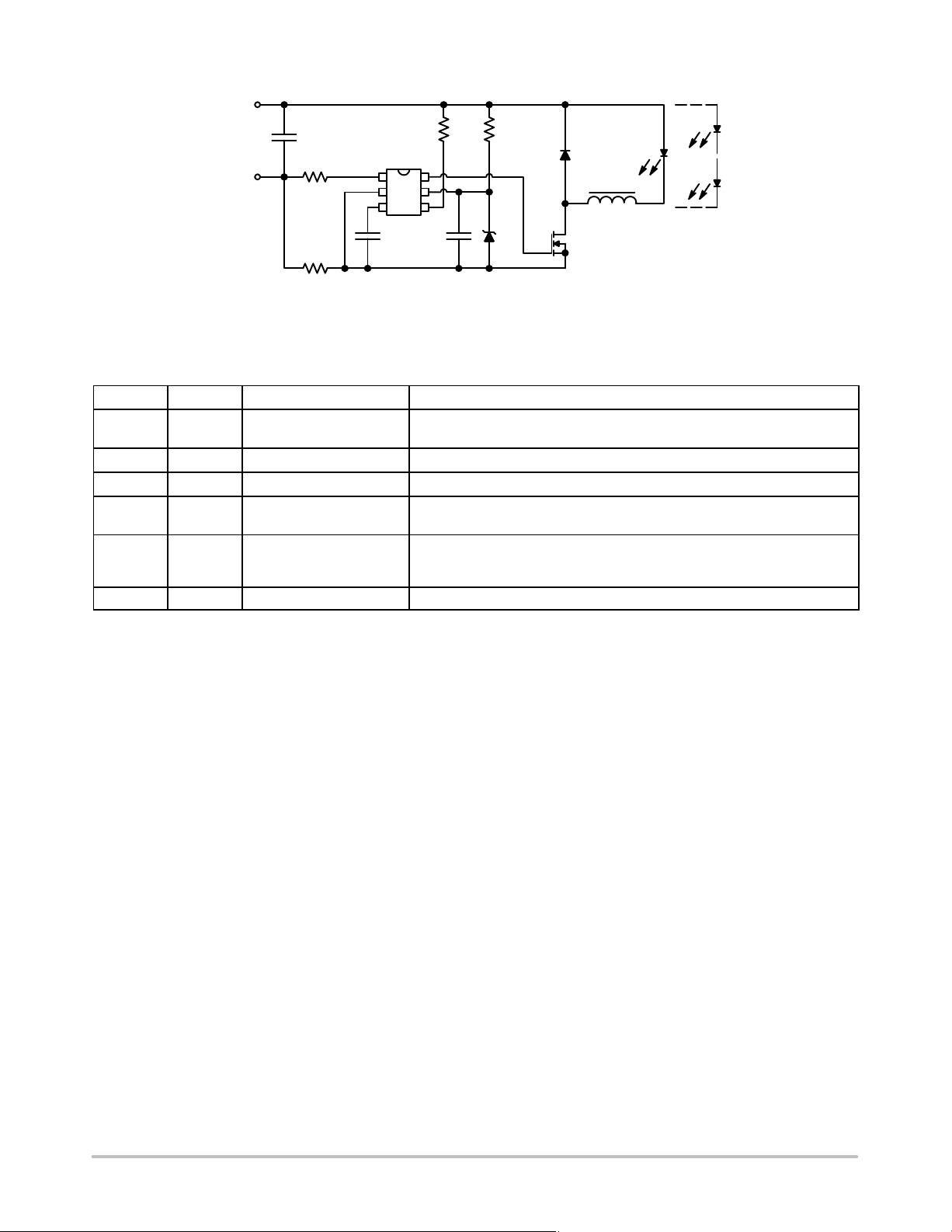
Figure 1. Typical Application Example of the LED Converter
PIN FUNCTION DESCRIPTION
Pin N5 Pin Name Function Pin Description
1 CS Current sense input A resistor divider consisting of R3 and R4 is used to set the peak current
2 GND Ground Power ground.
3 C
T
Timing capacitor Capacitor to establish the off time duration
4 IVC Input voltage compensation The current injected into the input varies the switch off time and I
5 V
CC
Input supply Supply input for the controller. The input is rated to 18 V but as illustrated
6 DRV Driver output Output drive for an external power MOSFET
sensed through the MOSFET switch
feedforward compensation.
Figure 1, a simple zener diode and resistor can allow the LED string to be
powered from a higher voltage
allowing for
PK
http://onsemi.com
2
Page 3
IVC
Input Voltage
Regulator
NCL30100
VDD
Reference
Iref
Regulator
Undervoltage
Lockout
V
CC
CT
CS
GND
50 mA
12.5−50 mA
Current Sense
Comparator
VOffset
0−3.9 V
OFF Time
Comparator
Reset
Set
S
R
SET
CLR
6.35/5.85 V
Gate Driver
Q
Q
DRV
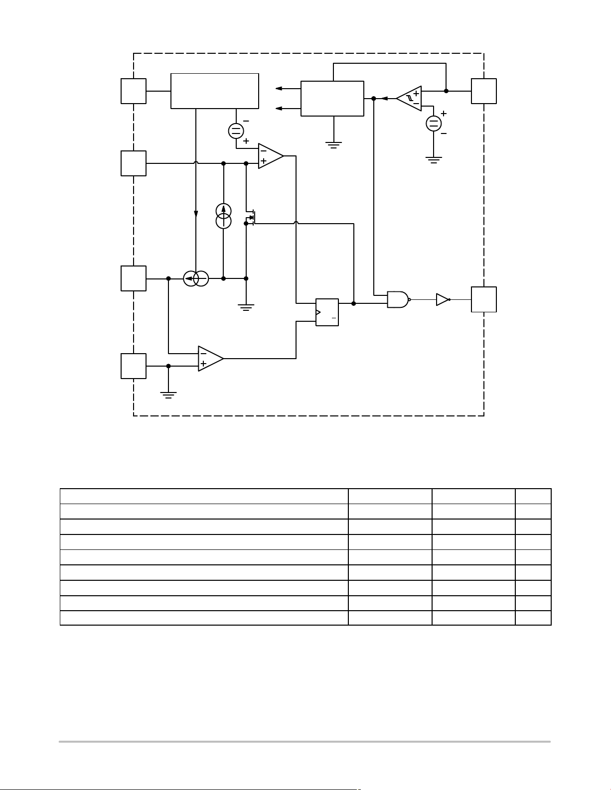
Figure 2. Simplified Circuit Architecture
MAXIMUM RATINGS
Rating Symbol Value Unit
Power Supply Voltage V
CC
IVC Pins Voltage Range IVC −0.3 to 18 V
CS and CT Pin Voltage Range V
Thermal Resistance, Junction−to−Air
Junction Temperature T
Storage Temperature Range T
ESD Voltage Protection, Human Body Model (HBM) V
ESD Voltage Protection, Machine Model (MM) V
in
R
q
JA
J
stg
ESD−HBM
ESD−MM
Stresses exceeding Maximum Ratings may damage the device. Maximum Ratings are stress ratings only. Functional operation above the
Recommended Operating Conditions is not implied. Extended exposure to stresses above the Recommended Operating Conditions may affect
device reliability.
1. This device(s) contains ESD protection and exceeds the following tests:
Human Body Model 2000 V per JEDEC Standard JESD22−A114E
Machine Model 200 V per JEDEC Standard JESD22−A115−A
2. This device meets latchup tests defined by JEDEC Standard JESD78.
3. Moisture Sensitivity Level (MSL) 1.
18 V
−0.3 to 10 V
178 °C/W
150 °C
−60 to +150 °C
2 kV
200 V
http://onsemi.com
3
Page 4
NCL30100
ELECTRICAL CHARACTERISTICS (V
= 12 V, for typical values TJ = 25°C, for min/max values TJ = −40°C to +125°C, unless
CC
otherwise noted)
SUPPLY SECTION
Parameter Conditions Symbol Min Typ Max Unit
INPUT VOLTAGE COMPENSATION
Offset Voltage
CT Pin Voltage
CT Pin Voltage
IVC pin internal resistance (Note 4) R
CT PIN – OFF TIME CONTROL
Source Current
Source Current CT Pin Grounded, −40 v T
Source Current Maximum Voltage Capability (Note 4)
Minimum CT Pin Voltage (Note 4) Pin Unloaded, Discharge Switch TurnedonV
Pin to ground capacitance (Note 4) C
Propagation Delay (Note 4) CT Reach VCT Threshold to Gate Output CT
CURRENT SENSE
Minimum Source Current
Minimum Source Current
Maximum Source Current
Maximum Source Current
Comparator Threshold Voltage (Note 4) V
Propagation Delay CS Falling Edge to Gate Output CS
GATE DRIVER
Sink Resistance
Source Resistance I
POWER SUPPLY
Startup Threshold
Minimum Operating Voltage VCC decreasing V
Vcc Hysteresis (Note 4) V
Startup Current Consumption VCC = 6 V I
Steady State Current Consumption
(Note 4)
Steady State Current Consumption C
4. Guaranteed by design
IVC Current = 25 mA (Including V
IVC Current = 50 mA (Including V
CT Pin Grounded, 0 v T
J
J
IVC = 180 mA, CT Pin Grounded,
0 v T
v 85°C
J
IVC = 180 mA, CT Pin Grounded,
−40 v T
v 125°C
J
IVC = 0 mA, CT Pin Grounded,
0 v T
v 85°C
J
IVC = 0 mA, CT Pin Grounded,
−40 v T
v 125°C
J
I
= 30 mA R
sink
= 30 mA R
source
VCC increasing V
C
= 0 nF, fSW = 100 kHz, IVC = open,
DRV
= 1 nF, fSW = 100 kHz, IVC = open,
DRV
V
= 7 V
CC
V
= 7 V
CC
) V
(offset)
) V
(offset)
v 85°C I
v 125°C I
V
(offset)
CT−25
CT−50mA
IVC
CT
CT
V
CT(max)
CT(min)
CT
delay
I
CS(min)
I
CS(min)
I
CS(max)
I
CS(max)
delay
OL
OH
CC(on)
CC(off)
CC(hyst)
CC1
I
CC2
I
CC2
1.10 1.30 1.45 V
1.69 2.08 2.47 V
mA
2.12 2.6 3.05 V
47.25 50 52.75
45.25 50 52.75
− 4.3 − V
− − 20 mV
− 8 − pF
− 220 − ns
11. 75 12.5 13.25
11.35 12.5 13.25
47.25 50 52.75
45.25 50 52.75
th
− 38 − mV
− 215 310 ns
5 15 40
20 60 100
− 6.35 6.65 V
5.45 5.85 − V
− 0.5 − V
− 22 35
0.5 1 1.15 mA
17
300
kW
mA
mA
mA
mA
mA
mA
W
W
mA
mA
http://onsemi.com
4
Page 5
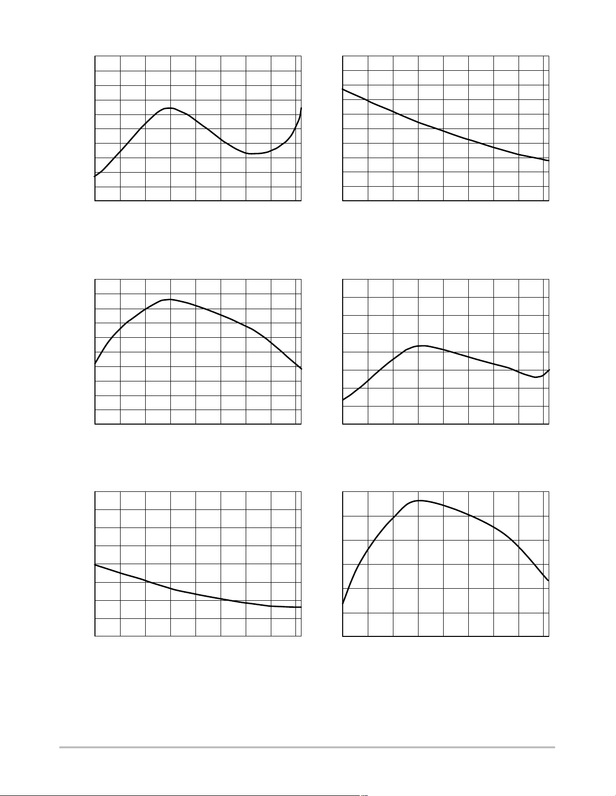
NCL30100
6.260
6.255
6.250
(V)
CC(on)
6.245
V
6.240
6.235
−40 −20 0 20 40 60 80 100 120
TEMPERATURE (°C)
Figure 3. V
Threshold vs. Junction
startup
Temperature
12.6
12.5
12.4
12.3
12.2
(mA)
12.1
12.0
CS(min)
I
11.9
11.8
11.7
11.6
−40 −20 0 20 40 60 80 100 120
TEMPERATURE (°C)
Figure 5. Minimum Source Current vs.
Junction Temperature
30
28
26
24
22
(mA)
20
CC1
I
18
16
14
12
10
−40 −20 0 20 40 60 80 100 120
TEMPERATURE (°C)
Figure 4. Startup Current Consumption vs.
Junction Temperature
5.780
5.775
5.770
5.765
(V)
5.760
CC(off)
5.755
V
5.750
5.745
5.740
−40 −20 0 20 40 60 80 100 120
TEMPERATURE (°C)
Figure 6. Minimum Operating Voltage
Threshold vs. Junction temperature
1.10
1.05
(mA)
1.00
CC2
I
0.95
0.90
−40 −20 0 20 40 60 80 100 120
TEMPERATURE (°C)
Figure 7. Steady State Current Consumption
vs. Junction Temperature
50.0
49.5
49.0
(mA)
48.5
CS(max)
I
48.0
47.5
47.0
http://onsemi.com
5
−40 −20 0 20 40 60 80 100 120
TEMPERATURE (°C)
Figure 8. Maximum Source Current vs.
Junction Temperature
Page 6
NCL30100
55
50
45
40
(mV)
th
V
35
30
25
−40 −20 0 20 40 60 80 100 120
TEMPERATURE (°C)
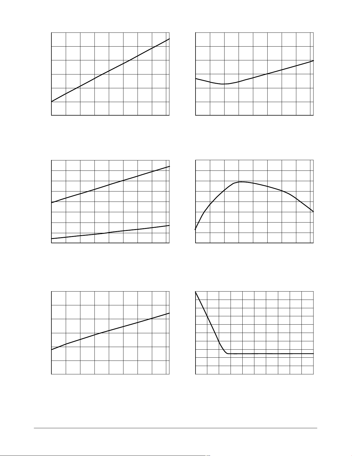
Figure 9. Comparator Threshold Voltage vs.
Junction Temperature
85
75
65
R
55
OH
1.350
1.345
1.340
(V)
1.335
(offset)
V
1.330
1.325
1.320
−40 −20 0 20 40 60 80 100 120
TEMPERATURE (°C)
Figure 10. Offset Voltage vs. Junction
Temperature
51.0
50.5
50.0
49.5
45
35
RESISTANCE (W)
25
R
15
5
−40 −20 0 20 40 60 80 100 120
OL
TEMPERATURE (°C)
Figure 11. Drive Sink and Source Resistance
vs. Junction Temperature
2.60
2.55
2.50
(V)
A
m
2.45
CT−50
V
2.40
2.35
2.30
−40 −20 0 20 40 60 80 100 120
TEMPERATURE (°C)
Figure 13. CT Pin Voltage vs. Input Voltage
Compensation Current
49.0
(mA)
CT
I
48.5
48.0
47.5
47.0
−40 −20 0 20 40 60 80 100 120
TEMPERATURE (°C)
Figure 12. CT Source Current vs. Junction
Temperature
50
45
40
35
30
25
(mA)
CS
I
20
15
10
5
0
0 20 20018016014012040 60 80 100
IVC (mA)
Figure 14. ICT Dependence on IVC Current
http://onsemi.com
6
Page 7
NCL30100
APPLICATION INFORMATION
The NCL30100 implements a peak current mode control
scheme with a quasi−fixed OFF time. An optional input
feedforward voltage control is provided to enhance
regulation response with widely varying input voltages.
Only a few external components are necessary to implement
the buck converter. The NCL30100 incorporates the
following features:
• Very Low Startup Current: The patented internal supply
block is specially designed to offer a very low current
consumption during startup.
• Negative Current Sensing: By sensing the total current,
this technique does not impact the MOSFET driving
voltage (V
) during switching. Furthermore, the
GS
programming resistor together with the pin capacitance
forms a residual noise filter which blanks spurious
spikes. This approach also supports a flexible resistor
selection. Finally unlike a positive sensing approach,
there is virtually no power dissipation in the current
sense resistor thus improving efficiency.
• Controller architecture supports high brightness LED
drive current requirements: Selection of the external
n−channel MOSFET can be easily optimized based on
operation voltage, drive current and size giving the
designer flexibility to easily make design tradeoffs.
• Typical $5.5% Current Regulation: The I
pin offers
CS
$5.5% from 0 to 85°C (+5.5% −9.5% across −40°C to
125°C) accuracy of the current typically, so the LED
peak current is precisely controlled
• No output capacitor is needed: By operating the
controller in continuous conduction mode, it is possible
to eliminate the bulky output filter capacitor.
The following section describes in detail each of the control
blocks
the switch and the inductor. This approach offers several
benefits over traditional positive current sensing.
• Maximum peak voltage across the current sense resistor
is user controlled and can be optimized by changing the
value of the shift resistor.
• The gate drive capability is improved because the
current sense resistor is located out of the gate driver
loop and does not deteriorate the switch on and also
switch off gate drive amplitude.
• Natural leading edge blanking is filter switching noise
at FET turn−in
• The CS pin is not exposed to negative voltage, which
could induce a parasitic substrate current within the IC
and distort the surrounding internal circuitry.
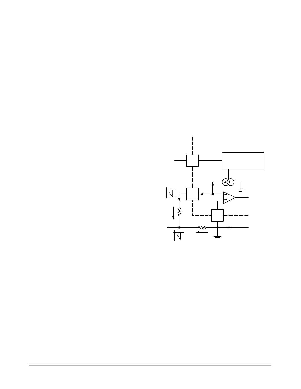
The current sensing circuit is shown in Figure 15.
IVC
Input Voltage
Regulator
12.5−50 mA
CS
To Latch
Vshift
Rshift
RCS
VCS
GND
Iprimary
Current Sensing Block
The NCL30100 utilizes a technique called negative
current sensing which is used to set the peak current through
http://onsemi.com
Figure 15. Primary Current Sensing
7
Page 8
NCL30100
Once the external MOSFET is switched on, the inductor
current starts to flow through the sense resistor R
current creates a voltage drop V
on the resistor RCS, which
CS
CS
. The
is negative with respect to GND. Since the comparator
connected to CS pin requires a positive voltage, a voltage
V
is developed across the resistor R
shift
source which level−shifts the negative voltage V
by a current
shift
CS
. The
level−shift current is in the range from 12.5 to 50 mA
depending on the optional input voltage compensation loop
control block signal (see more details in the input voltage
compensation section). The peak inductor current is equal
to:
I
@ R
* V
Ipk+
R
shift
CS
To achieve the best Ipk precision, higher values of I
CS
th
(eq. 1)
CS
should be used. The Equation 1 shows the higher drop on
R
reduces the influence of the Vth tolerance. Vth is the
CS
comparator threshold which is nominally 38 mV.
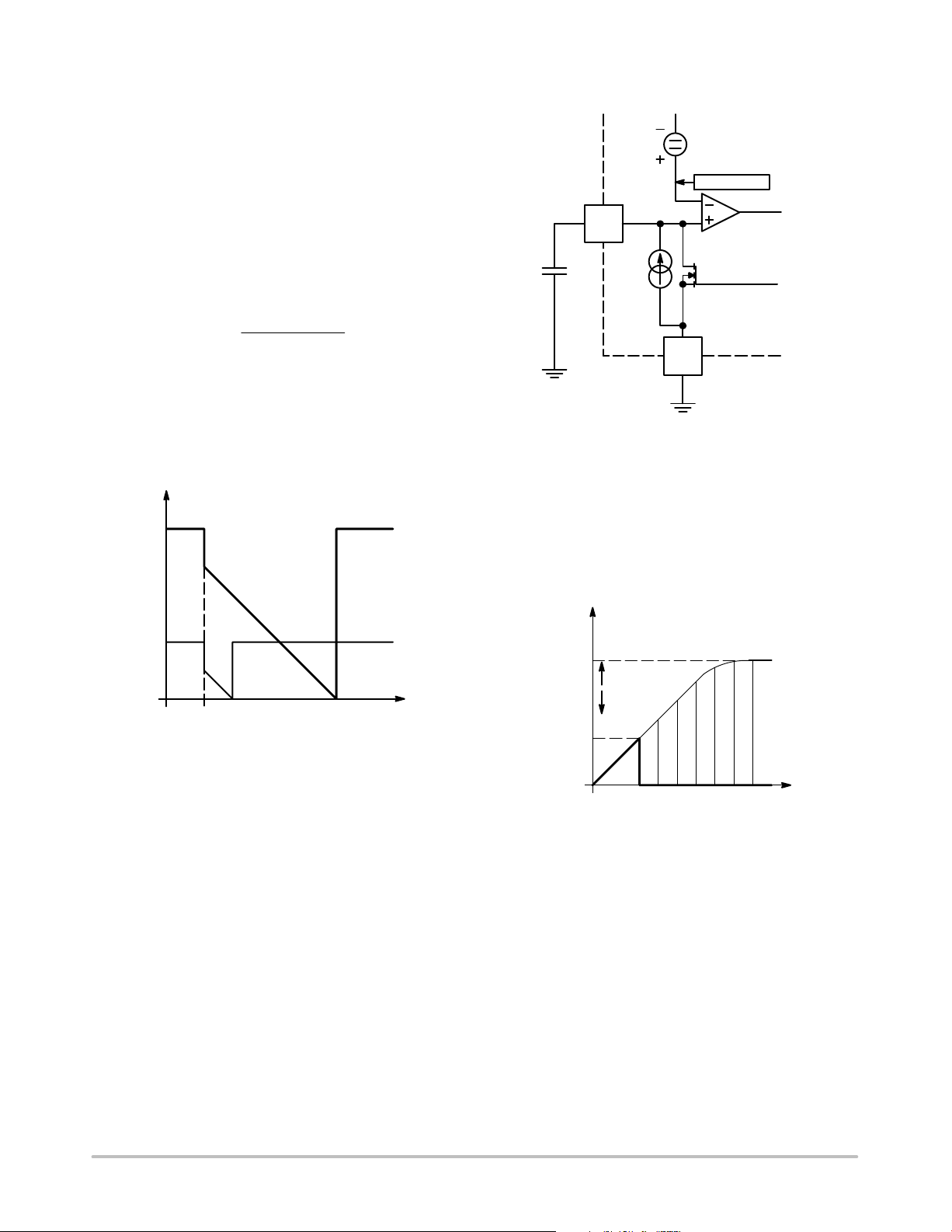
A typical CS pin voltage waveform for continuous
condition mode is shown in Figure 16.
V
I
shift = 50 mA
From Input Voltage
Compensation Block
VOffset
VOffset to VDD
CT
CT
50 mA
To Latch’s Set Input
To Latch’s Output
GND
Figure 17. OFF Time Control
During the switch−on time, the CT capacitor is kept
discharged by an internal switch. As soon as the latch output
changes to a low state, the I
across C
threshold given by the V
starts to ramp−up until its value reaches the
T
offset
is enabled and the voltage
source
. The current injected into IVC
can change this threshold. The IVC operation will be
discussed in the next section.
shift = 12.5 mA
I
0
Switch
Turn on
t
Figure 16. CS Pin Voltage
Figure 16 also shows the effect of the inductor current
based on the range of control possible via the IVC input.
OFF Time Control
The internal current source, together with an external
capacitor, controls the switch−off time. In addition, the
optional IVC control signal can modulate the off time based
on input line voltage conditions. This block is illustrated in
Figure 17.
V
VDD
Goes Up
I
CT pin
Voltage
Voffset
VC
Goes Down
I
VC
I3
I2
t
off−min
I1
t
0
Figure 18. CT Pin Voltage
The voltage that can be observed on CT pin is shown in
Figure 18. The bold line shows the minimum IVC current
when the off time is at its minimum. The amount of current
injected into the IVC input can increase the off time by
changing the turn off comparator switching threshold. I1, I2,
http://onsemi.com
8
Page 9
NCL30100
and I3 represent different delays depending on the
magnitude of IVC.
V
CC
Gate Driver
The Gate Driver consists of a CMOS buffer designed to
directly drive a power MOSFET. It features unbalanced
source and sink capabilities to optimize switch on and off
performance without additional external components. The
power MOSFET is switched off at high drain current, to
minimize its switch off losses the sink capability of the gate
driver is increased for a faster switch off. On the other hand,
the source capability of the driver is reduced to slow−down
the power MOSFET at switch on in order to reduce EMI
generation. Whenever the IC supply voltage is lower than
the under voltage threshold, the Gate Driver is low, pulling
down the gate to ground thus eliminating the need for an
external resistor.
Input Voltage Compensation:
The Input Voltage Compensation block gives the user
optional flexibility to sense the input voltage and modify the
current sense threshold and off time. This function provides
a feed forward mechanism that can be used when the input
voltage of the controller is loosely regulated to improve
output current regulation. If the input voltage is well
regulated, the IVC input can also be used to adjust the offset
of the off time comparator and the current sense control to
achieve the best current regulation accuracy.
An external resistor connected between IVC and the input
supply results in a current being injected into this pin which
has an internal 17 kW resistor connected to a current mirror.
This current information is used to modify V
By changing V
the off time comparator threshold is
offset
offset
and ICS.
modified and the off time is increased. A small capacitor
should be connected between the IVC pin and ground to
filter out noise generated during switching period. Figure 19
shows the simplified internal schematic:
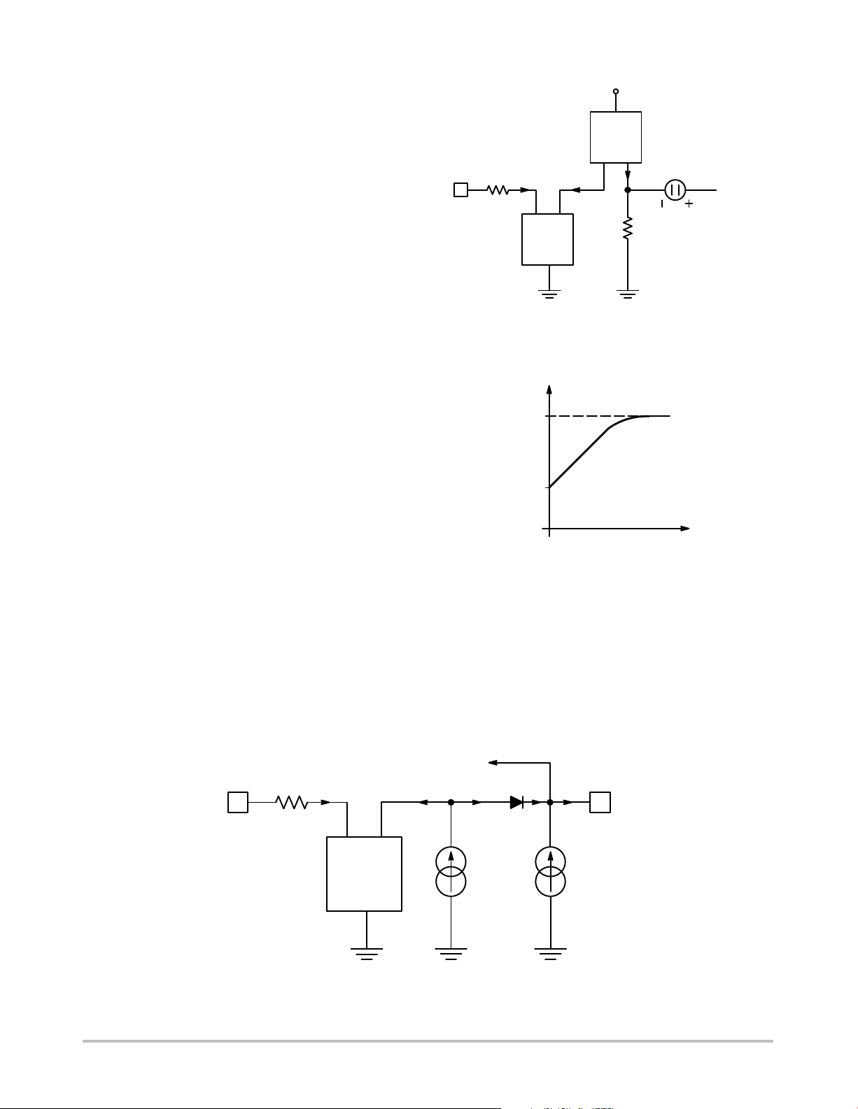
Current
Mirror
1:1
25 kW
VOffset
To OFF
Time
Comparator
mA
17 kW
IVC
Current
Mirror
1:1
Figure 19. Input Voltage Compensation, OFF Time
Control
V
VDD
Voltage
Voffset
OFF Time Comparator Input
0
IVC Pin Sink Current
Figure 20. IVC Loop Transfer Characteristic
The transfer characteristic (output voltage to input
current) of the input voltage compensation loop control
block can be seen in Figure 20. V
refers to the internal
DD
stabilized supply. If no IVC current is injected, the off time
comparator is set to V
offset
.
The value of the current injected into IVC also change Ics.
This is accomplished by changing the voltage drop on R
shift
The corresponding block diagram of the IVC pin can be seen
in Figure 21.
.
To Current Sense Comparator
17 kW
IVC
Current
Mirror
4:3
Figure 21. Input Voltage Compensation Loop – Current Sense Control
http://onsemi.com
9
37.5 mA
CS
12.5 mA
Page 10
NCL30100
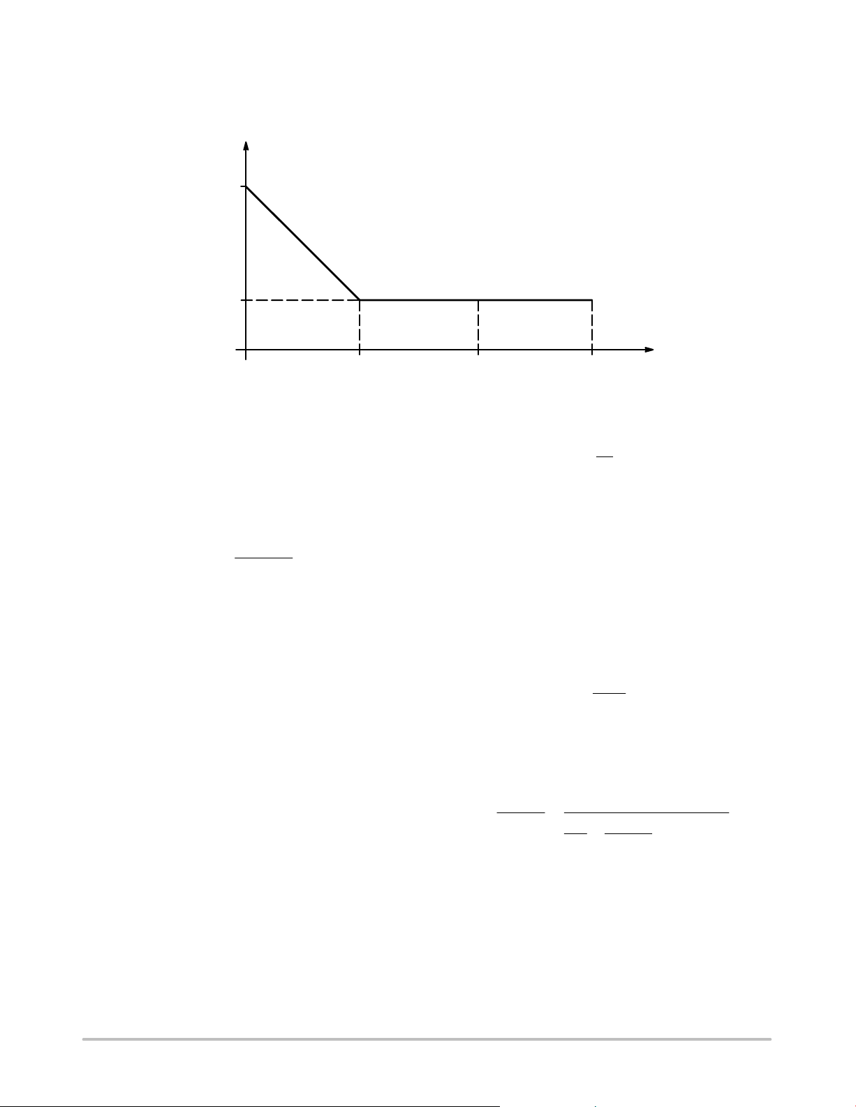
The current sense characteristic can be seen in Figure 22.
As illustrated, by varied the IVC current between 0 − 50 mA,
the sourcing current can range from 12.5 to 50 mA.
V
50 mA
12.5 mA
CS Pin Source Current
0 mA
50 mA
IVC Pin Sink Current
Figure 22. Current Sense Regulation Characteristic
Biasing the controller
The NCL30010 Vcc input can range up to 18 V. For
applications that have an input voltage that is greater than
that level, an external resistor should be connected between
V
and the VCC supply capacitor. The value of the resistor
in
can be calculated as follows:
V
* V
in
R2+
I
CC
CC2
(eq. 2)
Where:
V
− Voltage at which IC operates (see spec.)
CC
I
– Current at steady state operation
CC2
V
− Input voltage
in
The I
current is composed of two components: The
CC
quiescent current consumption (300 mA) and the switching
current consumption. The driver consumption depends on
the MOSFET selected and the switching frequency. Total
current consumption can be calculated using following
formula:
ICC+ 300 @ 10−6) C
MOSFET
@ VCC@ f
switching
(eq. 3)
In applications where the input voltage Vin is varying
dramatically, a zener can be used to limit the voltage going
into V
Switching Frequency
, thus reducing the switching current contribution.
CC
The switching frequency varies with the output load and
input voltage. The highest frequency appears at highest
input voltage. Since the peak inductor current is fixed, the
on−time portion of the switching period can be calculated:
I
V
pk
in
mA
) CS
delay
(eq. 4)
100 mA 140 mA
ton+ L @
Where:
L − Inductor inductance
I
− Peak current
pk
As seen from the above equation, the turn on time depends
on the input voltage. In the case of a low voltage AC input
where there is ripple due to the time varying input voltage
and input rectifier, natural frequency dithering is produced
to improve the EMI signature of the LED driver.
The turn off time is determined by the charging of the
external capacitor connected to the CT pin. The minimum
t
value can be computed as:
off
V
t
off
+ CT@
offset
I
CT
) CT
delay
(eq. 5)
Where:
V
− Offset voltage (see parametric table)
offset
I
− CT pin source current (see parametric table)
CT
Finally, the switching frequency then can be evaluated by:
FSW+
1
+
t
) t
on
L@I
off
pk
)
V
in
The sum of the nominal CS
CT@V
50@10
1
offset
−6
delay
) 435 @ 10
and CT
−9
(eq. 6)
delay
is
approximately 435 nsec.
http://onsemi.com
10
Page 11
NCL30100
Reverse Buck Operating Description
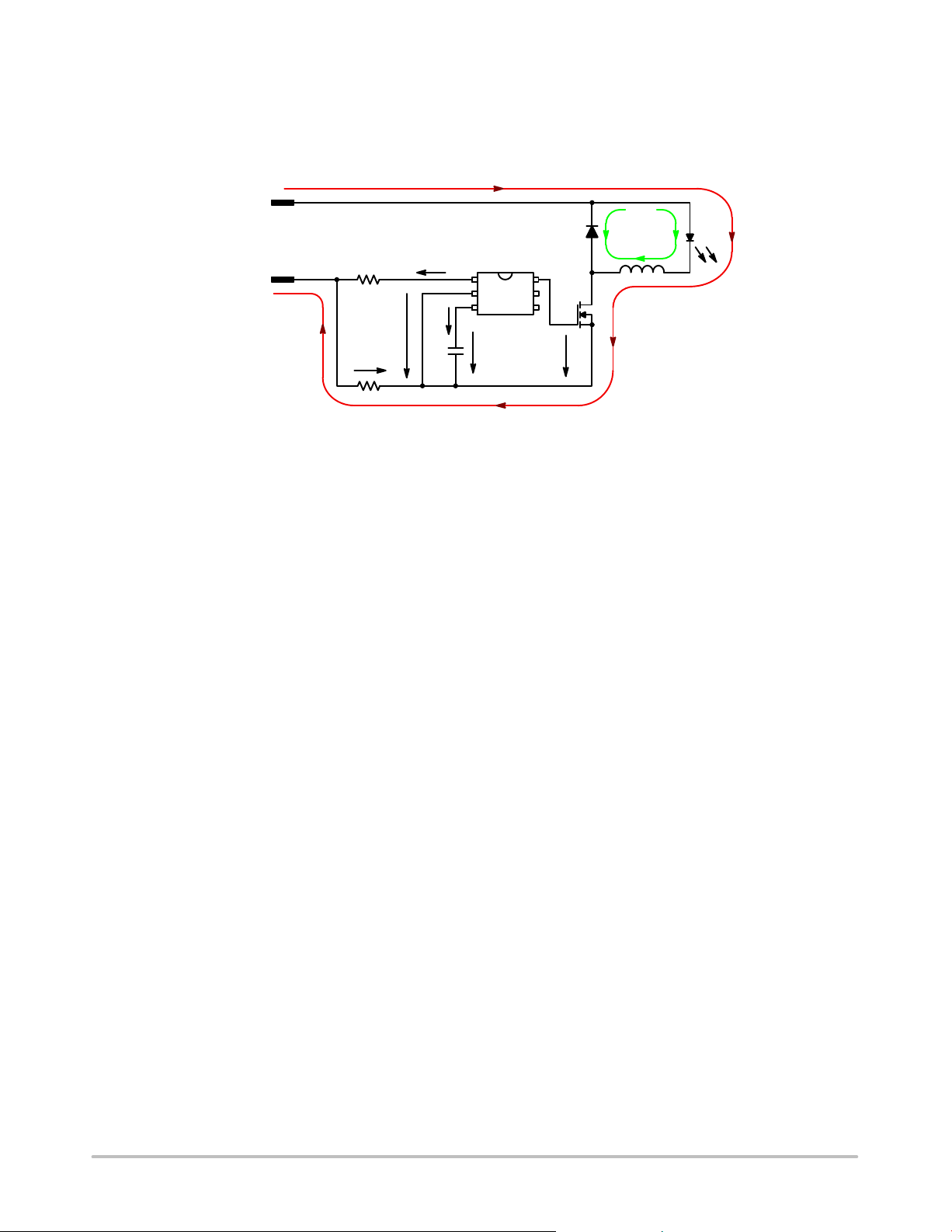
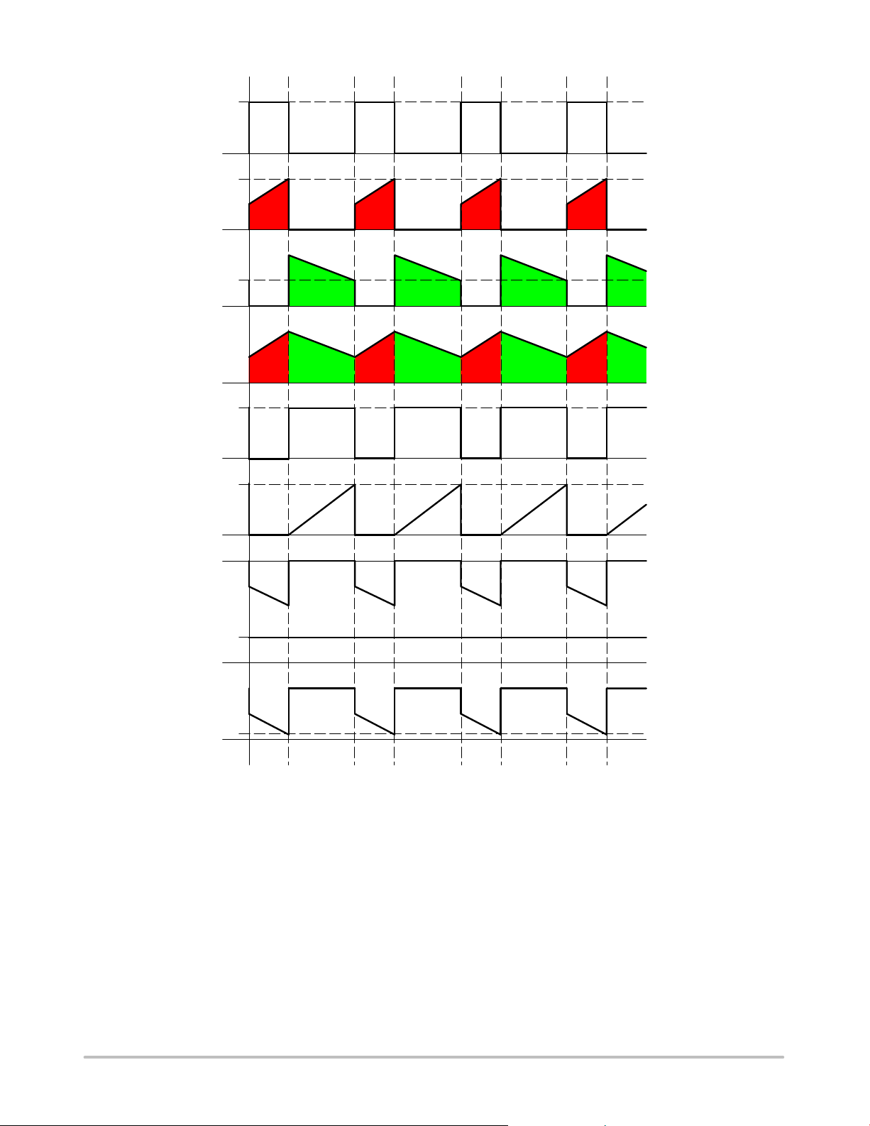
Figure 23 illustrates a typical application schematic and
Figure 24 displays simplified waveforms illustrate the
converter in steady state operation for critical circuit nodes.
Imag
Vin
D1
1
2
GND
3
VCT
IC1
NCL30100
CS
CT
DRV
VCC
IVC
6
5
4
VDRV
Q1
Rshift
Vsense
Rsense
ICS
ICT
VCS
CT
Figure 23. Simplified Application Schematic
Idemag
L1
LED
http://onsemi.com
11
Page 12
Vcc
V
I
50 uA
DRV
Ipk
I
mag
demag
Imin
I
LED
I
NCL30100
0
0
0
0
CT
0
V
CT
0
0
V
Sense
I
CS
0
V
CS
38 mV
0
Figure 24. Voltage and Current Nodes in the Application Circuit
The current follows the red line in Figure 23 when Q1 is
turned on. The converter operates in continuous conduction
mode therefore the current through the inductor never goes
to zero. When the switch is on, the current creates a negative
voltage drop on the R
not be measured directly by the IC so an R
resistor. This negative voltage can
sense
resistor is
shift
connected to CS pin. Inside the IC there is a current source
connected to this pin. This current source creates constant
voltage drop on resistor R
voltage drop presented on R
current I
R
sense
increases linearly, the negative voltage on
mag
increased as well. Thus the voltage on CS pin
which shifts the negative
sense
positive. The magnetizing
sense
approaching zero. On the CS pin there is a comparator with
a reference level of 38 mV. Once the voltage on the CS pin
reaches this reference level, the DRV output is turned off and
current path I
disappears. Energy stored in the inductor
mag
as a magnetic field keeps current flowing in the same
direction. The current path is now closed via diode D1
(green line). Once the DRV is turned off, the internal current
source starts to charge the CT capacitor and the voltage on
this node increases. Once the CT capacitor voltage reaches
the V
level, Q1 is turned on and an internal switch
CT
discharges the CT capacitor to be ready for the next
switching cycle.
http://onsemi.com
12
Page 13
NCL30100
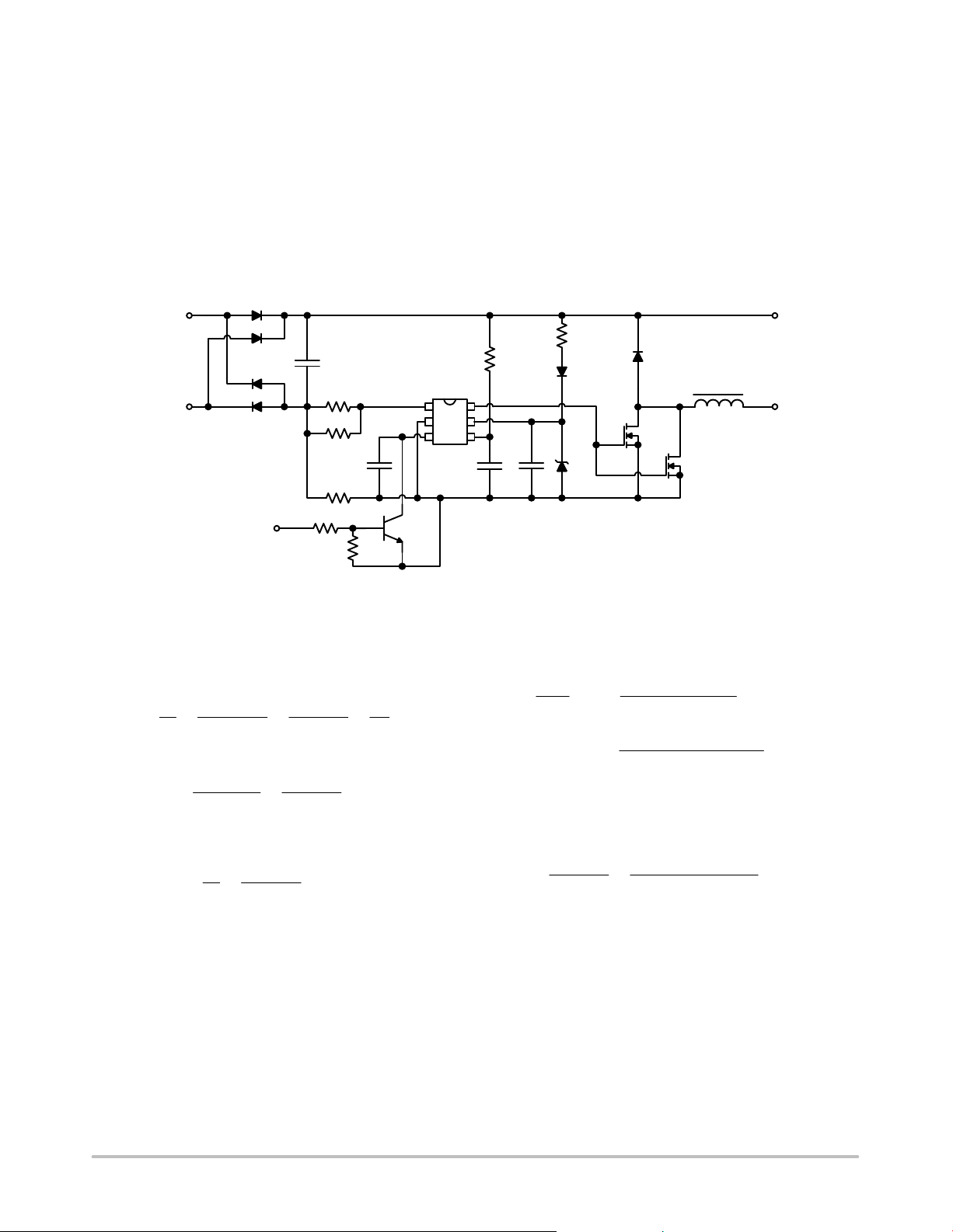
Application Design Example:
A typical step down application will be used to illustrate the basic design process based on nominal design parameters:
• Input voltage: V
− 12 Vac (12 V dc after the bridge)
in
• Nominal LED current: 700 mA (rms)
• LED
• V
LED
• Freewheel diode V
: 120 mA (peak−to−peak)
ripple
: 3.2 V
: 0.5 V
f
• Target Switching Frequency: 450 kHz
Dimming using PWM signal 1 kHz with duty cycle 0 – 99%
Vac
Vac
DIMM
0/5 V
12 V
D4
D5
D6
D7
C1
R3
R5
C2
R4
R9
R8
NCL30100
IC1
CS
GND
CT
Figure 25. Example Design Schematic
Note this simplified step−by−step design process neglects
any parasitic contribution of the PCB.
First, we need to determine the nominal t
V
) V
LED
f
+
3.2 ) 0.5
12 * 3.2
on
off
+
Vin* V
LED
t
t
ON/tOFF
+
3.7
8.8
ratio:
(eq. 7)
Next the typical duty cycle (DC) will be calculated:
DC +
ON
tON) t
OFF
+
3.7 ) 8.8
3.7
+ 0.296
(eq. 8)
t
Target switching frequency is set at 450 kHz, now we need
to determine the period:
1
T +
f
op
Combination the previous equation we can calculate the t
and t
durations:
OFF
tON+ DC @ T + 0.296 @ 2.222 @ 10−6+ 658 ns
t
+(1 * DC)@ T +(1 * 0.296)@ 2.222 @ 10
OFF
+ 1.564 ms
+
450 @ 10
1
+ 2.222 ms
3
(eq. 9)
ON
(eq. 10)
−6
R2
D1
L3
Q1
Q2
DRV
VCC
R1
D3
IVC
C3
C5
D2
Now all the parameters are defined to calculate inductor
value:
V +
di @ L
dt
å L +
+
ǒ
VIN* V
(
12 * 3.2)@ 658 @ 10
I
ripple
LED
0.12
Ǔ
@ t
ON
−9
A standard value 47 mH is chosen.
Next the CT capacitor can be calculated, but we need to
first determine the IVC current which can be simply
calculated.
I
IVC
+
V
R ) R
IVC
+
1.5 @ 10
12
6
) 17 @ 10
3
The IVC current controls the dependence of the peak
current to the input voltage. If the input voltage is well
regulated, the IVC pin should be grounded. The value for
IVC resistor should be chosen based on graphs below.
Note as well that the IVC can be used to implement analog
dimming since increasing the current into IVC pin will
decrease the I
of the LED).
peak
A
K
(eq. 11)
^ 48.3 mH
^ 7.91 mA
(eq. 12)
http://onsemi.com
13
Page 14
NCL30100
1000
900
800
700
600
(mA)
500
LED
I
400
300
200
100
7 8 9 101112131415161718
Rivc = 300k
Rivc = 510k
Rivc = 1 Meg
Rivc = 1.5 Meg
Rivc = 2.2 Meg
Rivc = 3.7 Meg
Rivc = infinity
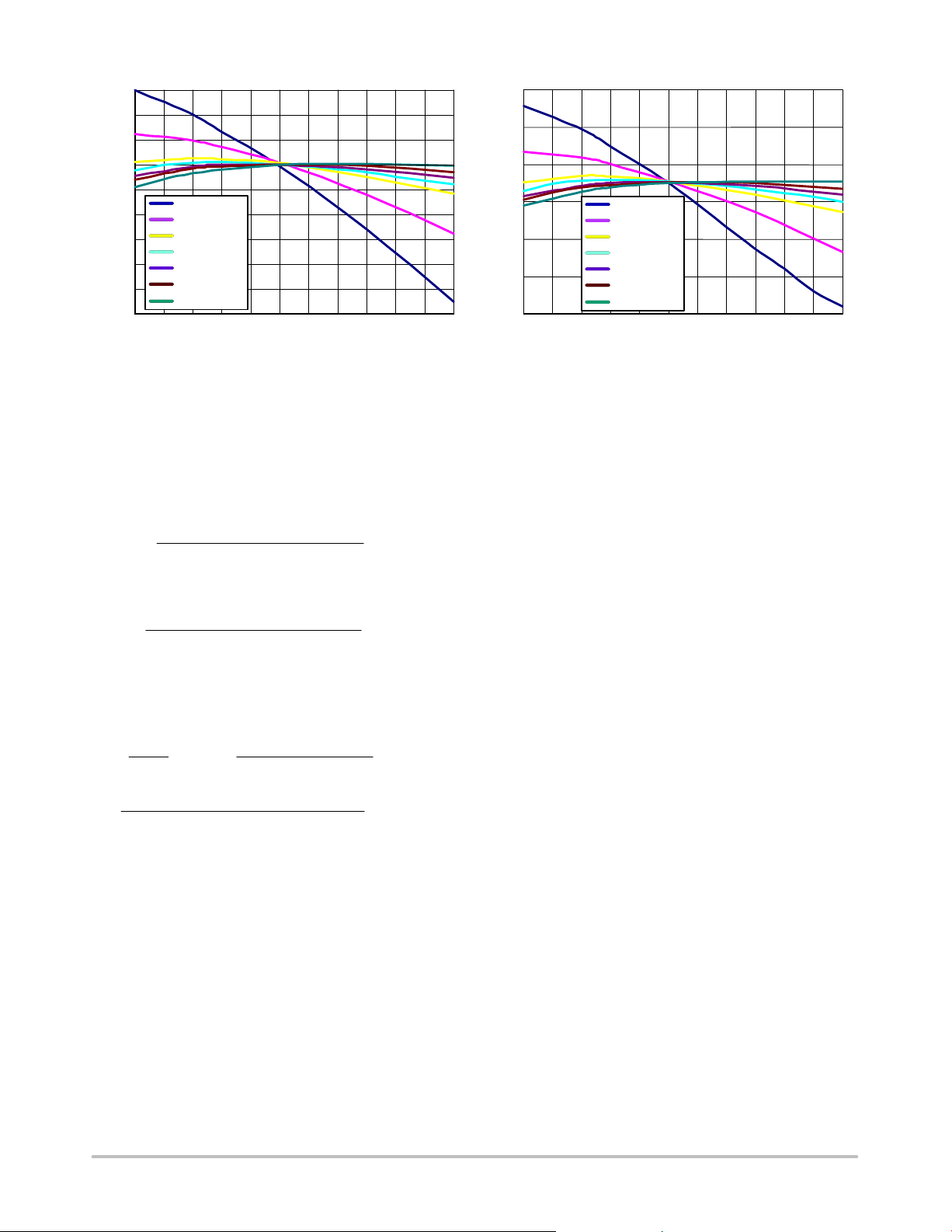
Figure 26. R
INPUT VOLTAGE (V)
Impact versus Vin for I
ivc
LED
=
700 mA Nominal
A value 1.5 MW was used since the input voltage has a
sinusoidal component due to the low voltage AC input and
desires to have a small bulk capacitance, thus compensating
for part of this variation.
The dependence of V
on IVC current is described by the
CT
following equation:
2
VCT+
−0.097 @ X
) 24.5 @ X ) 1358.1
976.8
[V]
(eq. 13)
Using the result from Equation 12 and put it to Equation 13
the V
threshold will be calculated:
CT
2
VCT+
−0.097 @ 7.91
^ 1.58 V
) 24.5 @ 7.91 ) 1358.1
976.8
(eq. 14)
The CT capacitance can be calculated using the equations
above:
I +
50 @ 10
+
dv @ C
dt
@ǒt
OFF
V
CT
* CT
I
å CCT+
−6
@ǒ1.654 @ 10−6* 220 @ 10
CT
1.58
delay
−9
Ǔ
Ǔ
(eq. 15)
^ 45.8 pF
The intrinsic pin capacitance CT pin (~8 pF) in
conjunction with the dimming transistor (~10 pF) in this
schematic approximately 18 pF so this value must be
subtracted from the calculated value in Equation 15. The
600
500
400
300
(mA)
LED
I
200
100
0
7 8 9 10 11 12 13 14 15 16 17 18
Figure 27. Rivc Impact versus Vin for I
Rivc = 300k
Rivc = 510k
Rivc = 1 Meg
Rivc = 1.5 Meg
Rivc = 2.2 Meg
Rivc = 3.7 Meg
Rivc = infinity
INPUT VOLTAGE (V)
LED
=
350 mA Nominal
calculated value is not standard, so the nearest value 33 pF
has been selected.
Now we can calculate the I
of LED. The average value
PK
is set to 700 mA and the target ripple is set at 120 mA, the
I
equals 760 mA. R
PK
has been chosen to be as small a
shift
voltage drop as possible to minimize power dissipation so an
of 100 mW has been selected.
R
shift
Before calculation of R
current, which affects the offset on R
we need to know the I
shift
. The ICS value
shift
dependents on the IVC current and for IVC currents between
0 − 50 mA, it can be described by this formula:
ICS+ −0.75 @ IVC ) 50 @ 10
[mA]
(eq. 16)
−6
Therefore:
ICS+ −0.75 @ IVC ) 50 @ 10
+ −0.75 @ 7.91 @ 10−6) 50 @ 10−6^ 44.07 mA
To calculate R
it is necessary to know the Ipk current
shift
−6
(eq. 17)
through the inductor. From the time that the current sense
comparator detects that the peak current threshold has been
crossed to the time that the external MOSFET switch is
turned off there is a propagation delay. Depending on the
value of the inductor selected (which is based on the target
switching frequency), there is a current error between the
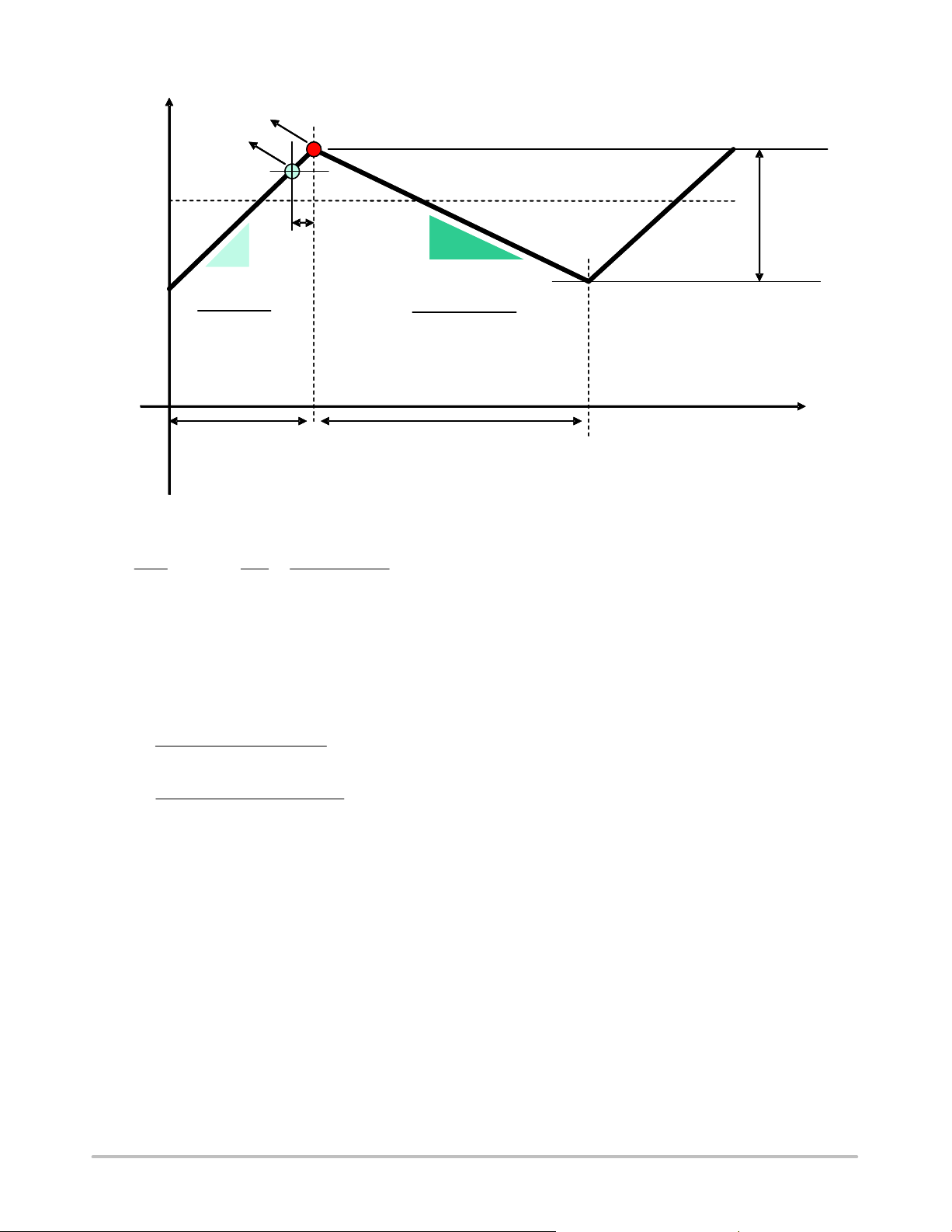
intended peak current and the actual peak current, this is
illustrated in Figure 28.
CS
http://onsemi.com
14
Page 15
I
I
LED
LED
I
I
peak
peak
I
I
cs
cs
NCL30100
Δi
L
t
t
d
d
(Vin-V
(Vin-V
Figure 28. A Current Error Between the Intended Peak Current and the Actual Peak Current
di @ L
V +
^ 0.0402 A
V/L is simply the slew rate through the inductor and td is
the internal propagation delay so the current overshoot from
target is approximately 40 mA as calculated in Equation 18.
All values necessary for R
R
value is described by this formula:
shift
R
shift
This value of resistance can be a parallel combination of
2.7 kW and 30 kW.
To understand the operating junction temperature, we
calculate the die power dissipation:
P
DIE
å I
dt
R
sense
+
0.1 @(0.76 * 0.0402)) 0.038
+
+ VCC@ǒ300 @ 10−6) C
+ 12 @ǒ300 @ 10−6) 560 @ 10
+ 39.8 mW
+
delay
@ǒIpk* I
44.07 @ 10
L
L
I
CS
LED
LED
t
t
on
on
V @ t
)
)
8.8 @ 215 @ 10
+
L
delay
47 @ 10
calculation are known, the
shift
Ǔ
) V
−6
MOSFET
−6
th
^ 2496 W
@ VCC@ f
−12
@ 12 @ 450 @ 10
−9
-V
-V
-V
(eq. 18)
(eq. 19)
switching
(eq. 20)
LED
LED
LED
t
t
Ǔ
3
off
off
Ǔ
- V
- V
- V
diode
diode
diode
L
L
L
Using the P
TempIC+ TA) P
A design spreadsheet to aid in calculating the external
components necessary for a specific set of operating
conditions is available for download at the
ON Semiconductor website.
For a low voltage AC input diode D3 is placed into the Vcc
line. Since Capacitor C3 is charged from a sinusoidal
voltage. If the input voltage approaches zero, the IC is still
supplied from C3. Due to this diode, the IC keeps the LED
driver operating even if the sinusoidal voltage is lower than
V
CC(min)
make sense only if a single LED is used and the converter is
supplied by sinusoidal voltage 12 Vac. For two LEDs in
series their forward voltage is almost as high as V
the IC.
Parasitic capacitance and inductance are presented in real
applications which will have an influence on the circuit
operation. They are depending on the PCB design which is
user dependent. The BOM, PCB and some plots are enclosed
for better understanding of the system behavior.
, we can calculate junction temperature:
DIE
@ R
DIE
+ TA) 7.1° C
until Vin is lower than V
+ TA) 0.0399 @ 178
qJA
. The use of this diode
LED
(eq. 21)
CC(min)
of
http://onsemi.com
15
Page 16
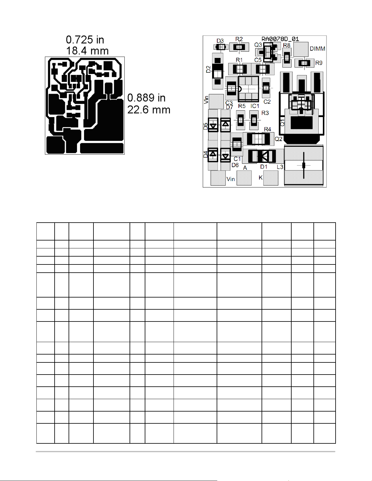
Figure 29. PCB Design the Circuit Calculated Above.
Only Single Layer PCB is Used for the Application.
NCL30100
Figure 30. The Component Side (Several Transistor
Packages are Possible to Use)
BILL OF MATERIALS FOR THE SINGLE LAYER EVALUATION BOARD (NCL30100ASLDGEVB)
Des-
ignat-
or
C1 1 Capacitor
C2 1 Capacitor 33 pF 5% 0603 Kemet C0603C330J5GACTU Yes Yes
C3 1 Capacitor
C5 1 Capacitor 1 nF 10% 0603 Kemet C0603C104K5RACTU Yes Yes
D1 1 Surface
D2 1 Zener
D3 1 Schottky
D4,
D5,
D6,
D7
IC1 1 LED
L3 1 Inductors
Q1 1 Power
Q2 1 Power
Q2 1 Power
Q2 1 Power
Q2 1 Power
Q3 1 General
Descrip-
Qty
tion
Mount
Schottky
Power
Rectifier
Diode
Diode
4 Schottky
Diode
Driver
MOSFET
MOSFET
MOSFET
MOSFET
MOSFET
Purpose
Transistor
NPN
Manufacturer
Value Tol Footprint Manufacturer
2.2 mF / 25 V
4.7 mF / 25 V
MBR130T3G − SOD−123 ON Semiconductor MBR130T3G No Yes
16 V 5% SOD−123 ON semiconductors MMSZ16T1G No Yes
NSR0520V2T1G − SOD−523 ON semiconductors NSR0520V2T1G No Yes
NSR0340HT1G − SOD−323 ON semiconductors NSR0340HT1G No Yes
NCL30100 − TSOP−6 ON semiconductors NCL30100SNT1G No Ye s
47 mH
NTGS4141NT1G − TSOP−6 ON semiconductors NTGS4141NT1G No Ye s
NU − SOT−223 ON semiconductors NTF3055−100T1G No Ye s Option
NU − DPAK ON semiconductors NTD23N03RT4G No Ye s Option
NU − SOT−363 ON semiconductors NTJS4160NT1G No Yes Option
NU − SOT−23 ON semiconductors NTR4170NT1G No Ye s Option
BC817−16 − SOT−23 ON semiconductors BC817−16LT1G No Ye s
10% 0805 AVX 08053C225KAT2A Ye s Yes
10% 0805 AVX 08053D475KAT2A Ye s Yes
10% WE−PD2_M Wurth Electronik 744774147 No Ye s
Part Number
Substitution
Allowed
Pb−Free
Com-
ments
http://onsemi.com
16
Page 17
NCL30100
BILL OF MATERIALS FOR THE SINGLE LAYER EVALUATION BOARD (NCL30100ASLDGEVB)
Des-
ignat-
or
Q3 1 Power
R1 1 Resistor 1.5 M 1% 0603 Rohm Semiconductor MCR03EZPFX1504 Ye s Yes
R2 1 Resistor 300 R 1% 0603 Rohm Semiconductor MCR03EZPFX3000 Yes Ye s
R3 1 Resistor 30 k 1% 0603 Rohm Semiconductor MCR03EZPFX3002 Yes Yes
R4 1 Resistor 0.1 R 1% 0805 Welwyn LRCS0805−0R1FT5 Ye s Yes
R5 1 Resistor 2.7 k 1% 0603 Rohm Semiconductor MCR03EZPFX2701 Ye s Yes
R8 1 Resistor 10 k 1% 0603 Rohm Semiconductor MCR03EZPFX1002 Yes Yes
R9 1 Resistor 5.6 k 1% 0603 Rohm Semiconductor MCR03EZPFX5601 Ye s Yes
Qty
Descrip-
tion
MOSFET
ManufacturerFootprintTolValue
NU − SOT−23 ON semiconductors NTS4001NT1G No Yes Option
Manufacturer
Part Number
Substitution
Allowed
Pb−Free
Com-
ments
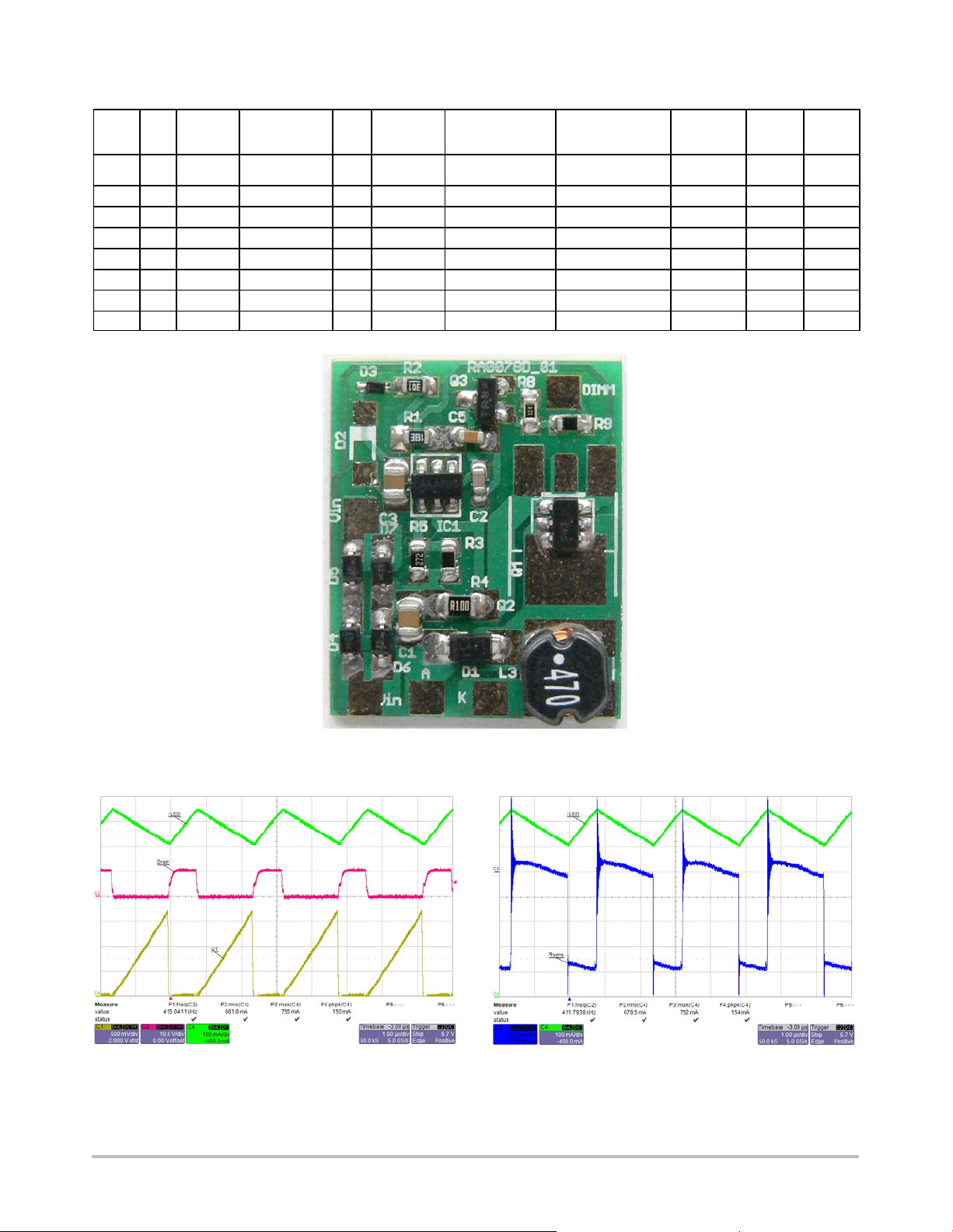
Figure 31. Completed PCB with Devices
Figure 32. Snapshot of CT Pin Voltage, Driver and
ILED
http://onsemi.com
Figure 33. Voltage Measured on RCS (R4)
17
Page 18
NCL30100
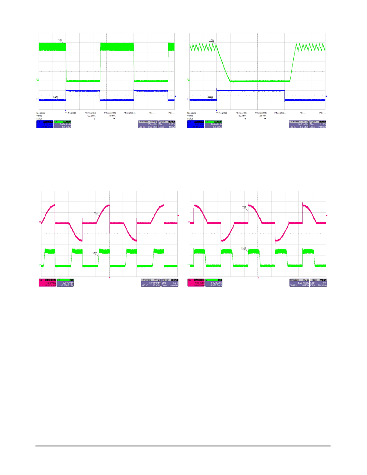
Figure 34. Current Through LED if 50% Dimming
at 1 kHz is Applied
Figures 36 and 37 illustrate leading edge and trailing edge
waveforms from a chopped AC source. For proper dimming
control, the bulk capacitance must be reduced to a relatively
small value to achieve best dimming range. Performance in
Figure 36. Trailing Edge Dimming Figure 37. Leading Edge (Triac) Regulation. Small
Figure 35. The Dimming Detail at 95%. No Overshoot
in LED Current is Observed
real world application is dependent on the characteristics of
the actual dimmer and the electronic transformer used to
generated to chopped AC waveform
Overshoot is Seen on the Leading Edge, this is
Based on the Abrupt Chopping of the Low Voltage
AC Waveform
http://onsemi.com
18
Page 19
NCL30100
6
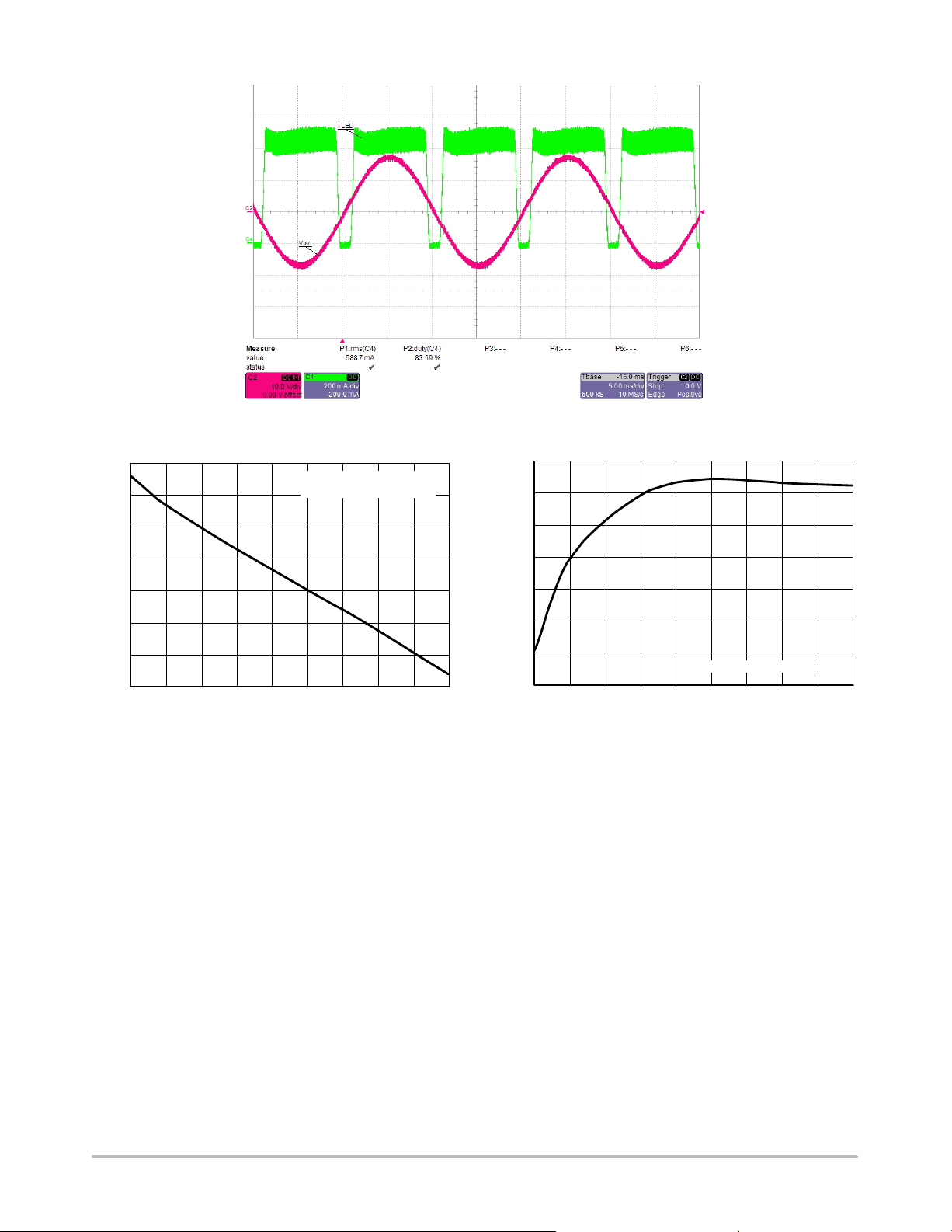
Figure 38. ILED and Vin Waveform if No Dimming is Used
84
83
82
81
80
EFFICIENCY (%)
79
78
77
7 8 9 10111213141516
INPUT VOLTAGE (V)
DC Voltage Efficiency
(No Bridge Rectifier)
Figure 39. Efficiency Measurement for the
Demoboard (V
= 3.2 Nominal)
f
Figure 39 represents the efficiency of the converter
driving a single LED at a nominal current of 690 mA. The
addition of the AC bridge rectifier contributes addition
losses into the circuit and it is recommended to us low
forward voltage schottky rectifiers to minimize power
dissipation in the AC rectification stage.
690
680
670
660
650
CURRENT (mA)
640
630
620
7 8 9 1011121314151
INPUT VOLTAGE (V)
Figure 40. I
Current Dependence on Input
LED
LED Current Variation
DC Voltage (No Bridge Rectifier is Used)
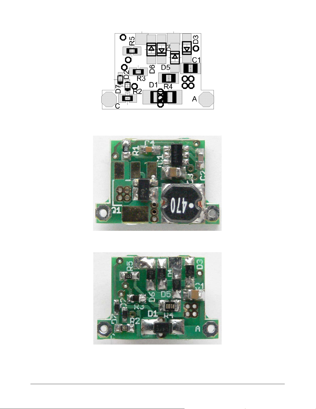
MR 16 Evaluation Board Information
A specific two sided demo board was designed to fit with
the MR 16 form factor. The schematic is almost the same for
both, but the PWM dimming control circuitry has been
removed. If the same components are used, the operation
frequency will be slightly higher due to the lower pin
capacitance because the dimming transistor contribution is
removed.
http://onsemi.com
19
Page 20
NCL30100
X2
X3
12 V
D3
D4
D5
D6
C1
R3
R5
C2
R4
NCL30100
CS
DRV
GND
VCC
CT
IVC
C4
D7
R1
R2
C3
D2
D1
L1
Q1
A
K
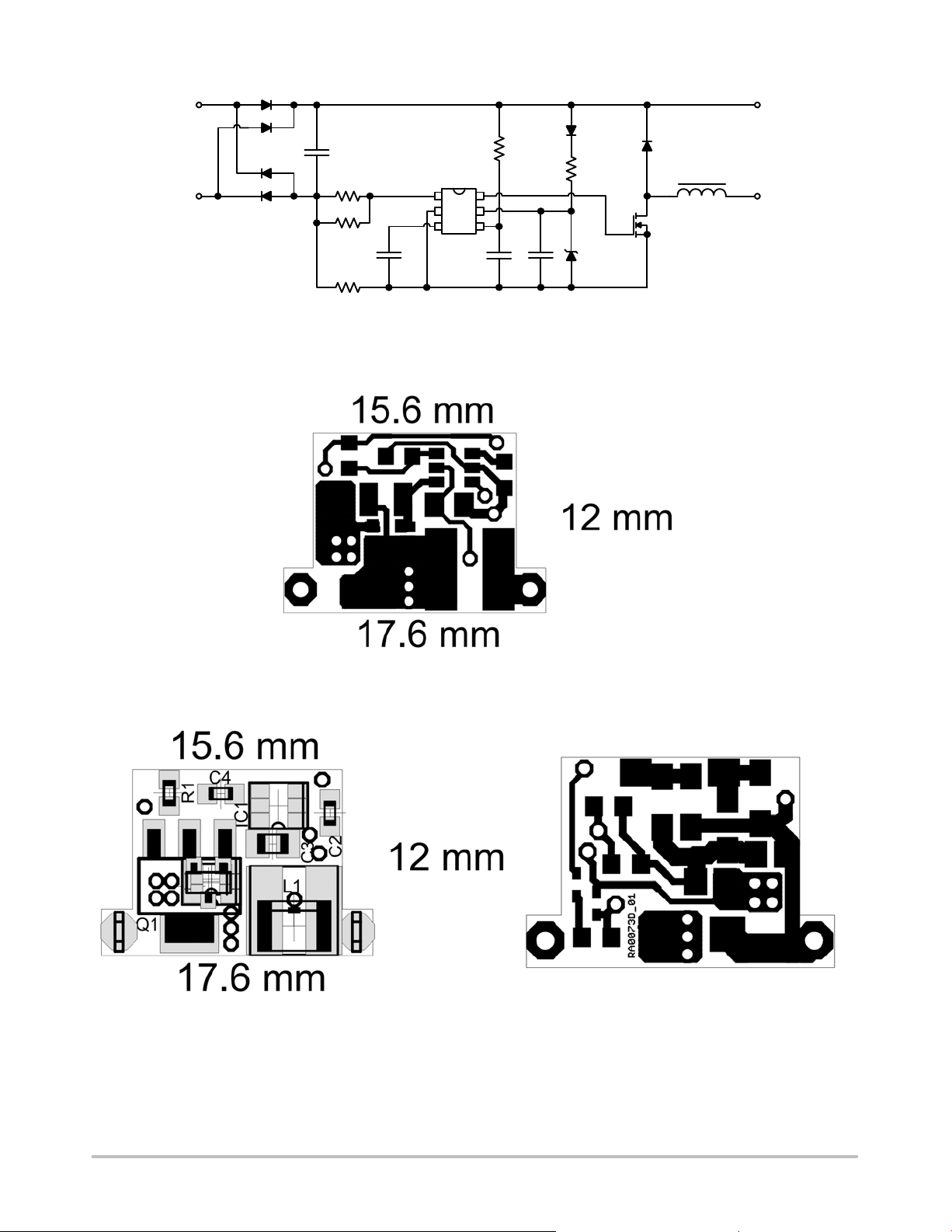
Figure 41. Schematic MR 16 Application
Figure 42. PCB Top Side MR 16 Application
Figure 43. PCB Top Side Devices Placement Figure 44. PCB Bottom Side MR 16 Application
http://onsemi.com
20
Page 21
NCL30100
Figure 45. PCB Bottom Side Devices Placement
Figure 46. Top Side Photo
Figure 47. Bottom Side Photo
http://onsemi.com
21
Page 22

NCL30100
BILL OF MATERIALS FOR THE MR 16 EVALUATION BOARD (NCL30100ADLMGEVB)
Des-
ignat-
or
C1 1 Capacitor
C2 1 Capacitor 33 pF 5% 0603 Kemet C0603C330J5GACTU Ye s Ye s
C3 1 Capacitor
C4 1 Capacitor 1 nF 10% 0603 Kemet C0603C104K5RACTU Ye s Yes
D1 1 Surface
D2 1 Zener
D3,
D4,
D5,
D6
D7 1 Schottky
IC1 1 LED
L1 1 Inductors
Q1 1 Power
Q1 1 Power
Q1 1 Power
Q1 1 Power
R1 1 Resistor 1.5 M 1% 0603 Rohm Semiconductor MCR03EZPFX1504 Ye s Ye s
R2 1 Resistor 300 R 1% 0603 Rohm Semiconductor MCR03EZPFX3000 Ye s Ye s
R3 1 Resistor 30 k 1% 0603 Rohm Semiconductor MCR03EZPFX3002 Ye s Ye s
R4 1 Resistor 0.1 R 1% 0805 Welwyn LRCS0805−0R1FT5 Yes Yes
R5 1 Resistor 2.7 k 1% 0603 Rohm Semiconductor MCR03EZPFX2701 Ye s Yes
Descrip-
Qty
tion
Mount
Schottky
Power
Rectifier
Diode
4 Schottky
Diode
Diode
Driver
MOSFET
MOSFET
MOSFET
MOSFET
Manufacturer
Value Tol Footprint Manufacturer
2.2 mF / 25 V
4.7 mF / 25 V
MBR130T3G − SOD−123 ON Semiconductor MBR130T3G No Ye s
16 V 5% SOD−523 ON Semiconductor MM5Z16VT1G No Ye s
NSR0340HT1G − SOD−323 ON Semiconductor NSR0340HT1G No Ye s
NSR0520V2T1G − SOD−523 ON Semiconductor NSR0520V2T1G No Ye s
NCL30100 − TSOP−6 ON Semiconductor NCL30100SNT1G No Yes
47 mH
NTGS4141NT1G − TSOP−6 ON Semiconductor NTGS4141NT1G No Ye s
NU − SOT−223 ON Semiconductor NTF3055−100T1G No Yes Option
NU − SOT−363 ON Semiconductor NTJS4160NT1G No Ye s Option
NU − SOT−23 ON Semiconductor NTR4170NT1G No Ye s Option
10% 0805 AV X 08053C225KAT2A Ye s Yes
10% 0805 AV X 08053D475KAT2A Ye s Yes
10% WE−PD2_M Wurth Electronik 744774147 No Ye s
Part Number
Substitution
Allowed
Pb−Free
Com-
ments
Application Design Example for an Offline (115 Vac) Buck Application:
In addition to traditional DC−DC applications, the NCL30100 can also be used in offline applications, a schematic and PCB
layout are provided to illustrate a typical circuit configuration.
• Input voltage: V
− 115 Vac
in
• Nominal LED current: 700 mA (rms)
• LED
• V
LED
• Freewheel diode V
: 120 mA (peak−to−peak)
ripple
: 3.2 V
: 0.5 V
f
• Target Switching Frequency: 50 kHz
Dimming using PWM signal 1 kHz with duty cycle 0 – 99%
In this application example, there is schematic and PCB only. The design steps are the same as above mentioned.
http://onsemi.com
22
Page 23
NCL30100
Vac
Vac
CX1
2.2n
D1
MRA4003
D3
MRA4003
D4
MRA4003
D6
MRA4003
DIMM
0/5 V
L1
100u
R3
150k
R4
5.6k
R5
R33
2.2u
5.6k
C1
C4
C3
560p10p
R6
R7
10k
Q2
BC817−16L
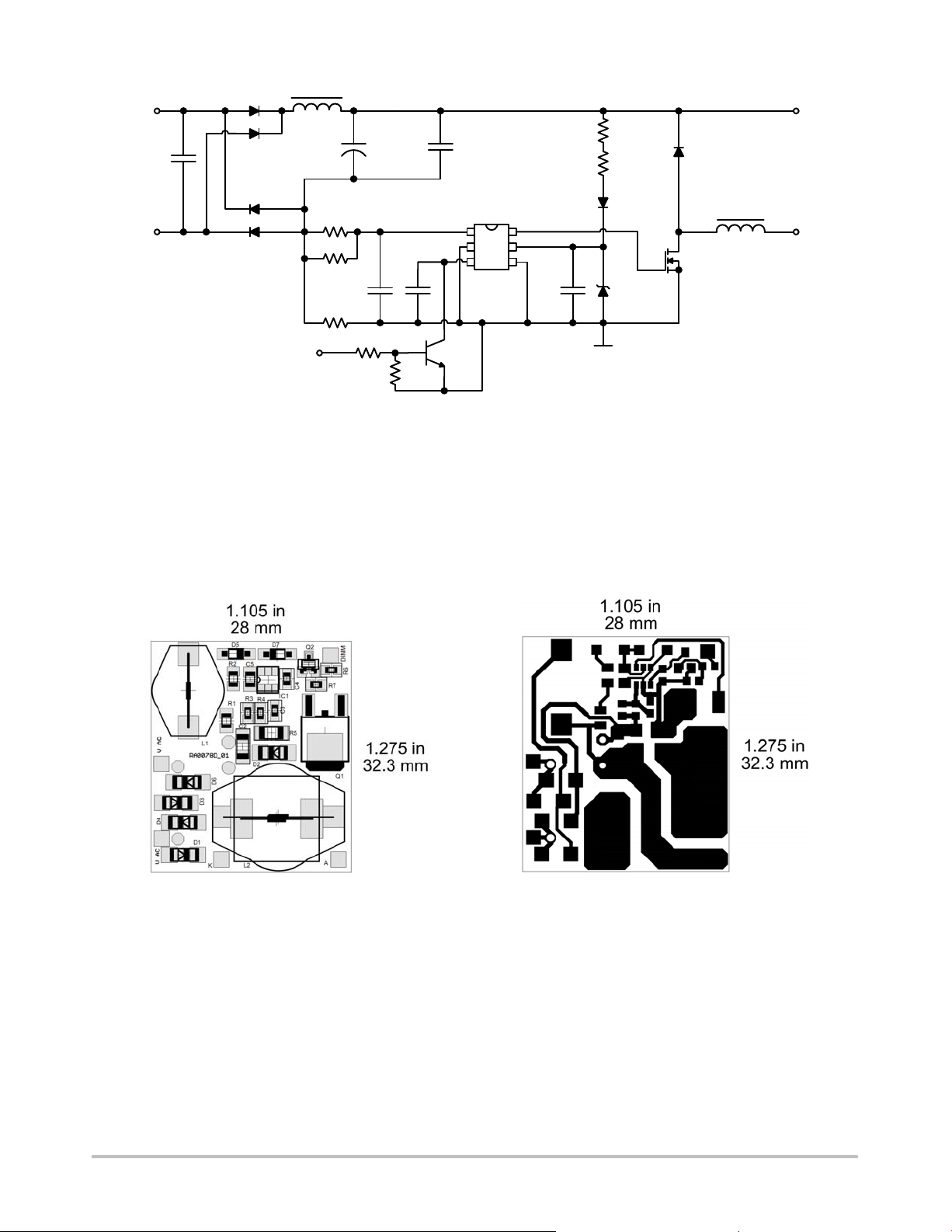
Figure 48. Design Example Schematic of 115 Vac Converter
The input voltage in range 85−140 Vac is rectified by
bridge rectifier D1, D3, D4 and D6. To limit current peaks
generated during on time period, capacitor C1 is used. CX1,
C2 and L1 are an EMI filter to protect mains against current
spikes mainly generated by D2 if Q1 is turned on. The
NCL30100 is powered through resistors R1 and R2. The
Vcc voltage is limited by D7. Maximum LED current is set
R1
C2
47n
NCL30100
CS
GND
CT
IC1
DRV
VCC
24k
R2
24k
D5
1N4148
IVC
C5
1u
GND
16V
D7
Q1
D2
MURA130
MTD6N20ET
L2
1mH
by resistors R3, R4 and R5. In this case Rsense is 0.33 W to
reach higher accuracy. A small capacitor C3 is used to filter
out spikes which are generated during the turn off of diode
D2. It is recommended to use L2 with low series resistance
since current is flowing through the inductor continuously
and D2 should be selected for low forward voltage drop and
fast reverse recovery time.
A
K
Figure 49. Component Side Figure 50. Single Layer PCB
Design for this Application
http://onsemi.com
23
Page 24
NCL30100
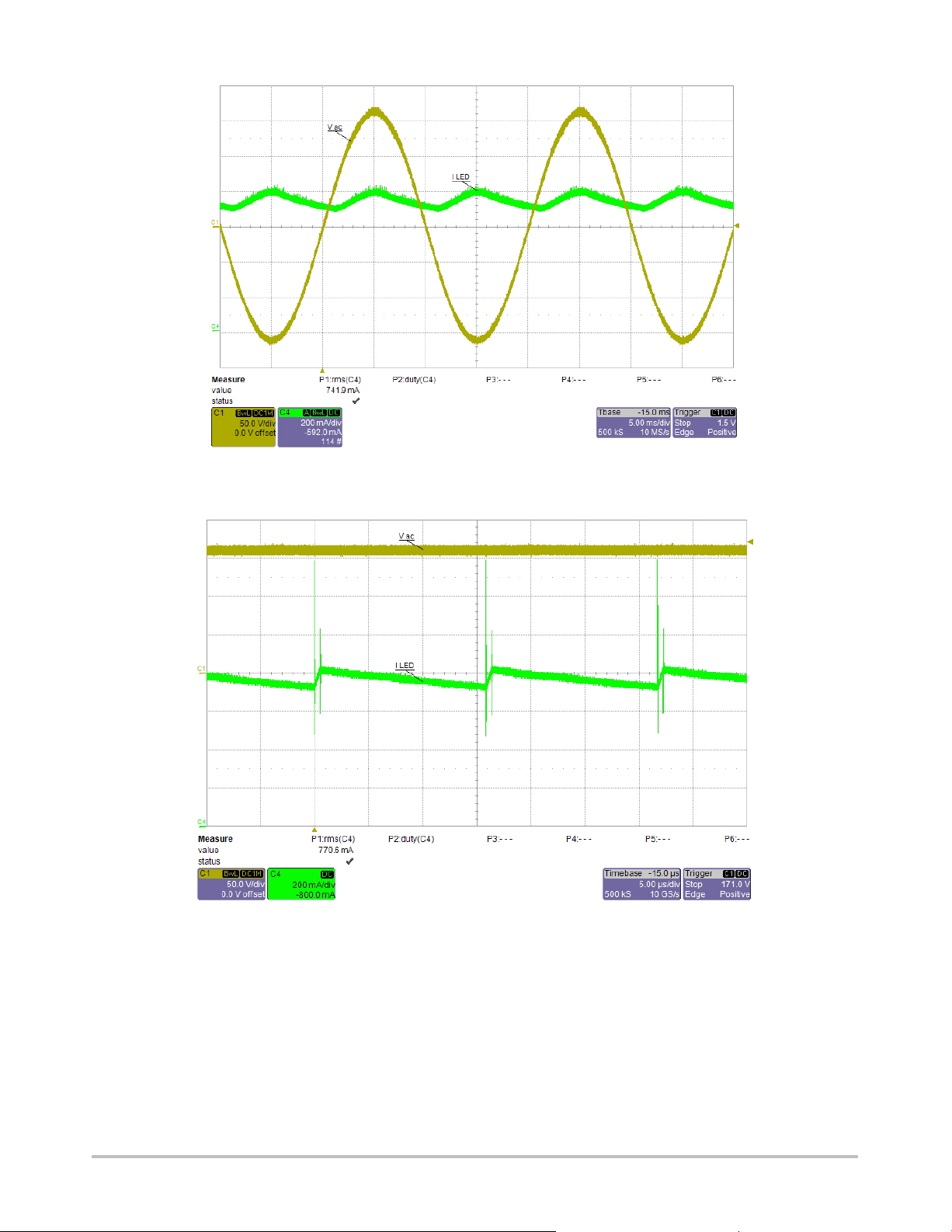
Figure 51. ILED and Vin Waveform
Figure 52. ILED at the Peak of Sinusoidal Voltage
http://onsemi.com
24
Page 25
NCL30100
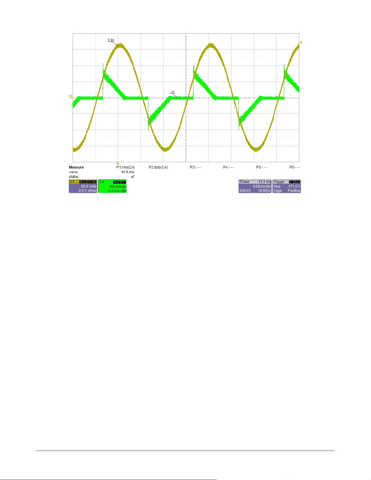
Figure 53. Input Voltage and Input Current
http://onsemi.com
25
Page 26

NCL30100
BILL OF MATERIALS FOR THE NCL30100 115 Vac
Des-
ignat-
or
Qty Description Value Tol Footprint Manufacturer
C1 1 Capacitor
C2 1 Capacitor 47 nF 10% 1206 Yageo CC1206KKX7RABB473 Yes Ye s
C3 1 Capacitor 10 pF 5% 0603 Kemet C0603C100J5GACTU Ye s Ye s
C4 1 Capacitor 560 pF 5% 0603 Kemet C0603C561J5GACTU Ye s Yes
C5 1 Capacitor
D1,
4 Standard
D3,
D4,
D6
D2 1 Ultrafast
D5 1 Standard
D7 1 Zener Diode 16 V 5% SOD−123 ON Semiconductor MMSZ16VT1G No Ye s
IC1 1 LED Driver NCL30100 − TSOP−6 ON Semiconductor NCL30100SNT1G No Ye s
L1 1 Inductors
L2 1 Inductors 1 mH 10% WE−PD_XXL Wurth Electronik 7447709102 No Ye s
Q1 1 Power
Q2 1 General
Q2 1 Power
R1,R22 Resistor 24 k 1% 0806 Rohm Semiconductor MCR06EZPFX2402 Ye s Yes
Recovery
Power
Rectifier
Power
Rectifier
Diode
MOSFET
Purpose
Transistor
NPN
MOSFET
2.2 mF / 200 V
1 mF / 25 V
MRA4003T3G − SMA ON Semiconductor MRA4003T3G No Yes
MURA130T3G − SMA ON Semiconductor MURA130T3G No Yes
MMSD4148 − SOD−123 ON Semiconductor MMSD4148T1G No Ye s
100 mH
MTD6N20 − DPAK ON Semiconductor MTD6N20ET4G No Ye s
BC817−16 − SOT−23 ON Semiconductor BC817−16LT1G No Yes
NU − SOT−23 ON Semiconductor NTS4001NT1G No Ye s Option
10% E3.5−8 Koshin KR1 2.2u 200V 8X11.5 Ye s Yes
10% 0805 AV X 08053D105KAT2A Ye s Ye s
10% WE−PD4_L Wurth Electronik 7445620 No Ye s
Manufacturer
Part Number
Substitution
Allowed
Pb−Free
Com-
ments
R3 1 Resistor 150 k 1% 0603 Rohm Semiconductor MCR03EZPFX1503 Yes Ye s
R4,R62 Resistor 5.6 k 1% 0603 Rohm Semiconductor MCR03EZPFX5601 Yes Yes
R5 1 Resistor 0.33 R 1% 0805 Welwyn LRCS0805−0R33FT5 Ye s Yes
R7 1 Resistor 10 k 1% 0603 Rohm Semiconductor MCR03EZPFX1002 Ye s Yes
CX1 1 EMI
Suppression
Capacitor
2.2 nF / 300 V 20% XC10B5 Epcos B32021A3222M289 Ye s Ye s
http://onsemi.com
26
Page 27
NCL30100
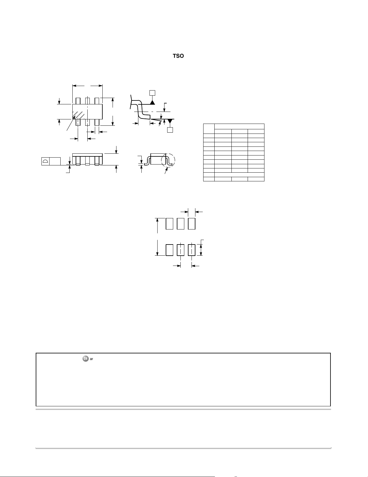
PACKAGE DIMENSIONS
TSOP−6
CASE 318G−02
ISSUE U
E1
NOTE 5
0.05
A1
D
H
456
E
23
1
b
e
A
L
DETAIL Z
c
M
DETAIL Z
L2
GAUGE
PLANE
C
SEATING
PLANE
NOTES:
1. DIMENSIONING AND TOLERANCING PER ASME Y14.5M, 1994.
2. CONTROLLING DIMENSION: MILLIMETERS.
3. MAXIMUM LEAD THICKNESS INCLUDES LEAD FINISH. MINIMUM
LEAD THICKNESS IS THE MINIMUM THICKNESS OF BASE MATERIAL.
4. DIMENSIONS D AND E1 DO NOT INCLUDE MOLD FLASH,
PROTRUSIONS, OR GATE BURRS. MOLD FLASH, PROTRUSIONS, OR
GATE BURRS SHALL NOT EXCEED 0.15 PER SIDE. DIMENSIONS D
AND E1 ARE DETERMINED AT DATUM H.
5. PIN ONE INDICATOR MUST BE LOCATED IN THE INDICATED ZONE.
DIMAMIN NOM MAX
A1 0.01 0.06 0.10
b 0.25 0.38 0.50
c 0.10 0.18 0.26
D 2.90 3.00 3.10
E 2.50 2.75 3.00
E1
e 0.85 0.95 1.05
L 0.20 0.40 0.60
L2
M
MILLIMETERS
0.90 1.00 1.10
1.30 1.50 1.70
0.25 BSC
0° 10°
−
RECOMMENDED
SOLDERING FOOTPRINT*
6X
0.60
3.20
6X
0.95
0.95
PITCH
DIMENSIONS: MILLIMETERS
*For additional information on our Pb−Free strategy and soldering
details, please download the ON Semiconductor Soldering and
Mounting Techniques Reference Manual, SOLDERRM/D.
ON Semiconductor and are registered trademarks of Semiconductor Components Industries, LLC (SCILLC). SCILLC reserves the right to make changes without further notice
to any products herein. SCILLC makes no warranty, representation or guarantee regarding the suitability of its products for any particular purpose, nor does SCILLC assume any liability
arising out of the application or use of any product or circuit, and specifically disclaims any and all liability, including without limitation special, consequential or incidental damages.
“Typical” parameters which may be provided in SCILLC data sheets and/or specifications can and do vary in different applications and actual performance may vary over time. All
operating parameters, including “Typicals” must be validated for each customer application by customer’s technical experts. SCILLC does not convey any license under its patent rights
nor the rights of others. SCILLC products are not designed, intended, or authorized for use as components in systems intended for surgical implant into the body, or other applications
intended to support or sustain life, or for any other application in which the failure of the SCILLC product could create a situation where personal injury or death may occur. Should
Buyer purchase or use SCILLC products for any such unintended or unauthorized application, Buyer shall indemnify and hold SCILLC and its officers, employees, subsidiaries, affiliates,
and distributors harmless against all claims, costs, damages, and expenses, and reasonable attorney fees arising out of, directly or indirectly, any claim of personal injury or death
associated with such unintended or unauthorized use, even if such claim alleges that SCILLC was negligent regarding the design or manufacture of the part. SCILLC is an Equal
Opportunity/Affirmative Action Employer. This literature is subject to all applicable copyright laws and is not for resale in any manner.
PUBLICATION ORDERING INFORMATION
LITERATURE FULFILLMENT:
Literature Distribution Center for ON Semiconductor
P.O. Box 5163, Denver, Colorado 80217 USA
Phone: 303−675−2175 or 800−344−3860 Toll Free USA/Canada
Fax: 303−675−2176 or 800−344−3867 Toll Free USA/Canada
Email: [email protected]
N. American Technical Support: 800−282−9855 Toll Free
USA/Canada
Europe, Middle East and Africa Technical Support:
Phone: 421 33 790 2910
Japan Customer Focus Center
Phone: 81−3−5773−3850
http://onsemi.com
ON Semiconductor Website: www.onsemi.com
Order Literature: http://www.onsemi.com/orderlit
For additional information, please contact your local
Sales Representative
NCL30100/D
27
Page 28

 Loading...