

Page 1
Quasi-Resonant Buck
l
Controller for Precise
Current Regulation and
Wide Analog Dimming
NCL30076
The NCL30076 is a DC−DC buck controller for wide dimming
range down to 1% by analog dimming control to relieve audible noise
and flicker in PWM dimming. ON Semiconductor’s proprietary LED
current calculation technique driven by zero input offset amplifiers
performs precise constant current in the whole analog dimming range.
Multi−mode operation provides high efficiency with minimized
switching loss by QR at heavy load and deep analog dimming by DCM
at light load.
PWM dimming control is also provided in case that constant LED
color temperature is required. The NCL30076 has several protections
such as LED short protection, over current protection, thermal
shutdown and VDD over voltage protection for robust system
reliability.
Features
• Wide Analog Dimming Range: 1~100%
• Low CC Tolerance: ±2% at 100% Load & ±20% at 1% Load
• Low System BOM
• LED Off Mode at Standby
• Low Standby Current
• PWM Dimming Available
• Gate Sourcing and Sinking Current of 0.5 A/0.8 A
• Robust Protection Features
♦ LED Short Protection
♦ Over Current Protection
♦ Thermal Shutdown
♦ V
Over Voltage Protection
DD
Typical Applications
• LED Lighting System
www.onsemi.com
8
1
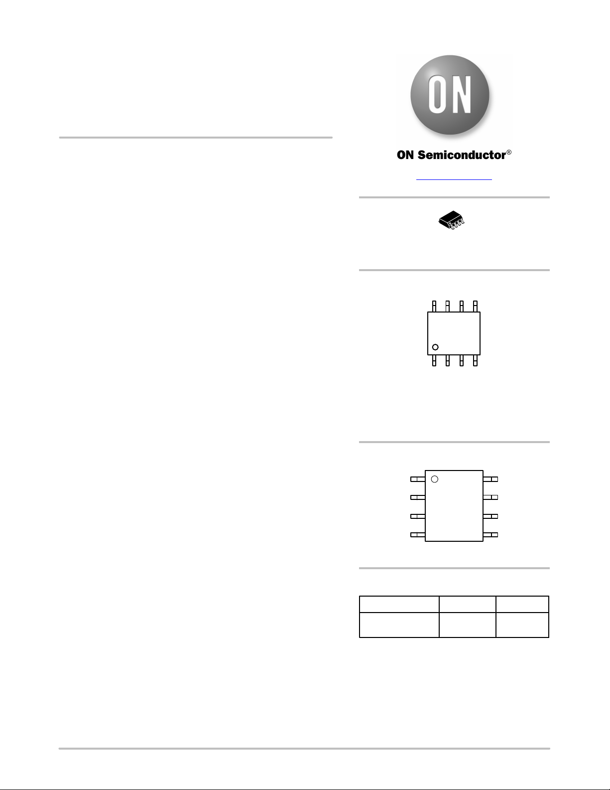
SOIC−8 NB
CASE 751
MARKING DIAGRAM
L30076AA
AWLYYWW
L30076 = Specific Device Code
AA = Default Trimming Option
A = Assembly Location
WL = Wafer Lot Traceability Code
YYWW = 4 Digit Data Code
PIN ASSIGNMENT
PGBIAS
DRVCSZCD
VDDSG
DIMFB
(Top View)
© Semiconductor Components Industries, LLC, 2020
April, 2021 − Rev. 3
ORDERING INFORMATION
Device Package Shipping
NCL30076AADR2G SOIC−8 NB 3000 /
Tape & Ree
†For information on tape and reel specifications,
including part orientation and tape sizes, please
refer to our Tape and Reel Packaging Specification
Brochure, BRD8011/D.
1 Publication Order Number:
NCL30076/D
Page 2
NCL30076
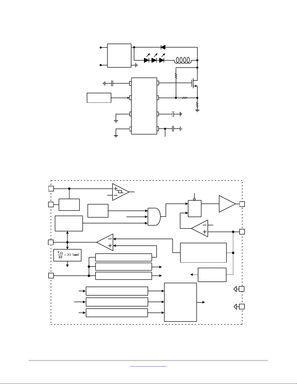
APPLICATION SCHEMATIC
200~500 Vin
VDD
BIAS
FB
3.3 V
LDO
T
OF F.FB
generator
V
FB
V
AC
Dimming
Signal
10 V /
8 V
Soft
Start
OTA
PFC
Stage
FB
DIM
NCL30076
SG
BIAS
PG
External source
Figure 1. Application Schematic
BLOCK DIAGRAM
V
DD−ON
V
TO FF.SS
V
TO FF.ZCD
V
TO FF.FB
V
LED
V
REF
Reference control
DRV
CSZCD
VDD
|| V
V
PDIM
V
ON
S
V
OF F
R
Precise LED
current calculator
RCS
SHUTDOWN
Q
V
PWM
V
CS.LIM
DRV
CSZCD
DIM
V
V
CSZCD
CS.LIM
PWM dimming control
Standby mode control
V
DD
Over voltage protection
Over current protection
T
J
Thermal Shutdown
V
PDIM
V
SHUTDOWN
Protection
AR control
V
TO FF.ZCD
ZCD
detector
V
SHUTDOWN
PG
SG
Figure 2. Simplified Block Diagram
www.onsemi.com
2
Page 3
NCL30076
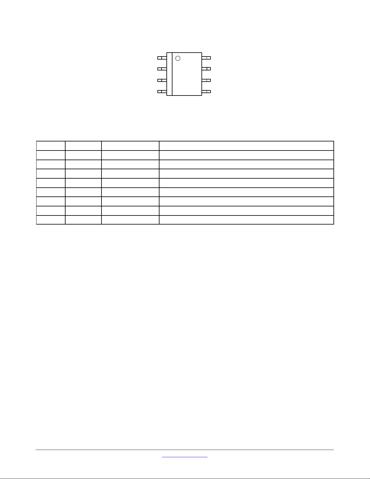
PIN FUNCTION DESCRIPTION
Pin No.
Pin Name
Function
Description
1
BIAS
3.3 V BIAS
This pin is 3.3 V LDO output to bias the internal digital circuit
2
CSZCD
CS and ZCD Sensing
This pin detects the switch current and the inductor current zero cross time
3SGSignal Ground
Signal Ground is close to control pin circuit such as CSZCD, DIM and FB
4FBFeedback
Output of feedback OTA
5
DIM
Dimming Input
Dimming signal is provided to this pin
6
VDD
Power Supply
IC operating current is supplied to this pin
7
DRV
Output Drive
This pin is connected to drive external switch
8PGPower Ground
Power Ground is close to the capacitors at BIAS and VDD pin
PIN CONFIGURATION
(Top View)
Figure 3. Pin Configuration
PGBIAS
DRVCSZCD
VDDSG
DIMFB
www.onsemi.com
3
Page 4
NCL30076
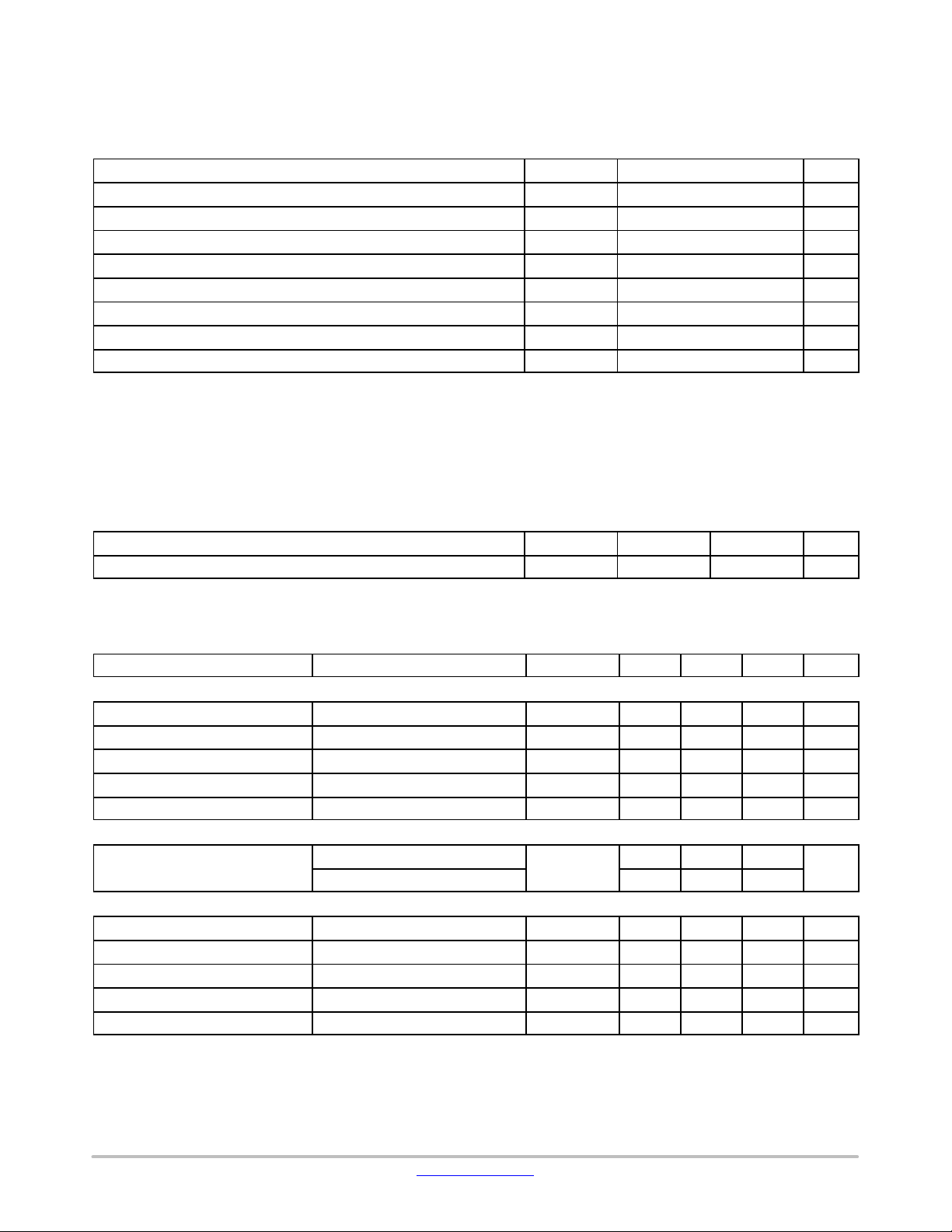
MAXIMUM RATINGS
Parameter
Symbol
Value
Unit
VDD, DRV Pin Voltage Range
V
−0.3 to 30
V
DIM, FB, CSZCD, BIAS Pin Voltage Range
V
−0.3 to 5.5
V
Maximum Power Dissipation (TA < 50°C)
P
550
mW
Maximum Junction Temperature
T
150
C
Storage Temperature Range
T
−55 to 150
C
Junction−to−Ambient Thermal Impedance
R
145
C/W
ESD Capability, Human Body Model (Note 2)
ESD
2
kV
ESD Capability, Charged Device Model (Note 2)
ESD
1
kV
RECOMMENDED OPERATING RANGES
Parameter
Symbol
Min
Max
Unit
Junction Temperature
TJ−40
125
C
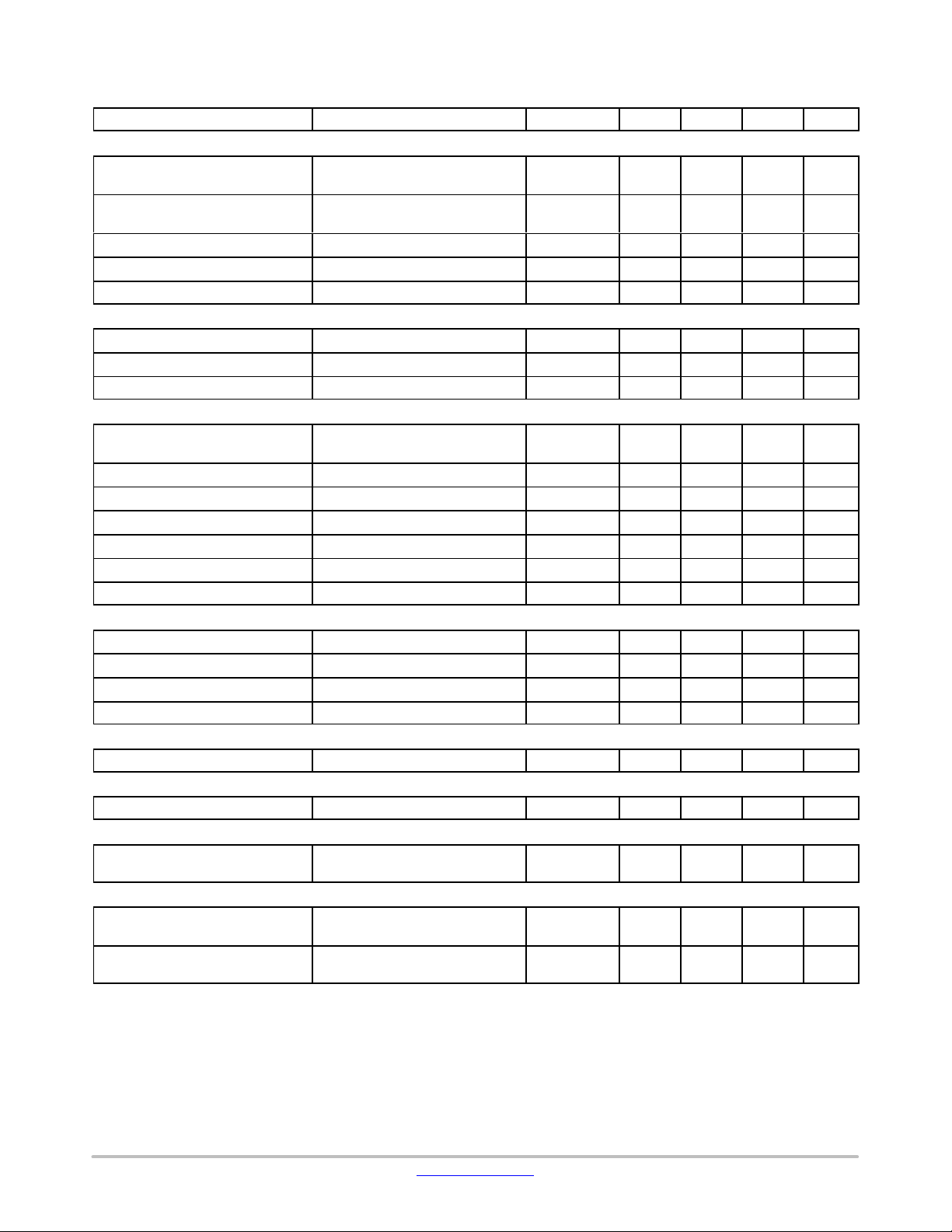
ELECTRICAL CHARACTERISTICS (V
= 15 V and TJ = −40~125°C unless otherwise specified)
Parameter
Test Conditions
Symbol
Min
Typ
Max
Unit
VDD SECTION
IC Turn−On Threshold Voltage
V
9.3
10.0
10.7
V
IC Turn−Off Threshold Voltage
V
7.4
8.0
8.6
V
Startup Current
VDD = V
− 1.6 V
I
−
250
400
A
Operating Current
I
−
6.5
8.0
mA
Standby Current
I
−
200
300
A
BIAS SECTION
3.23
3.30
3.37
TJ = 25~100°C (Note 4)
3.25
3.30
3.35
DIM SECTION
DIM Voltage for 100% V
V
= 1.9 V
V
)
1.755
1.80
1.845
V
DIM Voltage for 99% V
V
)
1.730
1.78
1.827
V
Standby Enabling DIM Voltage
V
5075100
mV
Standby Disabling DIM Voltage
V
60
100
140
mV
Standby Delay Time
t
91011
ms
SPECIFICATIONS
MV(MAX)
LV(MAX)
D(MAX)
J(max)
STG
θJA
HBM
CDM
Stresses exceeding those listed in the Maximum Ratings table may damage the device. If any of these limits are exceeded, device functionality
should not be assumed, damage may occur and reliability may be affected.
1. Refer to ELECTRICAL CHARACTERISTICS, RECOMMENDED OPERATING RANGES and/or APPLICATION INFORMATION for Safe
Operating parameters.
2. This device series incorporates ESD protection and is tested by the following methods:
− ESD Human Body Model per JEDEC Standard JESD22−A114
− ESD Charged Device Model per JEDEC Standard JESD22−C101
− Latch−up Current Maximum Rating ±100 mA per JEDEC Standard JESD78
°
°
°
°
Functional operation above the stresses listed in the Recommended Operating Ranges is not implied. Extended exposure to stresses beyond
the Recommended Operating Ranges limits may affect device reliability.
DD
DD(ON)
DD(OFF)
DD(ON)
BIAS Voltage V
REF
REF
DIM
DIM(REF−MAX
DIM(MAX−EFF
DIM(SB−ENA)
DIM(SB−DIS)
SB(DELAY)
DD(ST)
DD(OP)
DD(SB)
BIAS
m
m
V
www.onsemi.com
4
Page 5
NCL30076
E
FB SECTION
FB OTA Source Current
IFB = (V
− V
) x g
x 10
I
−14.0
−11.5
−9.0
A
FB OTA Sink Current
IFB = (V
− V
) x g
x 10
I
9.0
11.5
14.0
A
FB OTA Transconductance
g
= IFB / {(V
− V
) x 10}
g
182328
mho
FB OTA High Voltage
V
= 150 mV, V
= 100 mV
V
4.7−−
V
FB Minimum Clamping Voltage
V
= 0 mV, V
= 100 mV
V
0.4
0.5
0.6
V
CS SECTION
CS Regulation
V
)
155
160
165
mV
CS Current Limit Maximum
V
390
410
430
mV
CS Current Limit Minimum
V
145
155
165
mV
DUTY SECTION
Leading Edge Blanking Time at
t
360
400
440
ns
Maximum Ton Time
t
455055
s
Minimum Toff Time
VFB = 3.8 V
t
900
1250
1500
ns
Maximum Toff Time
VFB = 0.5 V
t
1.17
1.30
1.43
ms
Maximum FB Voltage for Min. Toff
V
)
3.30
3.43
3.55
V
Minimum FB Voltage for Max. Toff
V
)
0.9
1.1
1.3
V
Quasi−Resonant Delay Time
tQR0.45
0.50
0.55
s
DRV SECTION
DRV Low Voltage
V
−−0.2
V
DRV High Voltage
VDD = 15 V
V
111213
V
DRV Rising Time
C
= 3.3 nF
t
60
100
145
ns
DRV Falling Time
C
= 3.3 nF
t
2555105
ns
AUTO RESTART SECTION
Auto Restart Time at Protection
t
0.9
1.0
1.1
s
VDD OVER VOLTAGE PROTECTION SECTION
VDD Over Voltage Threshold Voltage
V
222324
V
OVER CURRENT PROTECTION SECTION
CS Over Current Protection
V
0.9
1.0
1.1
V
THERMAL SHUTDOWN SECTION
Thermal Shut Down Temperature
TSD130
150
170°C
Thermal Shut Down Hysteresis
T
253035°C
LECTRICAL CHARACTERISTICS (V
Parameter UnitMaxTypMinSymbolTest Conditions
Turn−on
= 15 V and TJ = −40~125°C unless otherwise specified) (continued)
DD
LED
REF
V
= 150 mV, V
REF
V
= 50 mV, V
REF
M(FB)
REF
REF
LED
LED
REF
LED
REF
LED
LED
M(FB)
= 100 mV
M(FB)
= 100 mV
LED
FB(SOURCE)
FB(SINK)
M(FB)
FB(HIGH)
FB(CLP)
CS(REG−MAX
CS(LIM−MAX)
CS(LIM−MIN)
LEB(TON)
ON(MAX)
OFF(MIN)
OFF(MAX)
FB(MAX−TOFF
FB(MIN−TOFF
m
m
m
m
m
DRV(LOW)
DRV(HIGH)
DRV
DRV
Threshold
DRV(R)
DRV(F)
AR(PROT)
DD(OVP)
CS(OCP)
(Note 3)
(Note 3)
SD(HYS)
Product parametric performance is indicated in the Electrical Characteristics for the listed test conditions, unless otherwise noted. Product
performance may not be indicated by the Electrical Characteristics if operated under different conditions.
3. Guaranteed by design.
4. Guaranteed by characterization.
www.onsemi.com
5
Page 6
NCL30076
1.006
1.006
CS(LIM−MIN)
DD(OVP)
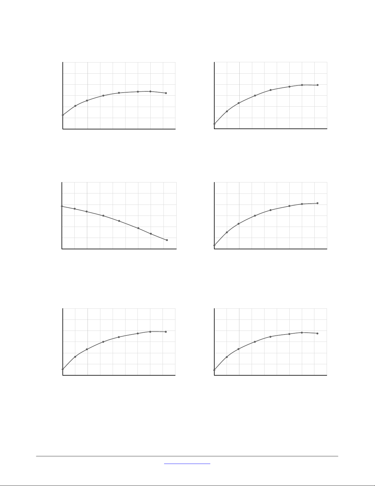
TYPICAL CHARACTERISTICS
(These characteristic graphs are normalized at TA = 25°C)
1.004
1.002
1
0.998
Normalized at 255C
0.996
0.994
−40 −20 0 20 40 60 80 100 120 140
Temperature (5C)
Figure 4. V
1.03
1.02
1.01
1
0.99
Normalized at 255C
0.98
0.97
−40 −20 0 20 40 60 80 100 120 140
vs. Temperature Figure 5. V
BIAS
Temperature (5C)
1.004
1.002
1
0.998
Normalized at 255C
0.996
0.994
−40 −20 0 20 40 60 80 100 120 140
Temperature (5C)
DIM(MAX)
1.006
1.004
1.002
1
0.998
Normalized at 255C
0.996
0.994
−40 −20 0 20 40 60 80 100 120 140
vs. Temperature
Temperature (5C)
Figure 6. g
1.006
1.004
1.002
1
0.998
Normalized at 255C
0.996
0.994
−40 −20 0 20 40 60 80 100 120 140
vs. Temperature Figure 7. V
M(FB)
Temperature (5C)
Figure 8. V
vs. Temperature Figure 9. V
CS(REG−MAX)
1.006
1.004
1.002
1
0.998
Normalized at 255C
0.996
0.994
−40 −20 0 20 40 60 80 100 120 140
vs. Temperature
Temperature (5C)
vs. Temperature
www.onsemi.com
6
Page 7

NCL30076
APPLICATION INFORMATION
General
NCL30076 provides wide analog dimming down to 1%
with accurate CC regulation. According to buck inductor,
input voltage and output voltage, deep dimming down to
0.1~0.2% load can be achieved. Thanks to
ON Semiconductor’s proprietary LED current calculation
technique, NCL30076 is able to sense the current of LED
load connected at input voltage node with no upper limit of
the input voltage with high design flexibility and system
reliability. LED current sensed by internal zero input o ffset
amplifiers performs accurate CC regulation in the whole
analog dimming range. Therefore, CC tolerance is tightly
controlled within ±2% at 100% load and ±20% at 1% load.
Wide Analog Dimming
Wide analog dimming range is obtained by transitioning
multi−mode operation between QR and DCM according to
the dimming condition. At full load condition, QR with
valley switching minimizes switching loss for high system
efficiency and DCM is activated at light load condition to
perform deep analog dimming. Internal LED current
calculator and a digital compensator provide dimming
linearity over the entire dimming range.
PWM Dimming
Analog dimming has benefits for less audible noise and
flicker compared to PWM dimming. However, PWM
dimming method is generally required to keep the constant
LED color temperature in specific applications. NCL30076
supports PWM diming by simply providing PWM dimming
signal to DIM pin.
Precise CC Regulation
CC regulation is very important especially in
programmable LED driver system to keep constant LED
current under system variation of LED load, inductor,
temperature, etc. NCL30076 applies zero input offset
amplifiers at LED current calculator and OTA. Those blocks
can implement precise LED current sensing and FB voltage
generation.
Therefore, NCL30076 supports low CC tolerance less
than ±2% at full load and ±20% at 1% load in the system
variation.
Soft start
At startup, an internal soft start block gradually reduces
T
time from maximum T
OFF
limit so that LED current is
OFF
settled smoothly without overshoot current and unexpected
flash.
Standby Mode
When V
is lower than a standby threshold voltage for
DIM
10 ms, standby mode is triggered with LED turn−off and IC
current consumption is minimized.
Auto Restart (AR) at Protection
Once protection is triggered, IC operation stops for
1 second and begins soft start operation after the auto restart
time delay.
VDD Over Voltage Protection (OVP)
When VDD is higher than V
DD (OVP)
threshold, over
voltage protection is triggered.
Short LED Protection (SLP)
When LED is short circuited, the buck stage operates at
minimum switching frequency, so the maximum turn−off
time control protects the freewheeling diode from thermal
stress.
Over Current Protection (OCP)
When CSZCD voltage exceeds the over current threshold
voltage, switching is immediately shut down after leading
edge blanking time in the short circuit condition of the
inductor or the freewheeling diode.
Thermal Shot Down (TSD)
When IC junction temperature is higher than 150°C, TSD
is triggered and released when the temperature is lower than
120°C.
www.onsemi.com
7
Page 8
NCL30076
BASIC OPERATION
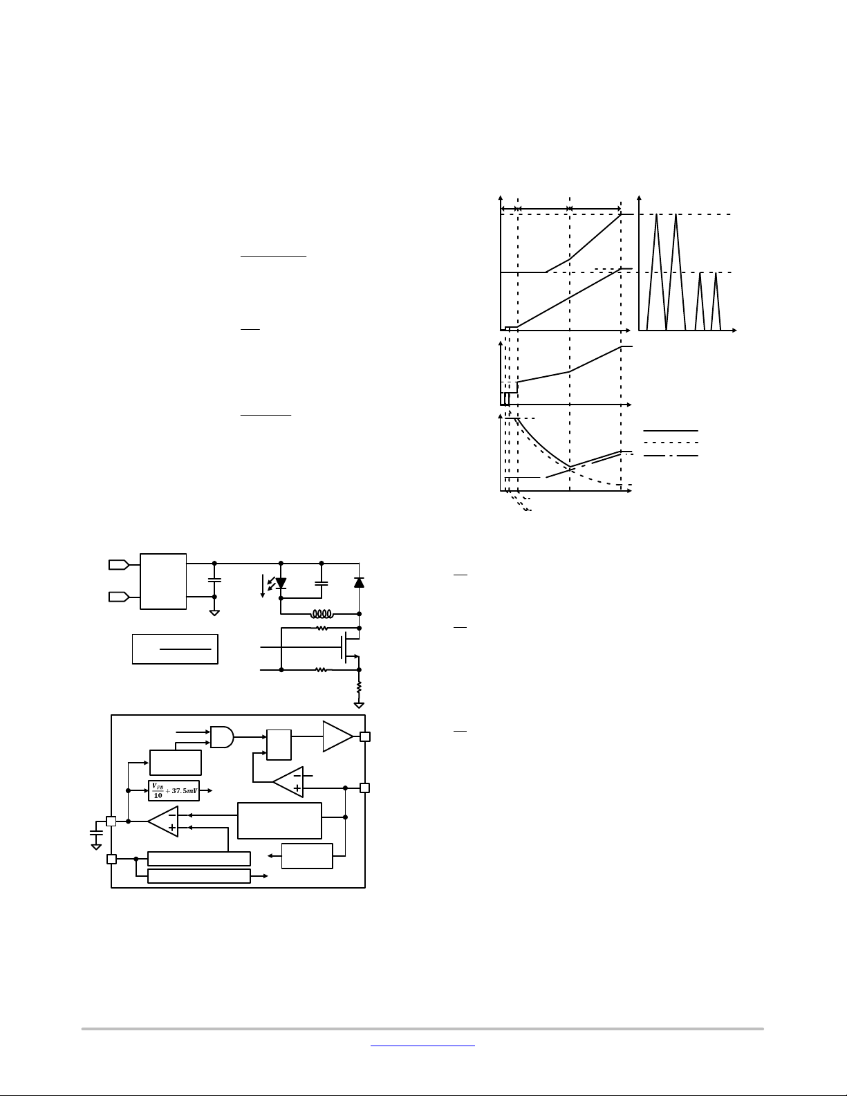
NCL30076 is the current mode buck controller in which
DRV is of f when V
CSZCD
reaches to V
by inductor current zero cross signal (V
T
generator output (V
OFF.FB
Figure 10. V
is calculated based on V
LED
) in DCM as shown in
TOFF.FB
CS.LIM
TOFF.ZCD
CSZCD
and DR V is on
) in QR and
in precise
LED current calculator block composed of zero input offset
amplifiers and V
is controlled by DIM signal by below
REF
equation.
V
* 0.2V
V
is compared with V
LED
V
sets V
FB
CS.LIM
V
VFB also controls V
in which V
TOFF.FB
[V] +
DIM
10
by OTA to generate VFB.
REF
V
REF
as below equation.
V
FB
CS.LIM
[V] +
TOFF.FB
) 37.5 mV
10
signal by T
is triggered at T
OFF.FB
OFF.FB
after DRV is
(eq. 1)
(eq. 2)
generator
turned off.
T
[ms] +
OFF.FB
When V
IC counts t
V
TOFF.ZCD
drops after the inductor current zero cross,
CSZCD
(0.5 ms) and trigger V
QR
signal is generated later than V
and DRV on is determined by V
2.7
VFB* 1.1
TOFF.ZCD
) 0.1
TOFF.FB
TOFF.ZCD
switching. In DCM mode, DRV on is set by V
T
is longer than V
OFF.FB
TOFF.ZCD
triggering time.
(eq. 3)
. In QR mode,
signal
for valley
as
TOFF.FB
Wide Analog Dimming
NCL30076 operates in QR at full load and in DCM at light
load for a wide dimming range. Figure 11 shows how
NCL30076 operates with V
B AC
~320 mV
V
155 mV
1.1 V
0.5 V
CS .LIM
V
REF
V
FB
t
OFF (MA X)
500 ms
~ 1 V
0.2 V
0.1/0.07 5 V
Figure 11. Operation Mode vs. V
DIM
16 0 mV
1.8 V
.
I
x R
LBUC K
CS
A(QR)
B(DCM)
T
OFF
T
OFF.FB
T
OFF.ZCD
t
V
DIM
V
DIM
V
DIM
DIM
DIM
FB
PFC
V
AC
Stage
I
=
LED
V
FB
OTA
C
IN
− 0.2 V
V
DIM
10 x R
CS
CSZCD
V
TO FF.ZCD
V
TO FF.FB
T
OF F.FB
generator
V
CS.LIM
V
LED
V
REF
Reference control
Standby mode control
I
LED
DRV
V
ON
Q
S
V
OF F
R
Precise LED
current calculator
V
= I
LED
LED
V
TO FF.ZCD
V
STANDBY
Figure 10. NCL30076 Block Diagram
D
LED
V
PWM
x R
CS
ZCD
detector
C
LED
D
BUCK
L
BUCK
• A: V
T
T
FB
OFF.ZCD
OFF.FB
controls V
CS.LIM
and T
with QR switching as T
.
is determined by
OFF
OFF.ZCD
is longer than
• B: Operating mode is transitioned from QR to DCM at th e
R
ZCD1
Q
BUCK
R
ZCD2
R
CS
DRV
V
CS.LIM
CSZCD
boundary between A and B region which is
approximately half load. T
as T
reduced, V
is longer than T
OFF.FB
is no longer controlled by VFB and
CS.LIM
clamped to minimum V
• C: When V
is pulled down to 0.5 V clamping voltage with min.
V
FB
is lower than 0.2 V, V
DIM
LED current under open loop control. When V
is determined by T
OFF
OFF.ZCD
CS.LIM
. When V
(155 mV).
is further
DIM
is set to 0 V and
REF
OFF.FB
is
DIM
lower than 0.075/0.1 V, standby mode is triggered with
LED turn−off.
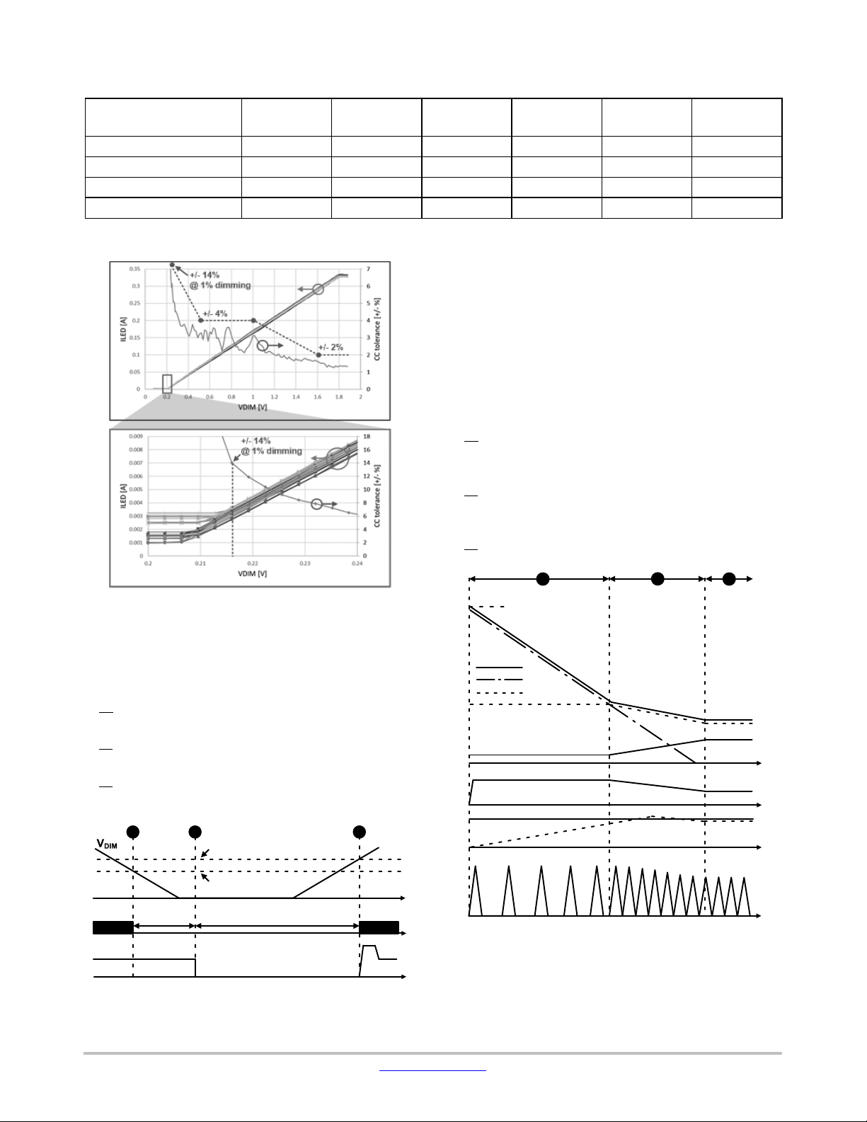
Precise CC Regulation
Current sensing amplifier and OTA applies zero input
offset compensation technique for precise CC regulation
and dimming curve linearity in multi−mode operation
Table 1 shows CC tolerance measured by changing
inductor (±15%), temperature (−10, 25, 90 °C), output
voltage (100, 200, 300 V) and controller 150 pcs (3 lot
variation) in 400 V input 100 W driver. As a result, CC
tolerance with system variables at 1% deep dimming
condition is less than ±26% and less than ±3.0% at full load
condition.
www.onsemi.com
8
Page 9
NCL30076
Table 1. CC TOLERANCE (150 pcs)
Inductor : +15%
100% Load
50% Load
10% Load
5% Load
2% Load
1% Load
V
: 100 V
1.99
3.77
4.41
5.32
9.22
16.23
V
: 200 V
1.83
3.70
4.76
5.23
8.64
14.44
V
: 300 V
1.86
3.06
4.33
5.80
10.57
20.54
*
V
: 100 / 200 / 300 V
2.29
4.10
5.45
6.94
13.48
25.38
*
Temp. : −10 / 25 / 90 5C
OUT
OUT
OUT
OUT
*The main deviation factor is high temperature condition. The Total CC tolerance at 1% deep dimming condition without high temperature
condition is less than 20%.
Soft Start
During soft start operation, Internal soft start counter
T
When T
settled to regulation level and T
T
start time, T
control anymore. Figure 14 shows how the soft start
operates at full load condition where T
as T
• A: T
• B: T
• C: V
contributes to T
OFF.SS
OFF_SS
or T
OFF.FB
is set by T
OFF
is determined by T
OFF
t
OFF(MAX)
DCM mode.
is controlled by T
OFF
than T
OFF.ZCD
falling.
is settled in regulation level and steady state starts.
FB
by reduced from t
OFF
OFF(max)
reaches to the steady state level, VFB is
is finally decided to
OFF
OFF.ZCD
by load condition. In the end of the soft
reaches to 0 and doesn’t affect T
OFF.SS
OFF.FB
OFF.ZCD
in QR mode.
which is reduced from
OFF.SS
OFF
is not engaged
. VFB is pulled up and the system operates in
. V
LED
OFF.ZCD
is closer to V
as T
REF
is shorter
OFF.SS
, and VFB starts
.
Figure 12. NCL30076 Dimming Curve and CC
Tolerance
Standby Mode
Standby mode is triggered by V
as shown in
DIM
Figure 13.
• A: When V
is lower than V
DIM
DIM(SB−ENA)
down. So, LED lamps turn off.
• B: After t
SB(DELAY)
(10 ms), standby mode is entered and
NCL30076 current consumption drops to I
• C: When V
is higher than V
DIM
DIM(SB−DIS)
mode is immediately terminated and IC starts up.
A B C
100 mV V
75 mV V
V
DRV
t
SB(DELAY)
V
FB
Figure 13. NCL30076 Standby Mode
DIM(SB−DIS)
DIM(SB−ENA)
Standby Mode
, DR V is shut
.
DD(SB)
, standby
Time
t
OFF (MAX )
1300 ms
T
OFF .FB
V
FB
V
REF
V
LED
I
LBUC K
T
OFF
T
OFF .SS
T
OFF
T
OFF .SS
T
OFF .ZCD
A
by
B
T
by
OFF
T
OFF .ZCD
(VFB falls to
steady state level)
Figure 14. Soft Start Sequence
(Full Load Startup in QR)
C
T
by
OFF
T
OFF .ZCD
(steady
state)
Time
www.onsemi.com
9
Page 10

NCL30076
Protections
• VDD Over Voltage Protection (OVP)
When VDD is higher than V
DD(OVP)
is triggered with 1 sec AR timer. Open LED protection
can be implemented by VDD OVP when VDD is supplied
by auxiliary winding in the buck inductor.
(23 V), VDD OVP
• Over Current Protection (OCP)
When CSZCD voltage is higher than V
leading edge blanking time, t
CS(OCP)
LEB(TON)
immediately shuts down with 1 sec AR timer .
(1 V) after
(400 ns), IC
• Short LED Protection (SLP)
When LED load is short−circuited, T
is lengthened to
OFF
1300 ms, t
OFF(MAX)
detection. Therefore, max. T
due to the absence of zero cross
control protects the
OFF
freewheeling diode from thermal stress and the diode
current is regulated close to the LED current set by V
• Thermal Shut Down (TSD)
When the junction temperature is higher than T
system shuts down and the junction temperature is
monitored at every 1 second AR delay time. When the
temperature is lower than T
restarts.
SD
– T
SD(HYS)
, the system
SD
DIM
, the
.
www.onsemi.com
10
Page 11
NCL30076
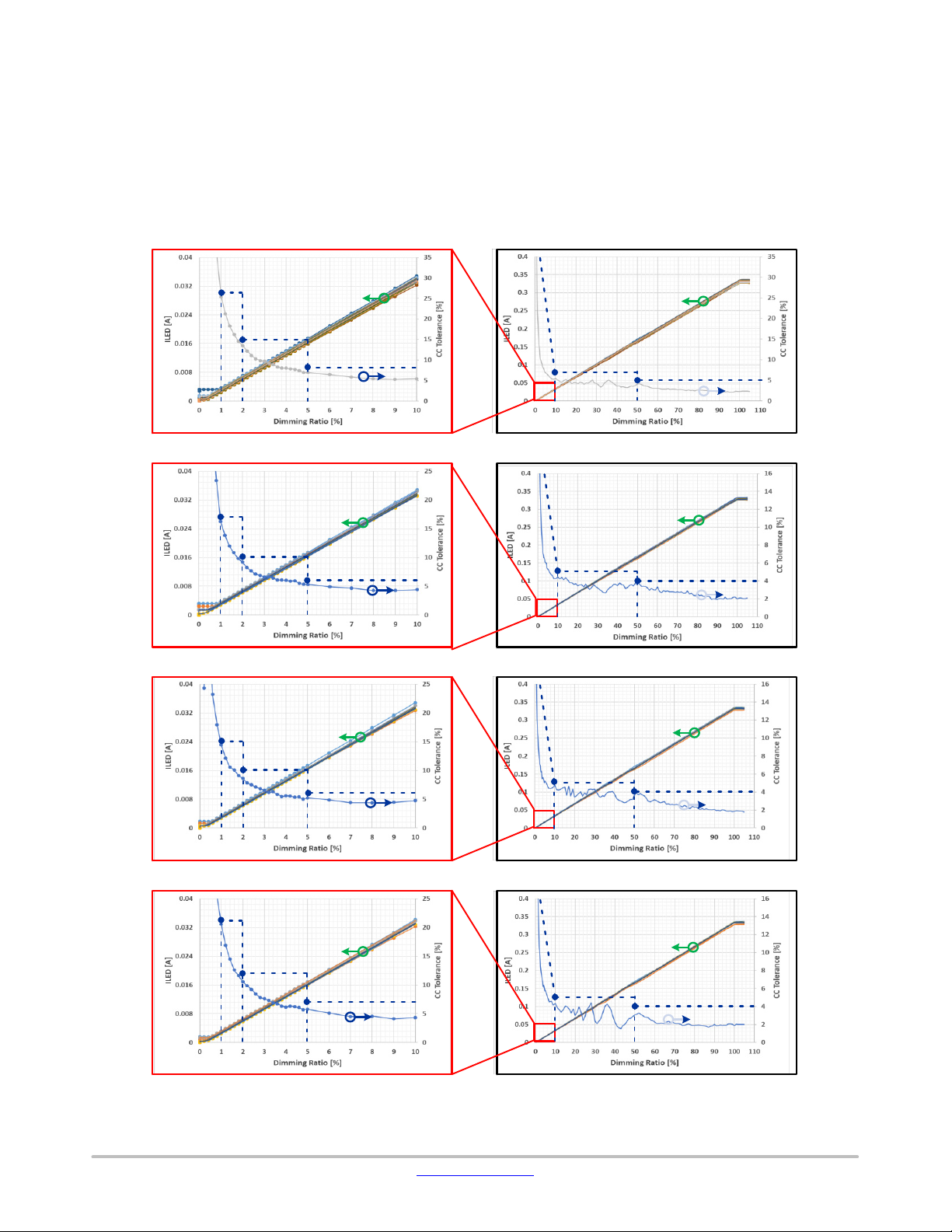
APPENDIX: DIMMING CURVE AND CC TOLERANCE WITH SYSTEM VARIABLES
− System: NCL30076 100 W (V
: 400 V / V
IN
: 100 ~ 300 V / I
OUT
− Temperature variation: −10 / 25 / 90 °C
− Inductance variation: ±15% (1.36 mH ~ 1.84 mH)
− Output Voltage: 100 / 200 / 300 V
− NCL35076 Controller: 150 pcs (3 lot variation)
Wide Output Condition (100/200/300V)
NCL30076 150pcs (3lot) + Temp & Inductor variation
+/− 26%
+/− 15%
+/− 8%
Single Output Condition (100V)
NCL30076 150pcs (3lot) + Temp & Inductor variation
+/− 17%
+/− 10%
+/− 6%
OUT(MAX)
: 333 mA)
+/− 7%
+/− 5%
+/− 5%
+/− 4%
Single Output Condition (200V)
NCL30076 150pcs (3lot) + Temp & Inductor variation
+/− 15%
+/− 10%
+/− 6%
Single Output Condition (300V)
NCL30076 150pcs (3lot) + Temp & Inductor variation
+/− 21%
+/− 12%
+/− 7%
Figure 15. CC Tolerance (150 pcs)
+/− 5%
+/− 5%
+/− 4%
+/− 4%
www.onsemi.com
11
Page 12
NCL30076
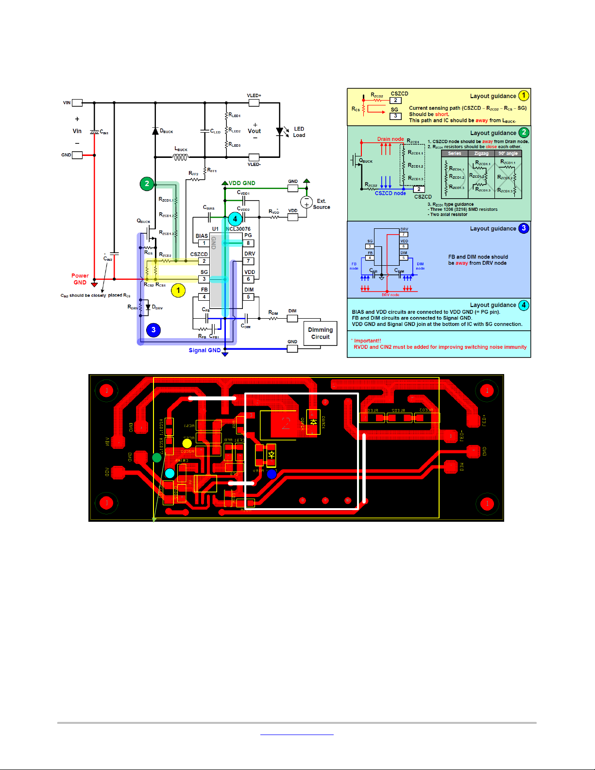
PCB LAYOUT GUIDANCE
Jumper
L
BUCK
3
Jumper
1
2
4
* RZCD1 should be properly selected according to rated voltage.
Figure 16. Layout Guidance
Jumper
www.onsemi.com
12
Page 13
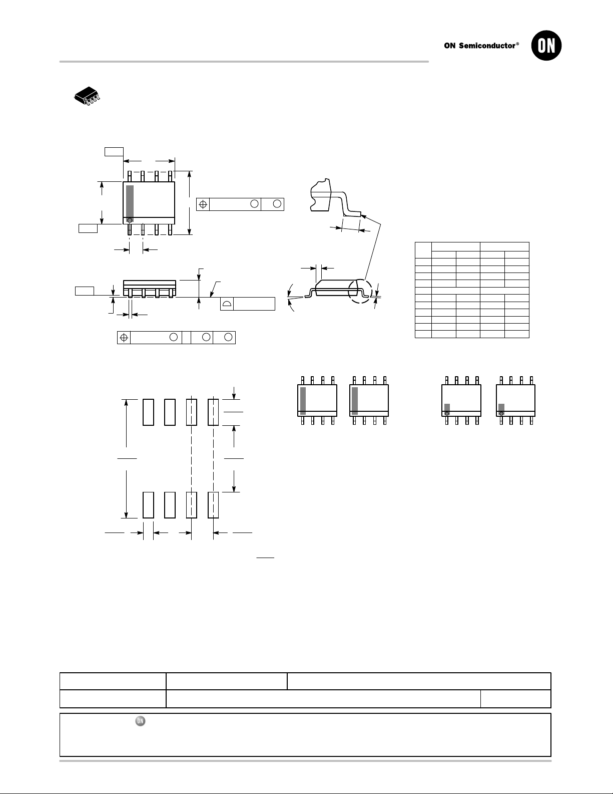
MECHANICAL CASE OUTLINE
PACKAGE DIMENSIONS
8
1
SCALE 1:1
B
−Y−
−Z−
H
−X−
A
58
S
1
4
G
D
0.25 (0.010) Z
M
SOLDERING FOOTPRINT*
7.0
0.275
Y
0.25 (0.010)
C
SXS
SEATING
PLANE
0.10 (0.004)
1.52
0.060
4.0
0.155
CASE 751−07
M
M
Y
N
SOIC−8 NB
ISSUE AK
K
X 45
_
M
J
MARKING DIAGRAM*
8
XXXXX
ALYWX
1
XXXXX = Specific Device Code
A = Assembly Location
L = Wafer Lot
Y = Year
W = Work Week
G = Pb−Free Package
8
XXXXX
ALYWX
G
1
IC
IC
(Pb−Free)
DATE 16 FEB 2011
NOTES:
1. DIMENSIONING AND TOLERANCING PER
ANSI Y14.5M, 1982.
2. CONTROLLING DIMENSION: MILLIMETER.
3. DIMENSION A AND B DO NOT INCLUDE
MOLD PROTRUSION.
4. MAXIMUM MOLD PROTRUSION 0.15 (0.006)
PER SIDE.
5. DIMENSION D DOES NOT INCLUDE DAMBAR
PROTRUSION. ALLOWABLE DAMBAR
PROTRUSION SHALL BE 0.127 (0.005) TOTAL
IN EXCESS OF THE D DIMENSION AT
MAXIMUM MATERIAL CONDITION.
6. 751−01 THRU 751−06 ARE OBSOLETE. NEW
STANDARD IS 751−07.
MILLIMETERS
DIMAMIN MAX MIN MAX
4.80 5.00 0.189 0.197
B 3.80 4.00 0.150 0.157
C 1.35 1.75 0.053 0.069
D 0.33 0.51 0.013 0.020
G 1.27 BSC 0.050 BSC
H 0.10 0.25 0.004 0.010
J 0.19 0.25 0.007 0.010
K 0.40 1.27 0.016 0.050
M 0 8 0 8
____
N 0.25 0.50 0.010 0.020
S 5.80 6.20 0.228 0.244
INCHES
GENERIC
8
XXXXXX
AYWW
1
Discrete
XXXXXX = Specific Device Code
A = Assembly Location
Y = Year
WW = Work Week
G = Pb−Free Package
8
XXXXXX
AYWW
1
Discrete
(Pb−Free)
G
0.6
0.024
1.270
0.050
SCALE 6:1
ǒ
inches
mm
Ǔ
*This information is generic. Please refer to
device data sheet for actual part marking.
Pb−Free indicator, “G” or microdot “G”, may
or may not be present. Some products may
not follow the Generic Marking.
*For additional information on our Pb−Free strategy and soldering
details, please download the ON Semiconductor Soldering and
Mounting Techniques Reference Manual, SOLDERRM/D.
STYLES ON PAGE 2
DOCUMENT NUMBER:
DESCRIPTION:
ON Semiconductor and are trademarks of Semiconductor Components Industries, LLC dba ON Semiconductor or its subsidiaries in the United States and/or other countries.
ON Semiconductor reserves the right to make changes without further notice to any products herein. ON Semiconductor makes no warranty, representation or guarantee regarding
the suitability of its products for any particular purpose, nor does ON Semiconductor assume any liability arising out of the application or use of any product or circuit, and specifically
disclaims any and all liability, including without limitation special, consequential or incidental damages. ON Semiconductor does not convey any license under its patent rights nor the
rights of others.
© Semiconductor Components Industries, LLC, 2019
98ASB42564B
SOIC−8 NB
Electronic versions are uncontrolled except when accessed directly from the Document Repository.
Printed versions are uncontrolled except when stamped “CONTROLLED COPY” in red.
PAGE 1 OF 2
www.onsemi.com
Page 14

STYLE 1:
PIN 1. EMITTER
2. COLLECTOR
3. COLLECTOR
4. EMITTER
5. EMITTER
6. BASE
7. BASE
8. EMITTER
STYLE 5:
PIN 1. DRAIN
2. DRAIN
3. DRAIN
4. DRAIN
5. GATE
6. GATE
7. SOURCE
8. SOURCE
STYLE 9:
PIN 1. EMITTER, COMMON
2. COLLECTOR, DIE #1
3. COLLECTOR, DIE #2
4. EMITTER, COMMON
5. EMITTER, COMMON
6. BASE, DIE #2
7. BASE, DIE #1
8. EMITTER, COMMON
STYLE 13:
PIN 1. N.C.
2. SOURCE
3. SOURCE
4. GATE
5. DRAIN
6. DRAIN
7. DRAIN
8. DRAIN
STYLE 17:
PIN 1. VCC
2. V2OUT
3. V1OUT
4. TXE
5. RXE
6. VEE
7. GND
8. ACC
STYLE 21:
PIN 1. CATHODE 1
2. CATHODE 2
3. CATHODE 3
4. CATHODE 4
5. CATHODE 5
6. COMMON ANODE
7. COMMON ANODE
8. CATHODE 6
STYLE 25:
PIN 1. VIN
2. N/C
3. REXT
4. GND
5. IOUT
6. IOUT
7. IOUT
8. IOUT
STYLE 29:
PIN 1. BASE, DIE #1
2. EMITTER, #1
3. BASE, #2
4. EMITTER, #2
5. COLLECTOR, #2
6. COLLECTOR, #2
7. COLLECTOR, #1
8. COLLECTOR, #1
STYLE 2:
PIN 1. COLLECTOR, DIE, #1
2. COLLECTOR, #1
3. COLLECTOR, #2
4. COLLECTOR, #2
5. BASE, #2
6. EMITTER, #2
7. BASE, #1
8. EMITTER, #1
STYLE 6:
PIN 1. SOURCE
2. DRAIN
3. DRAIN
4. SOURCE
5. SOURCE
6. GATE
7. GATE
8. SOURCE
STYLE 10:
PIN 1. GROUND
2. BIAS 1
3. OUTPUT
4. GROUND
5. GROUND
6. BIAS 2
7. INPUT
8. GROUND
STYLE 14:
PIN 1. N−SOURCE
2. N−GATE
3. P−SOURCE
4. P−GATE
5. P−DRAIN
6. P−DRAIN
7. N−DRAIN
8. N−DRAIN
STYLE 18:
PIN 1. ANODE
2. ANODE
3. SOURCE
4. GATE
5. DRAIN
6. DRAIN
7. CATHODE
8. CATHODE
STYLE 22:
PIN 1. I/O LINE 1
2. COMMON CATHODE/VCC
3. COMMON CATHODE/VCC
4. I/O LINE 3
5. COMMON ANODE/GND
6. I/O LINE 4
7. I/O LINE 5
8. COMMON ANODE/GND
STYLE 26:
PIN 1. GND
2. dv/dt
3. ENABLE
4. ILIMIT
5. SOURCE
6. SOURCE
7. SOURCE
8. VCC
STYLE 30:
PIN 1. DRAIN 1
2. DRAIN 1
3. GATE 2
4. SOURCE 2
5. SOURCE 1/DRAIN 2
6. SOURCE 1/DRAIN 2
7. SOURCE 1/DRAIN 2
8. GATE 1
SOIC−8 NB
CASE 751−07
ISSUE AK
STYLE 3:
STYLE 7:
STYLE 11:
STYLE 15:
STYLE 19:
STYLE 23:
PIN 1. DRAIN, DIE #1
2. DRAIN, #1
3. DRAIN, #2
4. DRAIN, #2
5. GATE, #2
6. SOURCE, #2
7. GATE, #1
8. SOURCE, #1
PIN 1. INPUT
2. EXTERNAL BYPASS
3. THIRD STAGE SOURCE
4. GROUND
5. DRAIN
6. GATE 3
7. SECOND STAGE Vd
8. FIRST STAGE Vd
PIN 1. SOURCE 1
2. GATE 1
3. SOURCE 2
4. GATE 2
5. DRAIN 2
6. DRAIN 2
7. DRAIN 1
8. DRAIN 1
PIN 1. ANODE 1
2. ANODE 1
3. ANODE 1
4. ANODE 1
5. CATHODE, COMMON
6. CATHODE, COMMON
7. CATHODE, COMMON
8. CATHODE, COMMON
PIN 1. SOURCE 1
2. GATE 1
3. SOURCE 2
4. GATE 2
5. DRAIN 2
6. MIRROR 2
7. DRAIN 1
8. MIRROR 1
PIN 1. LINE 1 IN
2. COMMON ANODE/GND
3. COMMON ANODE/GND
4. LINE 2 IN
5. LINE 2 OUT
6. COMMON ANODE/GND
7. COMMON ANODE/GND
8. LINE 1 OUT
STYLE 27:
PIN 1. ILIMIT
2. OVLO
3. UVLO
4. INPUT+
5. SOURCE
6. SOURCE
7. SOURCE
8. DRAIN
DATE 16 FEB 2011
STYLE 4:
PIN 1. ANODE
2. ANODE
3. ANODE
4. ANODE
5. ANODE
6. ANODE
7. ANODE
8. COMMON CATHODE
STYLE 8:
PIN 1. COLLECTOR, DIE #1
2. BASE, #1
3. BASE, #2
4. COLLECTOR, #2
5. COLLECTOR, #2
6. EMITTER, #2
7. EMITTER, #1
8. COLLECTOR, #1
STYLE 12:
PIN 1. SOURCE
2. SOURCE
3. SOURCE
4. GATE
5. DRAIN
6. DRAIN
7. DRAIN
8. DRAIN
STYLE 16:
PIN 1. EMITTER, DIE #1
2. BASE, DIE #1
3. EMITTER, DIE #2
4. BASE, DIE #2
5. COLLECTOR, DIE #2
6. COLLECTOR, DIE #2
7. COLLECTOR, DIE #1
8. COLLECTOR, DIE #1
STYLE 20:
PIN 1. SOURCE (N)
2. GATE (N)
3. SOURCE (P)
4. GATE (P)
5. DRAIN
6. DRAIN
7. DRAIN
8. DRAIN
STYLE 24:
PIN 1. BASE
2. EMITTER
3. COLLECTOR/ANODE
4. COLLECTOR/ANODE
5. CATHODE
6. CATHODE
7. COLLECTOR/ANODE
8. COLLECTOR/ANODE
STYLE 28:
PIN 1. SW_TO_GND
2. DASIC_OFF
3. DASIC_SW_DET
4. GND
5. V_MON
6. VBULK
7. VBULK
8. VIN
DOCUMENT NUMBER:
DESCRIPTION:
ON Semiconductor and are trademarks of Semiconductor Components Industries, LLC dba ON Semiconductor or its subsidiaries in the United States and/or other countries.
ON Semiconductor reserves the right to make changes without further notice to any products herein. ON Semiconductor makes no warranty, representation or guarantee regarding
the suitability of its products for any particular purpose, nor does ON Semiconductor assume any liability arising out of the application or use of any product or circuit, and specifically
disclaims any and all liability, including without limitation special, consequential or incidental damages. ON Semiconductor does not convey any license under its patent rights nor the
rights of others.
© Semiconductor Components Industries, LLC, 2019
98ASB42564B
SOIC−8 NB
Electronic versions are uncontrolled except when accessed directly from the Document Repository.
Printed versions are uncontrolled except when stamped “CONTROLLED COPY” in red.
PAGE 2 OF 2
www.onsemi.com
Page 15

ON Semiconductor and are trademarks of Semiconductor Components Industries, LLC dba ON Semiconductor or its subsidiaries in the United States and/or other countries.
ON Semiconductor owns the rights to a number of patents, trademarks, copyrights, trade secrets, and other intellectual property. A listing of ON Semiconductor ’s product/patent
coverage may be accessed at www.onsemi.com/site/pdf/Patent−Marking.pdf
ON Semiconductor makes no warranty, representation or guarantee regarding the suitability of its products for any particular purpose, nor does ON Semiconductor assume any liability
arising out of the application or use of any product or circuit, and specifically disclaims any and all liability, including without limitation special, consequential or incidental damages.
Buyer is responsible for its products and applications using ON Semiconductor products, including compliance with all laws, regulations and safety requirements or standards,
regardless of any support or applications information provided by ON Semiconductor. “Typical” parameters which may be provided in ON Semiconductor data sheets and/or
specifications can and do vary in different applications and actual performance may vary over time. All operating parameters, including “Typicals” must be validated for each customer
application by customer’s technical experts. ON Semiconductor does not convey any license under its patent rights nor the rights of others. ON Semiconductor products are not
designed, intended, or authorized for use as a critical component in life support systems or any FDA Class 3 medical devices or medical devices with a same or similar classification
in a foreign jurisdiction or any devices intended for implantation in the human body. Should Buyer purchase or use ON Semiconductor products for any such unintended or unauthorized
application, Buyer shall indemnify and hold ON Semiconductor and its officers, employees, subsidiaries, affiliates, and distributors harmless against all claims, costs, damages, and
expenses, and reasonable attorney fees arising out of, directly or indirectly, any claim of personal injury or death associated with such unintended or unauthorized use, even if such
claim alleges that ON Semiconductor was negligent regarding the design or manufacture of the part. ON Semiconductor is an Equal Opportunity/Affirmative Action Employer. This
literature is subject to all applicable copyright laws and is not for resale in any manner.
. ON Semiconductor reserves the right to make changes without further notice to any products herein.
PUBLICATION ORDERING INFORMATION
LITERATURE FULFILLMENT:
Email Requests to: [email protected]
ON Semiconductor Website: www.onsemi.com
TECHNICAL SUPPORT
North American Technical Support:
Voice Mail: 1 800−282−9855 Toll Free USA/Canada
Phone: 011 421 33 790 2910
Europe, Middle East and Africa Technical Support:
Phone: 00421 33 790 2910
For additional information, please contact your local Sales Representative
◊
www.onsemi.com
1
 Loading...