

Page 1
NC7SP38 — TinyLogic
September 2008
NC7SP38
TinyLogic
®
ULP 2-Input NAND Gate (Open Drain Output)
Features
■
0.9V to 3.6V V
■
3.6V overvoltage tolerant I/O’s at V
3.6V
■
t
:
PD
– 3.0ns typ. for 3.0V to 3.6V V
– 4.0ns typ. for 2.3V to 2.7V V
– 5.0ns typ. for 1.65V to 1.95V V
– 6.0ns typ. for 1.40V to 1.60V V
– 9.0ns typ. for 1.10V to 1.30V V
– 24.0ns typ. for 0.90V V
■
Power-off high impedance inputs and outputs
■
Static drive (I
– ±2.6mA @ 3.00V V
– ±2.1mA @ 2.30V V
– ±1.5mA @ 1.65V V
– ±1.0mA @ 1.40V V
– ±0.5mA @ 1.10V V
– ±20µA @ 0.9V V
Uses patented Quiet Series™ noise/EMI reduction
■
circuitry
■
Ultra small MicroPak™ package
Ultra low dynamic power
■
supply operation
CC
/I
):
OH
OL
CC
CC
CC
CC
CC
CC
CC
CC
CC
CC
CC
CC
CC
from 0.9V to
General Description
The NC7SP38 is a single 2-Input NAND Gate with
open drain output stage from Fairchild’s Ultra Low
Power (ULP) Series of TinyLogic
where battery life is critical, this product is designed for
ultra low power consumption within the V
range of 0.9V to 3.6V V
CC
The internal circuit is composed of a minimum of inverter
stages including the output buffer, to enable ultra low
static and dynamic power.
The NC7SP38, for lower drive requirements, is uniquely
designed for optimized power and speed, and is fabricated with an advanced CMOS technology to achieve
best in class speed operation while maintaining
extremely low CMOS power dissipation.
. Ideal for applications
operating
CC
.
®
ULP 2-Input NAND Gate (Open Drain Output)
Ordering Information
Order
Number
NC7SP38P5X MAA05A P38 5-Lead SC70, EIAJ SC-88a,
NC7SP38L6X MAC06A K7
All packages are lead free per JEDEC: J-STD-020B standard.
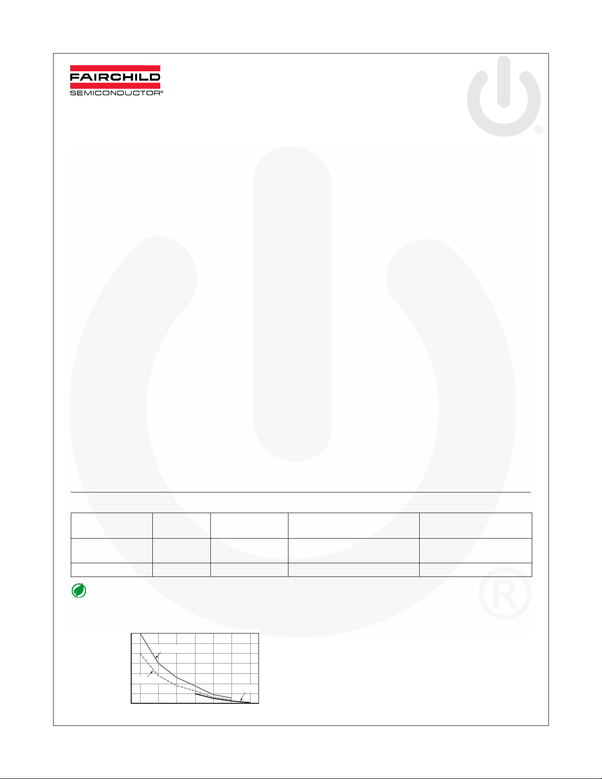
Battery Life vs. V
700
600
Battery Life
(Days)
©2004 Fairchild Semiconductor Corporation www.fairchildsemi.com
NC7SP38 Rev. 1.0.0
500
400
300
200
100
ULP-A (SV)
0
ULP (SP)
0.9 1.2
Package
Number
Supply Voltage
CC
1.5 1.8 2.5 3.3 5.0
Supply Voltage
V
CC
Package Code
Top Mark Package Description Supplied As
UHS (SZ)
3k Units on Tape and Reel
1.25mm Wide
6-Lead MicroPak, 1.0mm Wide 5k Units on Tape and Reel
TinyLogic ULP and ULP-A with up to 50% less power consumption can
extend your battery life significantly.
Battery Life = (V
Where, P
Assumes ideal 3.6V Lithium Ion battery with current rating of 900mAH
and derated 90% and device frequency at 10MHz, with CL = 15pF load.
device
battery
= (I
x I
battery
x VCC) + (C
CC
x 0.9) / (P
+ CL) x V
PD
device
) / 24hrs/day
2
x f
CC
Page 2
k
Y =
H =
NC7SP38 — TinyLogic
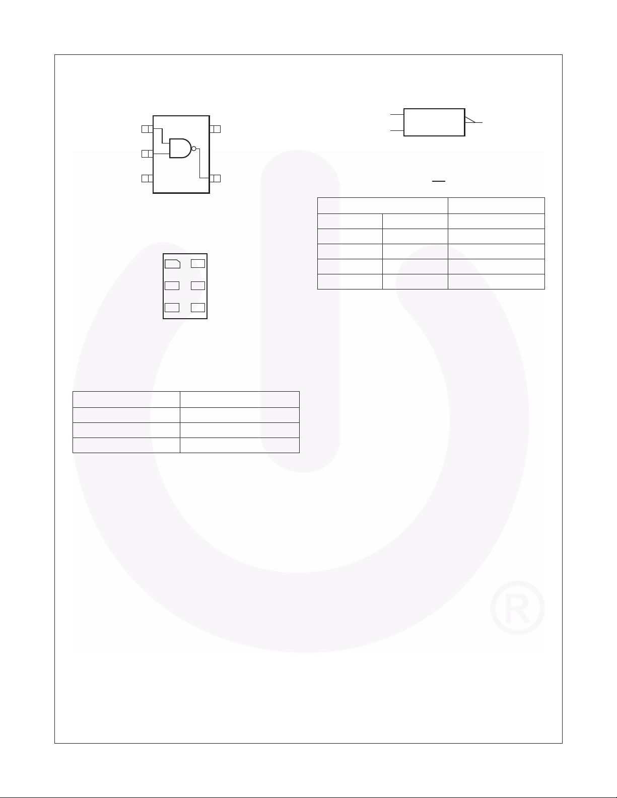
Connection Diagrams
Pin Assignment for SC70
1 5
A
2
B
3 4
GND
(Top View)
Pad Assignments for MicroPa
1
A
2
B
3
GND
(Top Through View)
Logic Symbol
IEEE/IEC
A
V
CC
B
&
Y
Function Table
Y
AB
Inputs Output
AB Y
LL *H
LH *H
6
V
CC
5
NC
4
Y
HL *H
HH L
HIGH Logic Level
L = LOW Logic Level
*H = HIGH Impedance Output State (Open Drain)
®
ULP 2-Input NAND Gate (Open Drain Output)
Pin Description
Pin Names Description
A, B Input
Y Output
NC No Connect
©2004 Fairchild Semiconductor Corporation www.fairchildsemi.com
NC7SP38 Rev. 1.0.0 2
Page 3

=
<
<
>
=
=
=
=
=
=
=
NC7SP38 — TinyLogic
Absolute Maximum Ratings
Stresses exceeding the absolute maximum ratings may damage the device. The device may not function or be
operable above the recommended operating conditions and stressing the parts to these levels is not recommended.
In addition, extended exposure to stresses above the recommended operating conditions may affect device reliability.
The absolute maximum ratings are stress ratings only.
Symbol Parameter Rating
V
CC
V
IN
V
OUT
I
IK
I
OK
I
/
I
OH
OL
I
or Ground DC V
CC
T
STG
T
J
T
L
P
D
Supply Voltage –0.5V to +4.6V
DC Input Voltage –0.5V to +4.6V
DC Output Voltage
HIGH or LOW State
V
0V
CC
DC Input Diode Current @ V
(1)
–0.5V to V
–0.5V to +4.6V
0V –50mA
IN
CC
+0.5V
DC Output Diode Current
V
V
OUT
OUT
0V
V
CC
–50mA
+50mA
DC Output Source/Sink Current ±50mA
or Ground Current per Supply Pin ±50mA
CC
Storage Temperature Range –65°C to +150°C
Junction Temperature Under Bias 150°C
Junction Lead Temperature (Soldering, 10 seconds) 260°C
Power Dissipation @ +85°C
SC70-5
Micropak-6
150mW
130mW
®
ULP 2-Input NAND Gate (Open Drain Output)
∆
∆ V
=
Recommended Operating Conditions
(2)
The Recommended Operating Conditions table defines the conditions for actual device operation. Recommended
operating conditions are specified to ensure optimal performance to the datasheet specifications. Fairchild does not
recommend exceeding them or designing to absolute maximum ratings.
Symbol Parameter Rating
I
V
OH
V
V
OUT
T
t
θ
CC
/
JA
IN
/
A
Supply Voltage 0.9V to 3.6V
Input Voltage 0V to 3.6V
Output Voltage
HIGH or LOW State
V
0V
CC
I
Output Current in I
OL
V
3.0V to 3.6V
CC
V
2.3V to 2.7V
CC
V
1.65V to 1.95V
CC
V
1.40V to 1.60V
CC
V
1.10V to 1.30V
CC
V
0.9V
CC
OH
/
I
OL
Free Air Operating Temperature –40°C to +85°C
Minimum Input Edge Rate @ V
0.8V to 2.0V, V
IN
= 3.0V 10ns/V
CC
Thermal Resistance
SC70-5
Micropak-6
0V to V
CC
0V to 3.6V
±2.6mA
±2.1mA
±1.5mA
±1mA
±0.5mA
±20µA
425°C/W
500°C/W
Notes:
1. I
Absolute Maximum Rating must be observed.
O
2. Unused inputs must be held HIGH or LOW. They may not float.
©2004 Fairchild Semiconductor Corporation www.fairchildsemi.com
NC7SP38 Rev. 1.0.0 3
Page 4
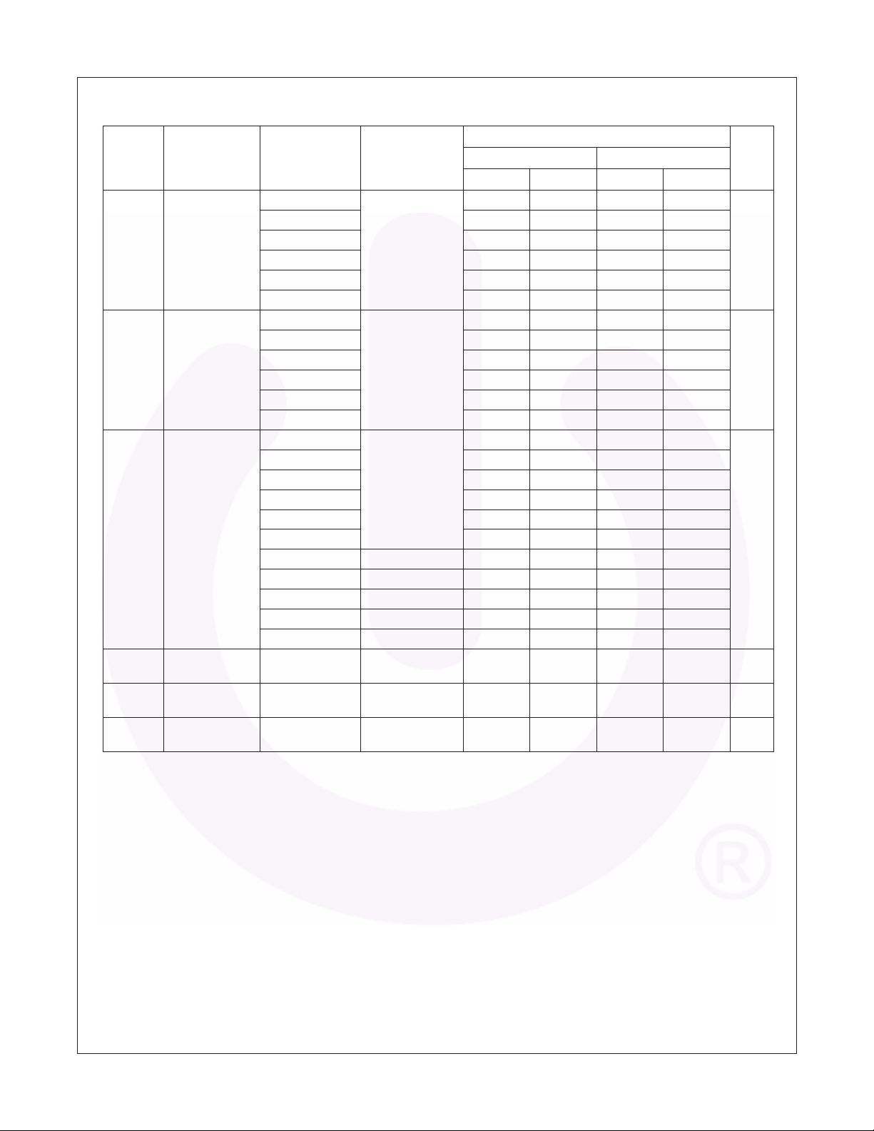
DC Electrical Characteristics
Symbol Parameter V
V
V
I
I
V
OL
I
IN
OFF
CC
IH
IL
HIGH Level
Input Voltage
LOW Level
Input Voltage
LOW Level
Output Voltage
Input Leakage
Current
Power Off
Leakage Current
Quiescent
Supply Current
1.10 ≤ VCC ≤ 1.30 0.65 x V
1.40 ≤ VCC ≤ 1.60 0.65 x V
1.65 ≤ VCC ≤ 1.95 0.65 x V
2.30 ≤ VCC ≤ 2.70 1.6 1.6
3.00 ≤ VCC ≤ 3.60 2.1 2.1
1.10 ≤ VCC ≤ 1.30 0.35 x V
1.40 ≤ VCC ≤ 1.60 0.35 x V
1.65 ≤ VCC ≤ 1.95 0.35 x V
2.30 ≤ VCC ≤ 2.70 0.7 0.7
3.00 ≤ VCC ≤ 3.60 0.9 0.9
1.10 ≤ VCC ≤ 1.30 0.1 0.1
1.40 ≤ VCC ≤ 1.60 0.1 0.1
1.65 ≤ VCC ≤ 1.95 0.1 0.1
2.30 ≤ VCC ≤ 2.70 0.1 0.1
3.00 ≤ VCC ≤ 3.60 0.1 0.1
1.10 ≤ VCC ≤ 1.30 IOL = 0.5mA 0.30 x V
1.40 ≤ VCC ≤ 1.60 IOL = 1mA 0.31 0.37
1.65 ≤ VCC ≤ 1.95 IOL = 1.5mA 0.31 0.35
2.30 ≤ VCC ≤ 2.70 IOL = 2.1mA 0.31 0.33
3.00 ≤ VCC ≤ 3.60 IOL = 2.6mA 0.31 0.33
(V) Conditions
CC
0.90 0.65 x V
0.90 0.35 x V
0.90 IOL = 20µA 0.1 0.1 V
0.90 to 3.60 0 ≤ VI ≤ 3.6V ±0.1 ±0.5 µA
00 ≤ (VI, VO) ≤ 3.6V 0.5 0.5 µA
0.90 to 3.60 VI = VCC or GND 0.9 0.9 µA
=
T
A
+25°C –40°C to +85°C
Min. Max. Min. Max.
CC
CC
CC
CC
CC
0.65 x V
0.65 x V
0.65 x V
0.65 x V
CC
CC
CC
CC
0.35 x V
0.35 x V
0.35 x V
0.35 x V
0.30 x V
CC
CC
CC
CC
CC
CC
CC
CC
CC
Units
V
V
NC7SP38 — TinyLogic
®
ULP 2-Input NAND Gate (Open Drain Output)
©2004 Fairchild Semiconductor Corporation www.fairchildsemi.com
NC7SP38 Rev. 1.0.0 4
Page 5
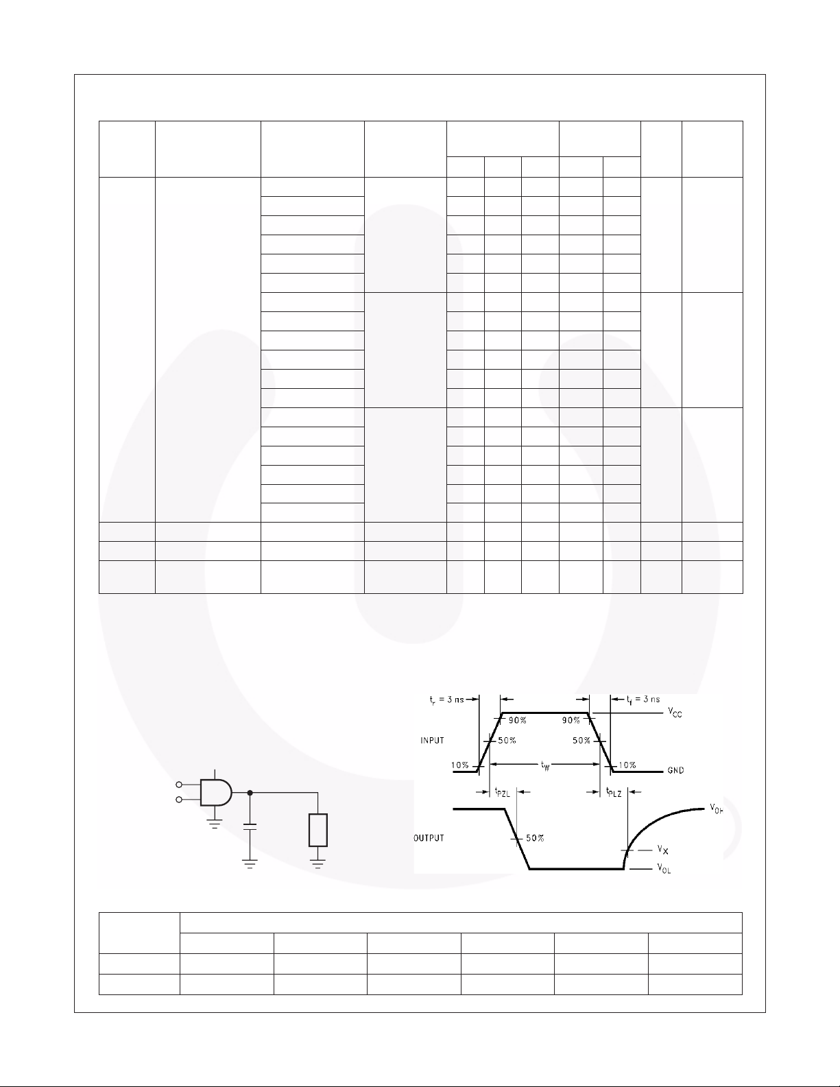
AC Electrical Characteristics
Symbol Parameter V
t
, t
PZL
C
C
Propagation Delay 0.9 CL = 10pF,
PLZ
C
Input Capacitance 0 2.0 pF
IN
Output Capacitance 0 4.0 pF
OUT
Power Dissipation
PD
Capacitance
CC
1.10 ≤ VCC ≤ 1.30 4.0 9 18.7 3.5 30.9
1.40 ≤ VCC ≤ 1.60 2.0 6 12.4 1.5 13.9
1.65 ≤ VCC ≤ 1.95 1.5 5 9.6 1.0 12.1
2.30 ≤ VCC ≤ 2.70 1.0 4 9.0 0.8 10.0
3.00 ≤ VCC ≤ 3.60 1.0 3 8.7 0.5 9.0
0.90 CL = 15pF,
1.10 ≤ VCC ≤ 1.30 5.0 10 20.0 4.5 33.9
1.40 ≤ VCC ≤ 1.60 3.0 7 13.3 2.5 16.0
1.65 ≤ VCC ≤ 1.95 2.0 5 10.3 2.0 12.6
2.30 ≤ VCC ≤ 2.70 1.5 4 9.4 1.0 10.2
3.00 ≤ VCC ≤ 3.60 1.0 3 9.1 0.5 9.7
0.90 CL = 30pF,
1.10 ≤ VCC ≤ 1.30 6.0 12 24.0 5.0 43.0
1.40 ≤ VCC ≤ 1.60 4.0 8 16.0 3.0 18.0
1.65 ≤ VCC ≤ 1.95 2.0 6 12.0 2.0 14.0
2.30 ≤ VCC ≤ 2.70 1.0 5 11.0 1.0 12.0
3.00 ≤ VCC ≤ 3.60 0.8 4 10.0 0.5 11.0
0.9 to 3.60 VI = 0V or VCC,
(V) Conditions
RU = 5,000Ω,
RD = 5,000Ω
RU = 5,000Ω,
RD = 5,000Ω
RU = 5,000Ω,
RD = 5,000Ω
f = 10MHz
= –40°C
T
T
= +25°C
A
24 ns Figure 1
27 ns Figure 1
34 ns Figure 1
6pF
A
to +85°C
Units
Figure
NumberMin. Typ. Max. Min. Max.
Figure 2
Figure 2
Figure 2
NC7SP38 — TinyLogic
®
ULP 2-Input NAND Gate (Open Drain Output)
AC Loading and Waveforms
V
CC
TEST
SIGNAL
Symbol
V
mi
V
x
©2004 Fairchild Semiconductor Corporation www.fairchildsemi.com
NC7SP38 Rev. 1.0.0 5
DUT
CL pF RL Ω
Figure 1. AC Test Circuit Figure 2. AC Waveforms
V
CC
3.3V ± 0.3V 2.5V ± 0.2V 1.8V ± 0.15V 1.5V ± 0.1V 1.2V ± 0.1V 0.9V
1.5V V
/ 2V
CC
/ 2V
CC
/ 2V
CC
/ 2V
CC
VOL + 0.3V VOL + 0.15V VOL + 0.15V VOL + 0.1V VOL + 0.1V VOL + 0.1V
CC
/ 2
Page 6
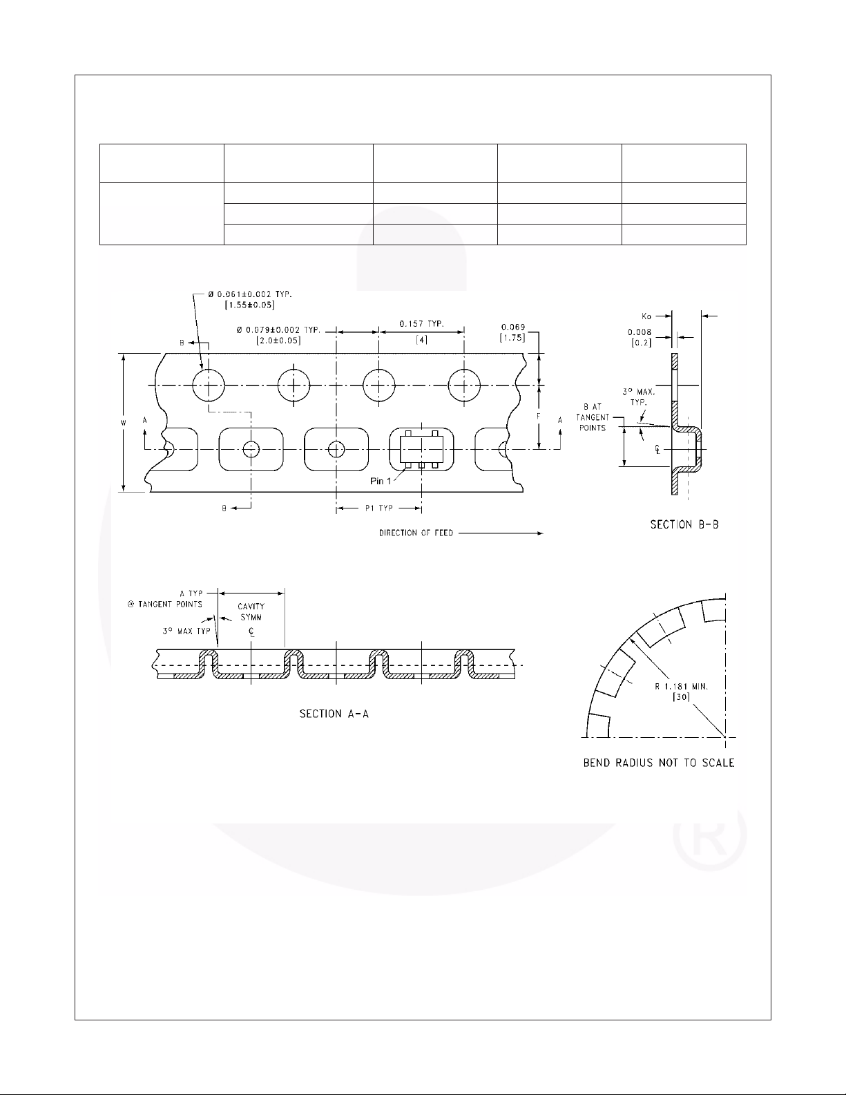
Tape and Reel Specification
Tape Format for SC70
Package
Designator
P5X Leader (Start End) 125 (typ.) Empty Sealed
Tape Dimension inches (millimeters)
Tape
Section
Carrier 3000 Filled Sealed
Tr ailer (Hub End) 75 (typ.) Empty Sealed
Number
Cavities
Cavity
Status
Cover Tape
Status
NC7SP38 — TinyLogic
®
ULP 2-Input NAND Gate (Open Drain Output)
©2004 Fairchild Semiconductor Corporation www.fairchildsemi.com
NC7SP38 Rev. 1.0.0 6
Page 7
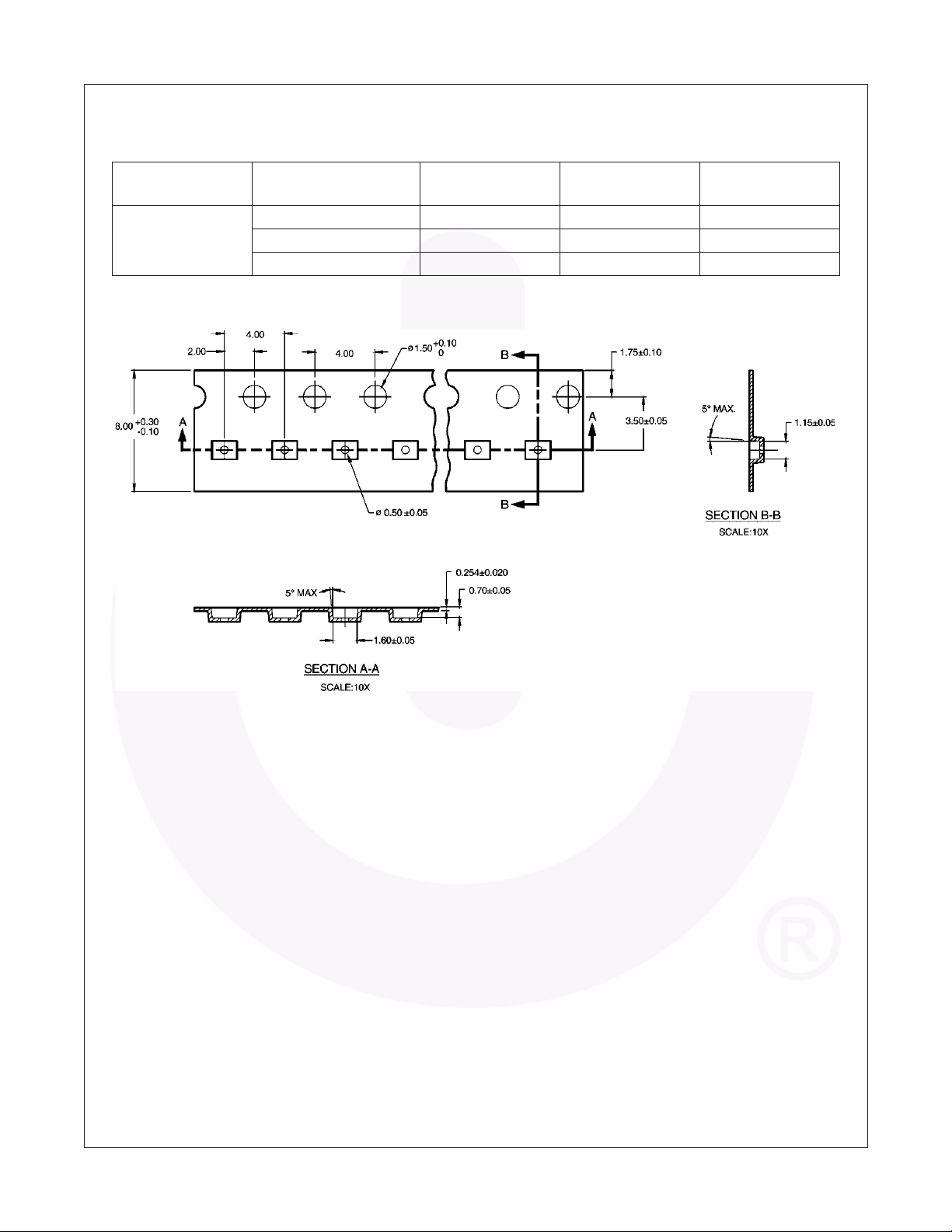
Tape and Reel Specification (Continued)
Tape Format for MicroPak
Package
Designator
L6X Leader (Start End) 125 (typ.) Empty Sealed
Tape Dimension millimeters
Tape
Section
Carrier 5000 Filled Sealed
Tr ailer (Hub End) 75 (typ.) Empty Sealed
Number
Cavities
Cavity
Status
Cover Tape
Status
NC7SP38 — TinyLogic
®
ULP 2-Input NAND Gate (Open Drain Output)
©2004 Fairchild Semiconductor Corporation www.fairchildsemi.com
NC7SP38 Rev. 1.0.0 7
Page 8
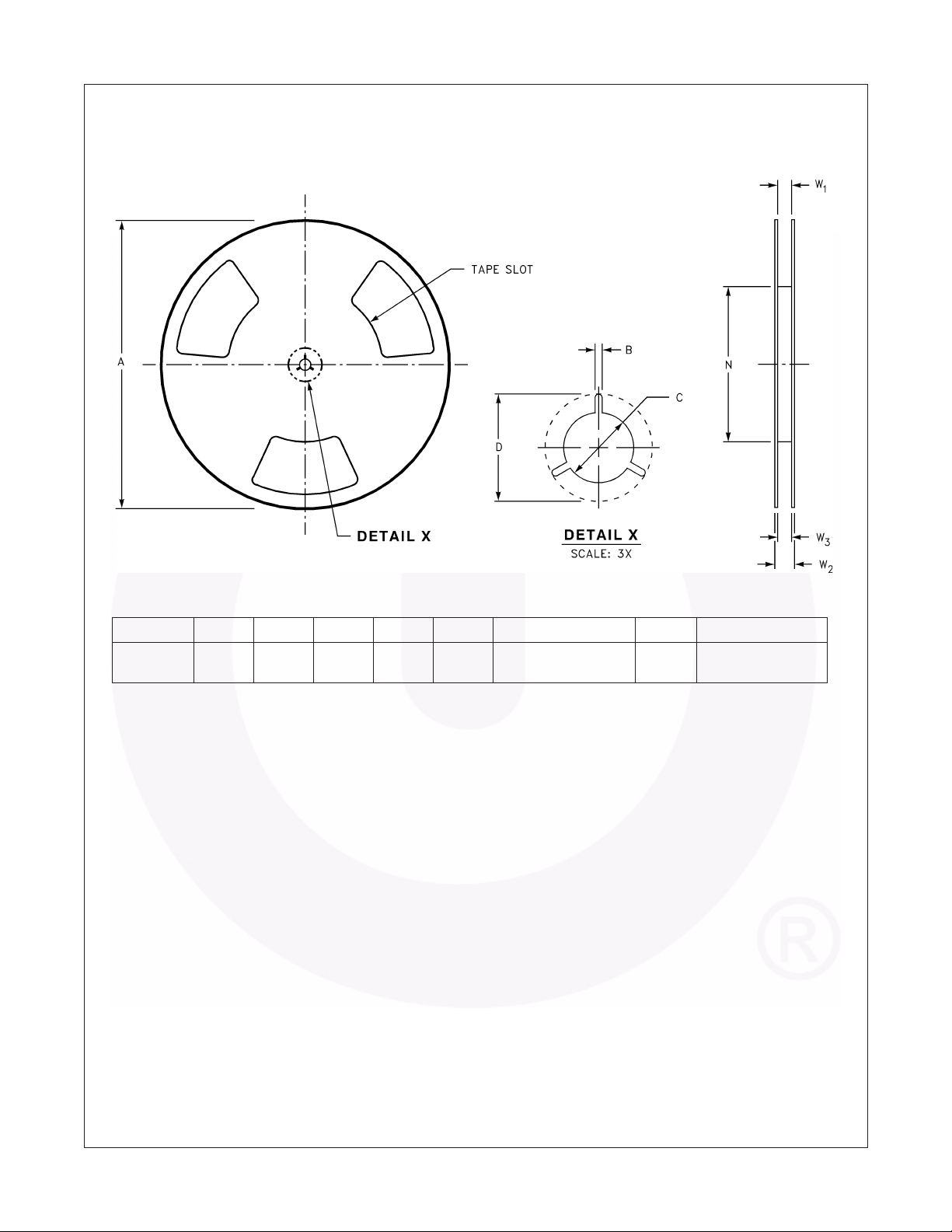
Tape and Reel Specification (Continued)
Reel Dimension for MicroPak inches (millimeters)
NC7SP38 — TinyLogic
®
ULP 2-Input NAND Gate (Open Drain Output)
Tape Size ABCDN W
8mm 7.0
(177.8)
0.059
(1.50)
0.512
(13.00)
0.795
(20.20)
2.165
(55.00)
0.331 +0.059/–0.000
(8.40 +1.50/–0.00)
1
W
2
0.567
(14.40)
W
3
W1 +0.078/–0.039
(W1 +2.00/–1.00)
©2004 Fairchild Semiconductor Corporation www.fairchildsemi.com
NC7SP38 Rev. 1.0.0 8
Page 9
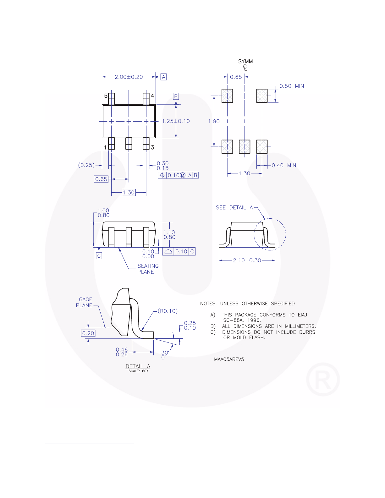
Physical Dimensions
RECOMMENED
LAND PATTERN
NC7SP38 — TinyLogic
®
ULP 2-Input NAND Gate (Open Drain Output)
Figure 3. 5-Lead SC70, EIAJ SC-88a, 1.25mm Wide
Package drawings are provided as a service to customers considering Fairchild components. Drawings may change in any manner
without notice. Please note the revision and/or date on the drawing and contact a Fairchild Semiconductor representative to verify or
obtain the most recent revision. Package specifications do not expand the terms of Fairchild’s worldwide terms and conditions,
specifically the warranty therein, which covers Fairchild products.
Always visit Fairchild Semiconductor’s online packaging area for the most recent package drawings:
http://www.fairchildsemi.com/packaging/
©2004 Fairchild Semiconductor Corporation www.fairchildsemi.com
NC7SP38 Rev. 1.0.0 9
Page 10
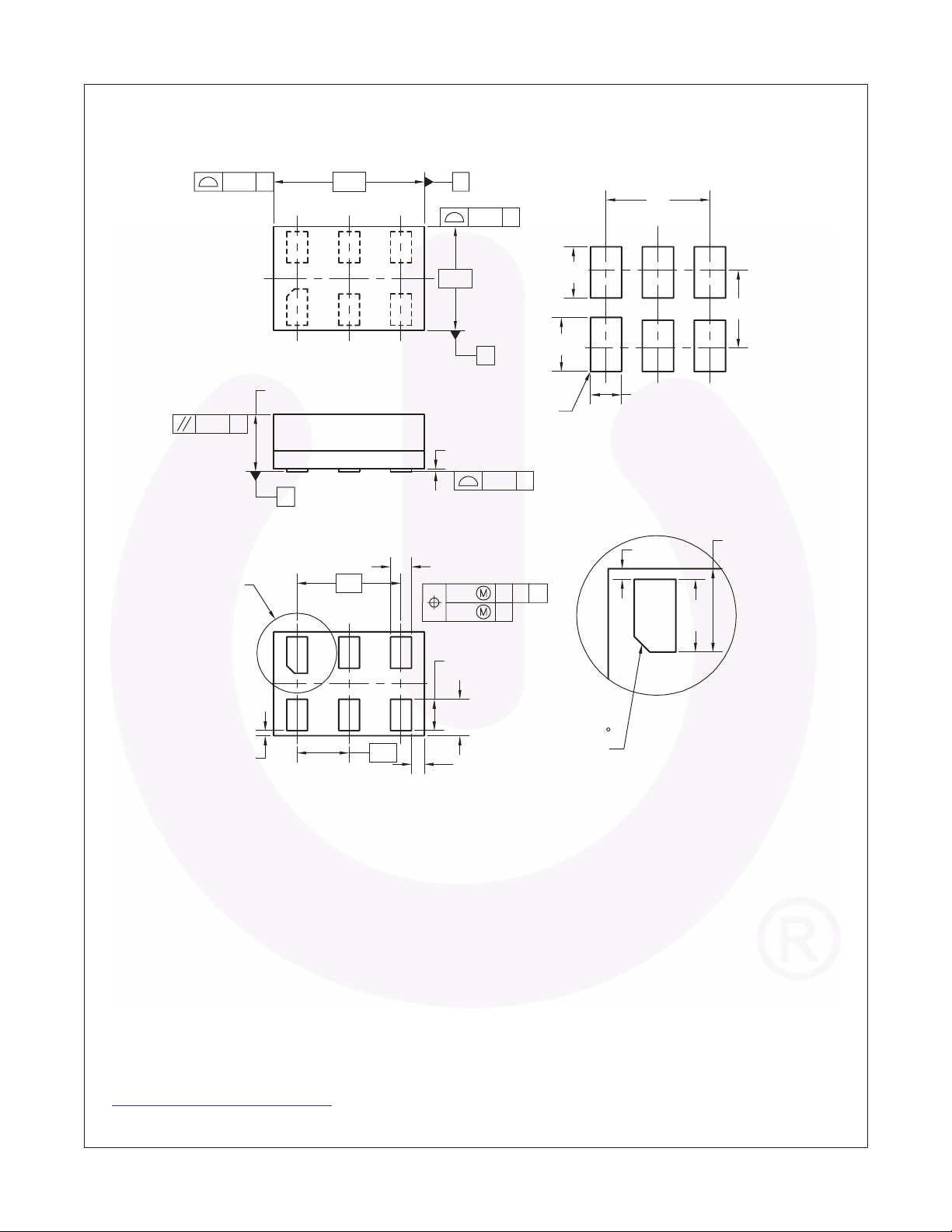
Physical Dimensions (Continued)
2X
1.45
2X
NC7SP38 — TinyLogic
B0.05 C
(1)
0.05 C
0.05
DETAIL A
(0.05)
6X
C
0.55 MAX.
C
BOTTOM VIEW
TOP VIEW
SIDE VIEW
1.0
0.5
1.00
A
0.05
0.00
0.05 C
0.25
6X
0.15
0.10 C B A
0.05 C
0.35
5X
0.25
0.40
5X
0.30
(0.13)
4X
(0.49)
5X
(0.52)
1X
PIN 1
0.075 X 45
CHAMFER
(0.30)
6X
RECOMMENED
LAND PATTERN
0.10
6X
0.00
0.40
0.30
DETAIL A
PIN 1 TERMINAL
(0.75)
0.45
0.35
®
ULP 2-Input NAND Gate (Open Drain Output)
Notes:
1. CONFORMS TO JEDEC STANDARD M0-252 VARIATION UAAD
2. DIMENSIONS ARE IN MILLIMETERS
3. DRAWING CONFORMS TO ASME Y14.5M-1994
MAC06AREVC
Figure 4. 6-Lead MicroPak, 1.0mm Wide
Package drawings are provided as a service to customers considering Fairchild components. Drawings may change in any manner
without notice. Please note the revision and/or date on the drawing and contact a Fairchild Semiconductor representative to verify or
obtain the most recent revision. Package specifications do not expand the terms of Fairchild’s worldwide terms and conditions,
specifically the warranty therein, which covers Fairchild products.
Always visit Fairchild Semiconductor’s online packaging area for the most recent package drawings:
http://www.fairchildsemi.com/packaging/
©2004 Fairchild Semiconductor Corporation www.fairchildsemi.com
NC7SP38 Rev. 1.0.0 10
Page 11
TRADEMARKS
The following includes registered and unregistered trademarks and service marks, owned by Fairchild Semiconductor and/or its global subsidiaries,andis not
intended to be an exhaustive list of all such trademarks.
Build it Now™
CorePLUS™
CorePOWER™
CROSSVOLT™
CTL™
Current Transfer Logic™
EcoSPARK
®
EfficentMax™
EZSWITCH™ *
™
®
®
Fairchild
Fairchild Semiconductor
FACT Quiet Series™
®
FACT
®
FAST
FastvCore™
FlashWriter
®*
®
FPS™
*EZSWITCH™ and FlashWriter
F-PFS™
®
FRFET
Global Power Resource
Green FPS™
Green FPS™ e-Series™
GTO™
SM
PowerTrench
Programmable Active Droop™
QFET
QS™
Quiet Series™
RapidConfigure™
IntelliMAX™
ISOPLANAR™
MegaBuck™
MICROCOUPLER™
MicroFET™
MicroPak™
MillerDrive™
MotionMax™
Motion-SPM™
OPTOLOGIC
OPTOPLANAR
®
®
®
PDP SPM™
Saving our world, 1mW/W/kW at a time™
SmartMax™
SMART START™
SPM
STEALTH™
SuperFET™
SuperSOT™-3
SuperSOT™-6
SuperSOT™-8
SupreMOS™
SyncFET™
Power-SPM™
®
are trademarks of System General Corporation, used under license by Fairchild Semiconductor.
®
®
ThePower Franchise
TinyBoost™
TinyBuck™
®
TinyLogic
™
TINYOPTO™
TinyPower™
TinyPWM™
TinyWire™
®
µSerDes™
®
UHC
Ultra FRFET™
UniFET™
VCX™
VisualMax™
®
NC7SP38 — TinyLogic
®
®
ULP 2-Input NAND Gate (Open Drain Output)
DISCLAIMER
FAIRCHILD SEMICONDUCTOR RESERVES THE RIGHT TO MAKE CHANGES WITHOUT FURTHER NOTICE TO ANY PRODUCTS HEREIN TO IMPROVE
RELIABILITY, FUNCTION, OR DESIGN. FAIRCHILD DOES NOT ASSUME ANY LIABILITY ARISING OUT OF THE APPLICATION OR USE OF ANY PRODUCT OR
CIRCUIT DESCRIBED HEREIN; NEITHER DOES IT CONVEY ANY LICENSE UNDER ITS PATENT RIGHTS, NOR THE RIGHTS OF OTHERS. THESE
SPECIFICATIONS DO NOT EXPAND THE TERMS OF FAIRCHILD’S WORLDWIDE TERMS AND CONDITIONS, SPECIFICALLY THE WARRANTY THEREIN,
WHICH COVERS THESE PRODUCTS.
LIFE SUPPORT POLICY
FAIRCHILD’S PRODUCTS ARE NOT AUTHORIZED FOR USE AS CRITICAL COMPONENTS IN LIFE SUPPORT DEVICES OR SYSTEMS WITHOUT THE
EXPRESS WRITTEN APPROVAL OF FAIRCHILD SEMICONDUCTOR CORPORATION.
As used herein:
1. Life support devices or systems are devices or systems which, (a) are
intended for surgical implant into the body or (b) support or sustain life,
and (c) whose failure to perform when properly used in accordance
with instructions for use provided in the labeling, can be reasonably
2. A critical component in any component of a life support, device, or
system whose failure to perform can be reasonably expected to
cause the failure of the life support device or system, or to affect its
safety or effectiveness.
expected to result in a significant injury of the user.
ANTI-COUNTERFEITING POLICY
Fairchild Semiconductor Corporation's Anti-Counterfeiting Policy. Fairchild's Anti-Counterfeiting Policy is also stated on our external website, www.fairchildsemi.com,
under Sales Support.
Counterfeiting of semiconductor parts is a growing problem in the industry. All manufacturers of semiconductor products are experiencing counterfeiting of their parts.
Customers who inadvertently purchase counterfeit parts experience many problems such as loss of brand reputation, substandard performance, failedapplications,
and increased cost of production and manufacturing delays. Fairchild is taking strong measures to protect ourselves and our customers from the proliferation of
counterfeit parts. Fairchild strongly encourages customers to purchase Fairchild parts either directly from Fairchild or from Authorized Fairchild Distributors who are
listed by country on our web page cited above. Products customers buy either from Fairchild directly or from Authorized Fairchild Distributors are genuine parts, have
full traceability, meet Fairchild's quality standards for handling and storage and provide access to Fairchild's full range of up-to-date technicalandproduct information.
Fairchild and our Authorized Distributors will stand behind all warranties and will appropriately address any warranty issues that may arise. Fairchild will not provide
any warranty coverage or other assistance for parts bought from Unauthorized Sources. Fairchild is committed to combat this global problem and encourage our
customers to do their part in stopping this practice by buying direct or from authorized distributors.
PRODUCT STATUS DEFINITIONS
Definition of Terms
Datasheet Identification P roduct Status Definition
Advance Information Formative / In Design
Preliminary
No Identification Needed Ful
First Production
lProduction
Obsolete Not In Production
Datasheet contains the design specifications for product development. Specifications may change in
any manner without notice.
Datasheet contains preliminary data; supplementary data will be published at a later date. Fairchild
Semiconductor reserves the right to make changes at any time without notice to improve design.
Datasheet contains final specifications. Fairchild Semiconductor reserves the right to make changes
at any time without notice to improve the design.
Datasheet contains specifications on a product that is discontinued by Fairchild Semiconductor. The
datasheet is for reference information only.
Rev. I36
©2004 Fairchild Semiconductor Corporation www.fairchildsemi.com
NC7SP38 Rev. 1.0.0 11
 Loading...