

Page 1
NB670
The Future of Analog IC Technology
DESCRIPTION
The NB670 is a fully integrated high frequency
synchronous rectified step-down switch mode
converter with 3.3V fixed output voltage. It
offers very compact solution to achieve 6A
continuous output current and 9A peak output
current over a wide input supply range with
excellent load and line regulation. The NB670
operates at high efficiency over a wide output
current load range. Constant-On-Time (COT)
control mode provides fast transient response
and eases loop stabilization.
Under voltage lockout is internally set as 4.65 V.
An open drain power good signal indicates the
output is within its nominal voltage range.
NB670 also provides a 3.3V LDO, which can be
used to power the external peripheries, such as
the keyboard controller in the laptop computer.
A 300kHz CLK is also available; its output can
be used to drive an external charge pump,
generating gate drive voltage for the load
switches without reducing the main converter’s
efficiency.
Full protection features include OCP, OVP,
UVP and thermal shut down.
The converter requires minimum number of
external components and is available in QFN16
(3mmx3mm) package.
24V, High Current
Synchronous Buck Converter With LDO
FEATURES
• Wide 5V to 24V Operating Input Range
• 3.3V Fixed Output Voltage
• Built-in 3.3V, 100mA LDO with Switches
• 6A Continuous Output Current
• 9A Peak Output Current
• 300kHZ CLK for External Charge Pump
• Low R
(ON) Internal Power MOSFETs
DS
• Proprietary Switching Loss Reduction
Technique
• Internal Soft Start
• Output Discharge
• 500kHZ Switching Frequency
• OCP, OVP, UVP Protection and Thermal
Shutdown
APPLICATIONS
• Laptop Computer
• Tablet PC
• Networking Systems
• Personal Video Recorders
• Flat Panel Television and Monitors
• Distributed Power Systems
All MPS parts are lead-free and adhere to the RoHS directive. For MPS green
status, please visit MPS website under Products, Quality Assurance page.
“MPS” and “The Future of Analog IC Technology” are registered trademarks of
Monolithic Power Systems, Inc.
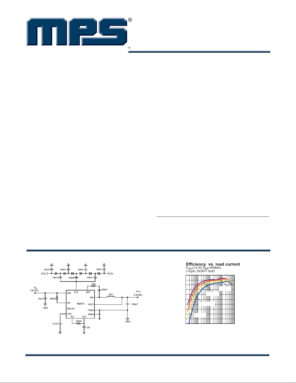
TYPICAL APPLICATION
100
95
90
85
80
75
70
65
EFFICIENCY (%)
60
55
50
NB670 Rev. 1.01 www.MonolithicPower.com 1
7/23/2013 MPS Proprietary Information. Patent Protected. Unauthorized Photocopy and Duplication Prohibited.
© 2013 MPS. All Rights Reserved.
V
=12.6V
IN
VIN=19V
1 10 100 1000 10000
OUTPUT CURRENT (A)
V
=6V
IN
=8.4V
V
IN
Page 2
NB670 ― 24V, HIGH CURRENT SYNCHRONOUS BUCK CONVERTER WITH LDO
y
ORDERING INFORMATION
Part Number* Package Top Marking
NB670GQ QFN16 (3mmx3mm) ADZ
* For Tape & Reel, add suffix –Z (e.g. NB670GQ–Z)
PACKAGE REFERENCE
TOP VIEW
VCC
AGND EN
ENLDO
12 11
1314
BST
10
VIN
ABSOLUTE MAXIMUM RATINGS
1
2PGND
3
NC
EXPOSED PAD
ON BACKSIDE
(1)
Supply Voltage VIN....................................... 24V
V
...............................................-0.3V to 24.3V
SW
(30ns)..........................................-3V to 28V
V
SW
V
(5ns)............................................-6V to 28V
SW
V
................................................... VSW + 5.5V
BST
............................................................... 12V
V
EN
V
Enable Current I
........................................................... 12V
ENLDO
(2)
................................ 2.5mA
EN
All Other Pins...............................-0.3V to +5.5V
Continuous Power Dissipation (T
=+25°C)
A
(3)
QFN16……………………..….…..…………1.8W
Junction Temperature...............................150°C
Lead Temperature ....................................260°C
Storage Temperature............... -65°C to +150°C
15
SW
16
54 6 7
CLKPG VOUT
Recommended Operating Conditions
Supply Voltage VIN.............................. 5V to 22V
Output Voltage V
Enable Current I
Operating Junction Temp. (T
Thermal Resistance
QFN16 (3mmx3mm)............... 70...... 15... °C/W
Notes:
1) Exceeding these ratings may damage the device.
2) Refer to Page 19 of Configuring the EN Control.
3) The maximum allowable power dissipation is a function of the
4) The device is not guaranteed to function outside of its
5) Measured on JESD51-7, 4-layer PCB.
9
SWSW
SW
8
LDO
................................... 3.3V
OUT
...................................... 1mA
EN
)..-40°C to +125°C
J
(5)
θ
maximum junction temperature T
ambient thermal resistance
. The maximum allowable continuous power dissipation at
T
A
any ambient temperature is calculated by P
)/JA. Exceeding the maximum allowable power dissipation
T
A
will cause excessive die temperature, and the regulator will go
into thermal shutdown. Internal thermal shutdown circuitr
protects the device from permanent damage.
operating conditions.
(MAX), the junction-to-
J
, and the ambient temperature
JA
θJC
JA
(MAX)=(TJ(MAX)-
D
(4)
NB670 Rev. 1.01 www.MonolithicPower.com 2
7/23/2013 MPS Proprietary Information. Patent Protected. Unauthorized Photocopy and Duplication Prohibited.
© 2013 MPS. All Rights Reserved.
Page 3
NB670 ― 24V, HIGH CURRENT SYNCHRONOUS BUCK CONVERTER WITH LDO
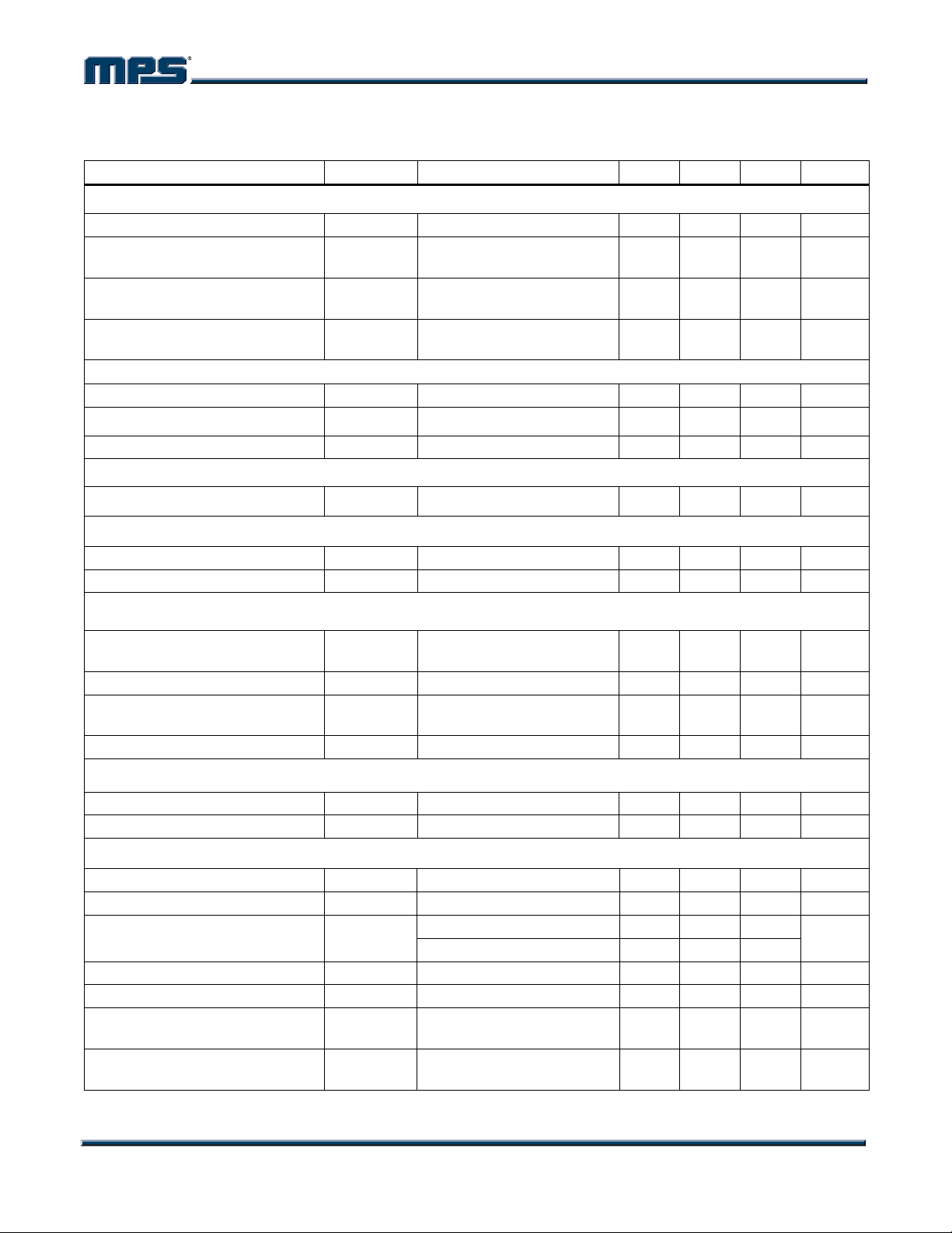
ELECTRICAL CHARACTERISTICS
VIN = 12V, TJ = 25°C, unless otherwise noted.
Parameters Symbol Condition Min Typ Max Units
Supply Current
Supply Current (Shutdown) I
Supply Current (Quiescent) IIN
Supply Current (No load) IIN
Supply Current (Standby) I
MOSFET
High-side Switch On Resistance HS
Low-side Switch On Resistance LS
Switch Leakage SW
Current Limit
VEN = 0V 1 2 A
IN_Shtdn
V
= 2V, V
EN
V
= 3.5V
OUT
V
= 2V, V
EN
V
= 3.35V, Io=0A
OUT
V
= 0V, V
EN
IN_Stby
RDS-ON
RDS-ON
LKG
I
= 0A
LDO
30 m
15 m
VEN = 0V, VSW = 0V 0 1 A
ENLDO
ENLDO
ENLDO
= 2V ,
= 2V ,
= 2V ,
140 220 300 A
240 A
40 80 120 A
Low-side Valley Current Limit I
8 8.5 9.5 A
LIMIT
Switching frequency and minimum off timer
Switching Frequency FSW 400 500 600 kHz
Minimum Off Time
(6)
T
350 ns
OFF
Over-voltage and Under-voltage Protection
OVP Threshold V
OVP Delay
(6)
T
UVP Threshold V
UVP Delay
(6)
T
OVP
OVPDEL
UVP
UVPDEL
125 130 135
2.5 s
55 60 65
8 s
%
V
OUT_Ref
%
V
OUT_Ref
Vout_Ref And Soft Start
Vout Ref Voltage Vout_Ref 3.285 3.35 3.415 V
Soft Start Time TSS 1.5 1.8 1.95 ms
Enable And UVLO
Enable Input Low Voltage VILEN 1.15 1.25 1.35 V
Enable Hysteresis V
Enable Input Current IEN
Enable LDO Input Low Voltage V
Enable LDO Hysteresis V
VCC Under Voltage Lockout
Threshold Rising
VCC Under Voltage Lockout
Threshold Hysteresis
ENLDO-HYS
VCC
VCC
100 mV
EN-HYS
VEN = 2V 5
V
= 0V 0
EN
1.15 1.25 1.35 V
ENLDO
A
100 mV
4.65 4.85 V
Vth
500 mV
HYS
NB670 Rev. 1.01 www.MonolithicPower.com 3
7/23/2013 MPS Proprietary Information. Patent Protected. Unauthorized Photocopy and Duplication Prohibited.
© 2013 MPS. All Rights Reserved.
Page 4
NB670 ― 24V, HIGH CURRENT SYNCHRONOUS BUCK CONVERTER WITH LDO
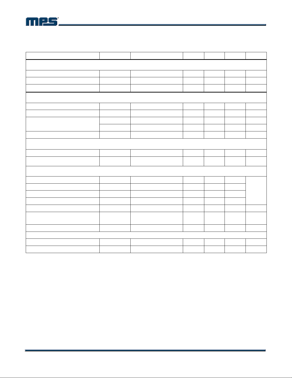
ELECTRICAL CHARACTERISTICS (continued)
VIN = 12V, TJ = 25°C, unless otherwise noted.
Parameters Symbol Condition Min Typ Max Units
CLK Output
CLK Output High Level Voltage V
CLK Output Low Level Voltage V
CLK Frequency F
I
CLKH
I
CLKL
CLK
= -5mA 3.1 3.25 3.4 V
Vclk
= 5mA 0 0.05 0.1 V
Vclk
T
= 25°C
J
300 kHz
LDO Regulator
LDO Regulator V
LDO Load Regulation
LDO Load Capability
Switch Rdson R
3.25 3.35 3.45 V
LDO
I
Switch
=50mA 5 %
LDO
Before switch-over 70 90 120 mA
After switch-over 100 mA
I
=50mA 1.7 2.2
LDO
VCC Regulator
VCC Regulator V
VCC Load Regulation
CC
4.95 5.15 5.35 V
Icc=5mA 5 %
Power Good
PG Rising (Good) PG
PG Falling (Fault) PG
PG Rising (Fault) PG
PG Falling (Good) PG
95
Vth-Hi
85
Vth-Lo
115
Vth-Hi
105
Vth-Lo
%
V
OUT_Ref
Power Good Lower to High Delay PGTd 0.5 ms
Power Good Sink Current
Capability
Power Good Leakage Current I
Sink 4mA 0.4 V
V
PG
VPG = 3.3V 100 nA
PG_LEAK
Thermal Protection
Thermal Shutdown
(6)
T
150 °C
SD
Thermal Shutdown Hysteresis 25 °C
Note:
6) Guaranteed by design.
NB670 Rev. 1.01 www.MonolithicPower.com 4
7/23/2013 MPS Proprietary Information. Patent Protected. Unauthorized Photocopy and Duplication Prohibited.
© 2013 MPS. All Rights Reserved.
Page 5
NB670 ― 24V, HIGH CURRENT SYNCHRONOUS BUCK CONVERTER WITH LDO
PIN FUNCTIONS
PIN # Name Description
Supply Voltage. The VIN pin supplies power for internal MOSFET and regulator. The
1 VIN
2 PGND Power Ground. Use wide PCB traces and multiple vias to make the connection.
3 NC Not connected.
4 PG
5 CLK 300kHZ CLK output to drive the external charge pump
6 LDO
7 VOUT
8, 9
Exposed Pad
15, 16
10 BST
11 VCC
12 ENLDO
13 EN
14 AGND Analog ground. The internal reference is referred to AGND.
SW
NB670 operates from a +5V to +24V input rail. An input capacitor is needed to
decouple the input rail. Use wide PCB traces and multiple vias to make the
connection.
Power good output. The output of this pin is an open drain signal and is high if the
output voltage is higher than 95% of the nominal voltage. There is a delay from Vout
95% to PGOOD goes high.
Internal 3.3V LDO output. Decouple with a minimum 4.7µF ceramic capacitor as
close to the pin as possible. X7R or X5R grade dielectric ceramic capacitors are
recommended for their stable temperature characteristics.
Once the output voltage of the Buck regulator is ready, it will switch over the LDO
output to save the power loss.
Output voltage sense. For the NB670, the output of the Buck regulator is fixed to
3.3V. VOUT pin is used to sense the output voltage of the Buck regulator, connect
this pin to the output capacitor of the regulator directly. This pin also acts as the
input of the 3.3V LDO switch over power input.
Keep the VOUT sensing trace far away from the SW node. Vias should also be
avoided on the VOUT sensing trace.
Switch Output. Connect this pin to the inductor and bootstrap capacitor. This pin is
driven up to the VIN voltage by the high-side switch during the on-time of the PWM
duty cycle. The inductor current drives the SW pin negative during the off-time. The
on-resistance of the low-side switch and the internal diode fixes the negative
voltage. Use wide and short PCB traces to make the connection. Try to minimize the
area of the SW pattern.
Bootstrap. A capacitor connected between SW and BST pins is required to form a
floating supply across the high-side switch driver.
Internal 5V LDO output. The driver and control circuits are powered from this
voltage. Decouple with a minimum 1µF ceramic capacitor as close to the pin as
possible. X7R or X5R grade dielectric ceramic capacitors are recommended for their
stable temperature characteristics.
100mA LDO and VCC enable pin. ENLDO is internally pulled up to high. Leave this
pin open to enable the LDO. Drive it low to turn off all the regulators .
Buck regulator and charge pump clock enable pin. EN is a digital input that turns the
Buck regulator and CLK on or off. When the power supply of the control circuit is
ready, drive EN high to turn on the Buck regulator and charge pump clock, drive it
low to turn them off.
NB670 Rev. 1.01 www.MonolithicPower.com 5
7/23/2013 MPS Proprietary Information. Patent Protected. Unauthorized Photocopy and Duplication Prohibited.
© 2013 MPS. All Rights Reserved.
Page 6
NB670 ― 24V, HIGH CURRENT SYNCHRONOUS BUCK CONVERTER WITH LDO
TYPICAL PERFORMANCE CHARACTERISTICS
Performance waveforms are tested on the evaluation board of the Design Example section.
=12V, V
V
IN
=3.3V, L=2µH, TJ=+25°C, unless otherwise noted.
OUT
100
95
90
85
80
75
70
65
EFFICIENCY (%)
60
VIN=19V
55
50
1 10 100 1000 10000
OUTPUT CURRENT (A) OUTPUT CURRENT (A)
2500
2000
1500
1000
POWER LOSS (mW)
500
0
01234567
OUTPUT CURRENT (A) OUTPUT CURRENT (A)
V
V
=12.6V
IN
V
=12.6V
IN
V
=19V
IN
V
IN
IN
=6V
=8.4V
VIN=6V
V
IN
=8.4V
2500
V
=6V
=19V
V
IN
VIN=8.4V
IN
2000
1500
1000
500
POWER LOSS (mW)
=12.6V
V
IN
0
0123456
100
VIN=6V
90
80
70
60
EFFICIENCY (%)
50
40
0.001 0.01 0.1 1 10
V
OUTPUT CURRENT (A)
Line Regulation Load Regulation
1
0.8
0.6
0.4
0.2
-0.2
-0.4
-0.6
LINE REGULATION (%)
-0.8
-1
I
=0A
OUT
I
=3A
OUT
0
=6A
I
OUT
5 7 9 11 13 15 17 19
INPUT VOLTAGE (V)
1
0.8
0.6
0.4
0.2
0
-0.2
-0.4
-0.6
LOAD REGULATION (%)
-0.8
-1
VIN=8.4V
0123456
V
V
=12.6V
IN
=19V
IN
VIN=19V
IN
=8.4V
V
V
=12.6V
IN
=6V
IN
Supply Current(Shutdown)
vs. Input Voltage
2.5
2
1.5
1
0.5
0
5 7 9 111315171921
INPUT VOLTAGE (V) INPUT VOLTAGE (V)
Supply Current(Quiescent )
vs. Input Voltage
220
215
210
205
200
195
190
579111315171921
No Load Current vs.
Input Voltage
265
260
255
250
245
240
235
230
579111315171921
INPUT VOLTAGE (V)
NB670 Rev. 1.01 www.MonolithicPower.com 6
7/23/2013 MPS Proprietary Information. Patent Protected. Unauthorized Photocopy and Duplication Prohibited.
© 2013 MPS. All Rights Reserved.
Page 7

NB670 ― 24V, HIGH CURRENT SYNCHRONOUS BUCK CONVERTER WITH LDO
TYPICAL PERFORMANCE CHARACTERISTICS (continued)
Performance waveforms are tested on the evaluation board of the Design Example section.
=12V, V
V
IN
=3.3V, L=2µH, TJ=+25°C, unless otherwise noted.
OUT
Input/Output Voltage Ripple
I
= 0A
OUT
Input/Output Voltage Ripple
I
= 6A
OUT
Power Good through VIN
Start-Up
I
= 6A
OUT
V
OUT(AC)
50mV/div.
V
IN(AC)
200mV/div.
V
SW
5V/div.
2A/div.
V
OUT
2V/div.
V
5V/div.
V
PG
5V/div.
5A/div.
I
L
Power Good through
VIN Shutdown
I
= 6A
OUT
IN
I
L
V
OUT(AC)
50mV/div.
V
IN(AC)
200mV/div.
V
SW
10V/div.
5A/div.
V
OUT
2V/div.
V
EN
5V/div.
V
PG
5V/div.
5A/div.
I
L
Power Good through
EN Start-Up
I
= 6A
OUT
I
L
V
OUT
2V/div.
V
5V/div.
V
5V/div.
5A/div.
V
OUT
2V/div.
V
5V/div.
V
5V/div.
10A/div.
IN
PG
I
L
Power Good through
EN Shut-Down
I
= 6A
OUT
EN
PG
I
L
Start-Up through VIN
I
= 0A
OUT
V
OUT
2V/div.
V
IN
5V/div.
V
SW
5V/div.
I
L
5A/div.
Start-Up through VIN
I
= 6A
OUT
V
OUT
2V/div.
V
IN
5V/div.
V
SW
10V/div.
I
L
5A/div.
Shut-Down through VIN
I
= 0A
OUT
V
OUT
2V/div.
V
IN
5V/div.
V
SW
5V/div.
I
L
5A/div.
NB670 Rev. 1.01 www.MonolithicPower.com 7
7/23/2013 MPS Proprietary Information. Patent Protected. Unauthorized Photocopy and Duplication Prohibited.
© 2013 MPS. All Rights Reserved.
Page 8

NB670 ― 24V, HIGH CURRENT SYNCHRONOUS BUCK CONVERTER WITH LDO
TYPICAL PERFORMANCE CHARACTERISTICS (continued)
Performance waveforms are tested on the evaluation board of the Design Example section.
=12V, V
V
IN
=3.3V, L=2µH, TJ=+25°C, unless otherwise noted.
OUT
Shut-Down through Vin
I
= 6A
OUT
Start-Up through EN
I
= 0A
OUT
Start-Up through EN
I
= 6A
OUT
V
OUT
2V/div.
V
5V/div.
V
SW
10V/div.
5A/div.
V
OUT
2V/div.
V
EN
5V/div.
V
SW
10V/div.
5A/div.
IN
I
L
Shut-Down through EN
I
= 0A
OUT
I
L
V
OUT
2V/div.
V
EN
5V/div.
V
SW
10V/div.
5A/div.
V
OUT
2V/div.
V
EN
5V/div.
V
SW
10V/div.
5A/div.
I
L
Shut-Down through EN
I
= 6A
OUT
I
L
V
OUT
2V/div.
V
5V/div.
V
SW
10V/div.
5A/div.
V
OUT(AC)
50mV/div.
2A/div.
EN
I
L
I
L
V
OUT
2V/div.
V
SW
10V/div.
5A/div.
Short Circuit Protection
I
L
10V/div.
Thermal Shutdown
I
=6A
OUT
V
OUT
2V/div.
V
SW
I
L
5A/div.
V
OUT
2V/div.
V
SW
10V/div.
5A/div.
Thermal Recovery
I
=6A
OUT
I
L
NB670 Rev. 1.01 www.MonolithicPower.com 8
7/23/2013 MPS Proprietary Information. Patent Protected. Unauthorized Photocopy and Duplication Prohibited.
© 2013 MPS. All Rights Reserved.
Page 9

NB670 ― 24V, HIGH CURRENT SYNCHRONOUS BUCK CONVERTER WITH LDO
BLOCK DIAGRAM
VCC
VIN
VOUT
EN
Soft-
star t
0.6V V
BSTR EG
POR &
Reference
REF
V
FB
Min off time
On T ime
One Shot
Gate
control
VIN
BST
SW
Logic
VOUT
1V
130% V
REF
SW
95% V
OVP
REF
60% V
OCP
POK
REF
Fault
logic
UVP
PGND
PG
AGND
CLK
CLK
generator
Vcc
Vcc
Regulator
LDO
Swi tch-over
VIN
LDO
Control
ENLDO
LDO
Figure 1—Functional Block Diagram
VOUT
NB670 Rev. 1.01 www.MonolithicPower.com 9
7/23/2013 MPS Proprietary Information. Patent Protected. Unauthorized Photocopy and Duplication Prohibited.
© 2013 MPS. All Rights Reserved.
Page 10

NB670 ― 24V, HIGH CURRENT SYNCHRONOUS BUCK CONVERTER WITH LDO
OPERATION
PWM Operation
The NB670 is fully integrated synchronous
rectified step-down switch mode converter.
Constant-on-time (COT) control is employed to
provide fast transient response and easy loop
stabilization. At the beginning of each cycle, the
high-side MOSFET (HS-FET) is turned ON when
the feedback voltage (V
voltage (V
), which indicates insufficient output
REF
voltage. The ON period is determined by the
output voltage and input voltage to make the
switching frequency fairy constant over input
voltage range.
After the ON period elapses, the HS-FET is
turned off, or becomes OFF state. It is turned ON
again when V
drops below V
FB
operation this way, the converter regulates the
output voltage. The integrated low-side MOSFET
(LS-FET) is turned on when the HS-FET is in its
OFF state to minimize the conduction loss. There
will be a dead short between input and GND if
both HS-FET and LS-FET are turned on at the
same time. It’s called shoot-through. In order to
avoid shoot-through, a dead-time (DT) is
internally generated between HS-FET off and LSFET on, or LS-FET off and HS-FET on.
An internal compensation is applied for COT
control to make a more stable operation even
when ceramic capacitors are used as output
capacitors, this internal compensation will then
improve the jitter performance without affect the
line or load regulation.
Heavy-Load Operation
) is below the reference
FB
. By repeating
REF
When the output current is high and the inductor
current is always above zero amps, it is called
continuous-conduction-mode (CCM). The CCM
mode operation is shown in Figure 2 shown.
When V
is below V
FB
, HS-FET is turned on for
REF
a fixed interval. When the HS-FET is turned off,
the LS-FET is turned on until next period.
In CCM mode operation, the switching frequency
is fairly constant and it is called PWM mode.
Light-Load Operation
With the load decrease, the inductor current
decrease too. Once the inductor current touch
zero, the operation is transition from continuousconduction-mode (CCM) to discontinuousconduction-mode (DCM).
The light load operation is shown in Figure 3.
When V
is below V
FB
, HS-FET is turned on for
REF
a fixed interval which is determined by one- shot
on-timer as equation 1 shown. When the HS-FET
is turned off, the LS-FET is turned on until the
inductor current reaches zero. In DCM operation,
the V
does not reach V
FB
when the inductor
REF
current is approaching zero. The LS-FET driver
turns into tri-state (high Z) whenever the inductor
current reaches zero. A current modulator takes
over the control of LS-FET and limits the inductor
current to less than -1mA. Hence, the output
capacitors discharge slowly to GND through LSFET. As a result, the efficiency at light load
condition is greatly improved. At light load
condition, the HS-FET is not turned ON as
frequently as at heavy load condition. This is
called skip mode.
At light load or no load condition, the output
drops very slowly and the NB670 reduces the
switching frequency naturally and then high
efficiency is achieved at light load.
Figure 2—Heavy Load Operation
NB670 Rev. 1.01 www.MonolithicPower.com 10
7/23/2013 MPS Proprietary Information. Patent Protected. Unauthorized Photocopy and Duplication Prohibited.
© 2013 MPS. All Rights Reserved.
Page 11

NB670 ― 24V, HIGH CURRENT SYNCHRONOUS BUCK CONVERTER WITH LDO
V
V
NOISE
SLOPE2
V
FB
V
REF
HS D river
Figure 3—Light Load Operation
As the output current increases from the light
load condition, the time period within which the
current modulator regulates becomes shorter.
The HS-FET is turned ON more frequently.
Hence, the switching frequency increases
correspondingly. The output current reaches the
critical level when the current modulator time is
zero. The critical level of the output current is
determined as follows:
I
OUT
−×
=
2LF V
×× ×
SW IN
(1)
IN OUT OUT
(V V ) V
It turns into PWM mode once the output current
exceeds the critical level. After that, the switching
frequency stays fairly constant over the output
current range.
Jitter and FB Ramp Slope
Jitter occurs in both PWM and skip modes when
noise in the V
ripple propagates a delay to the
FB
HS-FET driver, as shown in Figures 4 and 5.
Jitter can affect system stability, with noise
immunity proportional to the steepness of V
downward slope. However, V
ripple does not
FB
FB
’s
directly affect noise immunity.
V
V
NOISE
S L OPE1
J itter
V
FB
V
HS Driver
RE
F
Figure 4—Jitter in PWM Mode
Jitter
Figure 5—Jitter in Skip Mode
Selecting the Output Capacitors
The traditional constant-on-time control scheme
is intrinsically unstable if output capacitor’s ESR
is not large enough as an effective current-sense
resistor. Ceramic capacitors usually can not be
used as output capacitor.
Figure 6 shows an equivalent circuit in PWM
mode with the HS-FET off. To realize the stability,
the ESR value should be chosen as follow:
TT
SW ON
R
≥
ESR
T
is the switching period.
SW
R
FB
R
0.7 2
SW
VOUT
×π
C
L
OUT
+
(2)
V
OUT
ESR
CAP
Figure 6—Simplified Circuit in PWM Mode
The NB670 has built in internal ramp
compensation to make sure the system is stable
even without the help of output capacitor’s ESR;
and thus the pure ceramic capacitor solution can
be applicant. The pure ceramic capacitor solution
can significantly reduce the output ripple, total
BOM cost and the board area.
Configuring the EN Control
The NB670 has two enable pins to control the
on/off of the internal regulators.
ENLDO is used to enable or disable the whole
NB670 Rev. 1.01 www.MonolithicPower.com 11
7/23/2013 MPS Proprietary Information. Patent Protected. Unauthorized Photocopy and Duplication Prohibited.
© 2013 MPS. All Rights Reserved.
Page 12

NB670 ― 24V, HIGH CURRENT SYNCHRONOUS BUCK CONVERTER WITH LDO
chip. Once ENLDO is off, all the regulators
include Vcc will be off. ENLDO is internally pulled
high so it can be floated in the normal operation.
When ENLDO is pulled high, Pull En high to turn
on the Buck regulator also the charge pump clk,
and pull EN low to turn them off. Do not float the
EN pin.
See Table1 for the logics to control the regulators
Table 1—ENLDO/EN Control
State ENLDO EN VCC VOUT/CLK LDO
S0 1 1 ON ON ON
S3 1 0 ON OFF ON
S4/S5 0 0 OFF OFF OFF
Others 0 1 OFF OFF OFF
For automatic start-up the EN pin can be pulled
up to input voltage through a resistive voltage
divider. Choose the values of the pull-up resistor
(R
from Vin pin to EN pin) and the pull-down
UP
resistor (R
from EN pin to GND) to
DOWN
determine the automatic start-up voltage:
+
RR
−
=×
V1.35 (V)
IN START
For example, for R
V is set at 5.32V.
the
−IN START
UP
UP DOW N
R
DOWN
=150k and R
(3)
DOWN
=51k,
To avoid noise, a 10nF ceramic capacitor from
EN to GND is recommended.
There is an internal Zener diode on the EN pin,
which clamps the EN pin voltage to prevent it
from running away. The maximum pull up current
assuming a worst case 12V internal Zener clamp
should be less than 1mA.
Therefore, when EN is driven by an external logic
signal, the EN voltage should be lower than 12V;
when EN is connected with VIN through a pull-up
resistor or a resistive voltage divider, the
resistance selection should ensure the maximum
pull up current less than 1mA.
If using a resistive voltage divider and VIN higher
than 12V, the allowed minimum pull-up resistor
R
should meet the following equation:
UP
V(V) 12
−
IN
R(k) R (k)
ΩΩ
UP DOWN
12
−<
1( m A )
(4)
Especially, just using the pull-up resistor R
UP
(the
pull-down resistor is not connected), the
V is determined by input UVLO, and the
IN-START
minimum resistor value is:
R(k)
Ω>
UP
IN
1( m A )
(5)
V(V) 12
−
A typical pull-up resistor is 499k.
Soft Start
The NB670 employs soft start (SS) mechanism
to ensure smooth output during power-up. When
the EN pin becomes high, the internal reference
voltage ramps up gradually; hence, the output
voltage ramps up smoothly, as well. Once the
reference voltage reaches the target value, the
soft start finishes and it enters into steady state
operation.
If the output is pre-biased to a certain voltage
during startup, the IC will disable the switching of
both high-side and low-side switches until the
voltage on the internal reference exceeds the
sensed output voltage at the internal FB node.
3.3V Linear Regulator
There is a built-in 100-mA standby linear
regulator which outputs 3.3V.The 3.3V LDO is
intended mainly for auxiliary 3.3V supply for the
notebook system during standby mode.
Add a ceramic capacitor with a value between
4.7F and 22uF placed close to the LDO pins to
stabilize LDOs.
3.3V LDO Switch Over
When the output voltage becomes higher than
3.15V and the power good flag is generated,
internal 3.3V LDO regulator is shut off and the
LDO output is connected to Vout pin by the
internal switch over MOSFET. The 20us power
good deglitch time helps a switch over without
glitch.
CLK for Charge Pump
The 300kHZ CLK signal can be used to drive an
external charge pump circuit to generate
approximately 12-15V DC voltage. The CLK
voltage becomes available once the VIN is higher
than UVLO threshold. Example of charge pump
control circuit is shown in Figure 7.
NB670 Rev. 1.01 www.MonolithicPower.com 12
7/23/2013 MPS Proprietary Information. Patent Protected. Unauthorized Photocopy and Duplication Prohibited.
© 2013 MPS. All Rights Reserved.
Page 13

NB670 ― 24V, HIGH CURRENT SYNCHRONOUS BUCK CONVERTER WITH LDO
CLK
100nF 100nF
5V 12V/100mA
100nF 100nF 100nF
PGND
PGND PGND
Figure 7—Charge Pump Circuit
Power Good (PG)
The NB670 has power-good (PG) output used to
indicate whether the output voltage of the Buck
regulator is ready or not. The PG pin is the open
drain of a MOSFET. It should be connected to
or other voltage source through a resistor
V
CC
(e.g. 100k). After the input voltage is applied, the
MOSFET is turned on so that the PG pin is pulled
to GND before SS is ready. After FB voltage
reaches 95% of REF voltage, the PG pin is
pulled high after a delay. The PG delay time is
0.5ms.
When the FB voltage drops to 85% of REF
voltage, the PG pin will be pulled low.
Over Current Protection
NB670 has cycle-by-cycle over current limiting
control. The current-limit circuit employs a
"valley" current-sensing algorithm. The part uses
the Rds(on) of the low side MOSFET as a
current-sensing element. If the magnitude of the
current-sense signal is above the current-limit
threshold, the PWM is not allowed to initiate a
new cycle.
The trip level is fixed internally. The inductor
current is monitored by the voltage between GND
pin and SW pin. GND is used as the positive
current sensing node so that GND should be
connected to the source terminal of the bottom
MOSFET.
Since the comparison is done during the high
side MOSFET OFF and low side MOSFET ON
state, the OC trip level sets the valley level of the
inductor current. Thus, the load current at overcurrent threshold, I
, can be calculated as
OC
follows:
In an over-current condition, the current to the
load exceeds the current to the output capacitor;
thus the output voltage tends to fall off.
Eventually, it will end up with crossing the under
voltage protection threshold and shutdown.
Over/Under-Voltage Protection (OVP/UVP)
NB670 monitors output voltage to detect over
and under voltage. When the feedback voltage
becomes higher than 115% of the target voltage,
the controller will enter Dynamic Regulation
Period. During this period, the LS will off when
the LS current goes to -1A, this will then
discharge the output and try to keep it within the
normal range. If the dynamic regulation can not
limit the increasing of the Vo, once the feedback
voltage becomes higher than 130% of the
feedback voltage, the OVP comparator output
goes high and the circuit latches as the high-side
MOSFET driver OFF and the low-side MOSFET
driver turn on acting as an -1A current source.
When the feedback voltage becomes lower than
60% of the target voltage, the UVP comparator
output goes high if the UV still occurs after 26us
delay; then the fault latch will be triggered--latches HS off and LS on; the LS FET keeps on
until the inductor current goes zero.
UVLO Protection
The NB670 has under-voltage lock-out protection
(UVLO). When the VCC voltage is higher than
the UVLO rising threshold voltage, the part will
be powered up. It shuts off when the VIN voltage
is lower than the UVLO falling threshold voltage.
This is non-latch protection. The part is disabled
when the VCC voltage falls below 4.65V. If an
application requires a higher under-voltage
lockout (UVLO), use the EN pin as shown in
Figure 8 to adjust the input voltage UVLO by
using two external resistors. It is recommended
to use the enable resistors to set the UVLO
falling threshold (VSTOP) above 4.65V. The
rising threshold (VSTART) should be set to
provide enough hysteresis to allow for any input
supply variations.
Δ
I
=+
I I_ limit
OC
NB670 Rev. 1.01 www.MonolithicPower.com 13
7/23/2013 MPS Proprietary Information. Patent Protected. Unauthorized Photocopy and Duplication Prohibited.
© 2013 MPS. All Rights Reserved.
inductor
2
(6)
Page 14
NB670 ― 24V, HIGH CURRENT SYNCHRONOUS BUCK CONVERTER WITH LDO
R
R
UP
DOWN
VIN
EN Comparator
EN
NB670
Figure 8—Adjustable UVLO
Thermal Shutdown
Thermal shutdown is employed in the NB670.
The junction temperature of the IC is internally
monitored. If the junction temperature exceeds
the threshold value (typical 150ºC), the converter
shuts off. This is a non-latch protection. There is
about 25ºC hysteresis. Once the junction
temperature drops to about 125ºC, it initiates a
SS.
Output Discharge
NB670 discharges the output when EN is low, or
the controller is turned off by the protection
functions (UVP & OCP, OCP, OVP, UVLO, and
thermal shutdown). The part discharges outputs
using an internal 6 MOSFET.
NB670 Rev. 1.01 www.MonolithicPower.com 14
7/23/2013 MPS Proprietary Information. Patent Protected. Unauthorized Photocopy and Duplication Prohibited.
© 2013 MPS. All Rights Reserved.
Page 15

NB670 ― 24V, HIGH CURRENT SYNCHRONOUS BUCK CONVERTER WITH LDO
=
APPLICATION INFORMATION
Input Capacitor
The input current to the step-down converter is
discontinuous and therefore requires a capacitor
to supply the AC current to the step-down
converter while maintaining the DC input voltage.
Ceramic capacitors are recommended for best
performance and should be placed as close to
the VIN pin as possible. Capacitors with X5R and
X7R ceramic dielectrics are recommended
because they are fairly stable with temperature
fluctuations.
The capacitors must also have a ripple current
rating greater than the maximum input ripple
current of the converter. The input ripple current
can be estimated as follows:
VV
II (1 )
=× ×−
CIN OUT
OUT OUT
VV
IN IN
The worst-case condition occurs at V
where:
I
CIN
OUT
(8)
I2=
For simplification, choose the input capacitor with
an RMS current rating greater than half of the
maximum load current.
The input capacitance value determines the input
voltage ripple of the converter. If there is an input
voltage ripple requirement in the system, choose
the input capacitor that meets the specification.
The input voltage ripple can be estimated as
follows:
IV V
V(1)
Δ= × ×−
IN
OUT OUT OUT
FC V V
×
SW IN IN IN
Under worst-case conditions where V
1
V
Δ=×
IN
4F C
I
OUT
×
SW IN
Output Capacitor
The output capacitor is required to maintain the
DC output voltage. Ceramic or POSCAP
capacitors are recommended. The output voltage
ripple can be estimated as:
(7)
= 2V
IN
OUT
(9)
= 2V
IN
OUT
(10)
,
:
VV
V(1)(R )
Δ= ×− × +
OUT ESR
OUT OUT
FL V 8FC
×××
SW IN SW OUT
1
(11)
In the case of ceramic capacitors, the impedance
at the switching frequency is dominated by the
capacitance. The output voltage ripple is mainly
caused by the capacitance. For simplification, the
output voltage ripple can be estimated as:
VV
V(1)
Δ= ×−
OUT
8F LC V
OUT OUT
2
×××
SW OUT IN
(12)
In the case of POSCAP capacitors, the ESR
dominates the impedance at the switching
frequency. The ramp voltage generated from the
ESR is high enough to stabilize the system.
Therefore, an external ramp is not needed. A
minimum ESR value around 12m is required to
ensure stable operation of the converter. For
simplification, the output ripple can be
approximated as:
VV
V(1)R
Δ= ×− ×
OUT ESR
OUT OUT
FL V
×
SW IN
(13)
Maximum output capacitor limitation should be
also considered in design application. NB670 has
an around 1.8ms soft-start time period. If the
output capacitor value is too high, the output
voltage can’t reach the design value during the
soft-start time, and then it will fail to regulate. The
maximum output capacitor value C
O_MAX
can be
limited approximately by:
C(I I)T/V
O_MAX LIM_AVG OUT ss OUT
Where, I
LIM_AVG
is the average start-up current
during soft-start period. T
−× (14)
is the soft-start time.
ss
Inductor
The inductor is necessary to supply constant
current to the output load while being driven by
the switched input voltage. A larger-value
inductor will result in less ripple current that will
result in lower output ripple voltage. However, a
larger-value inductor will have a larger physical
footprint, higher series resistance, and/or lower
saturation current. A good rule for determining
the inductance value is to design the peak-topeak ripple current in the inductor to be in the
range of 30% to 40% of the maximum output
NB670 Rev. 1.01 www.MonolithicPower.com 15
7/23/2013 MPS Proprietary Information. Patent Protected. Unauthorized Photocopy and Duplication Prohibited.
© 2013 MPS. All Rights Reserved.
Page 16

NB670 ― 24V, HIGH CURRENT SYNCHRONOUS BUCK CONVERTER WITH LDO
current, and that the peak inductor current is
below the maximum switch current limit. The
inductance value can be calculated by:
VV
Where I
L(1)
is the peak-to-peak inductor ripple
L
OUT OUT
=×−
FI V
×Δ
SW L IN
(15)
current.
2. Put the input capacitors as close to the IN
and GND pins as possible.
3. Put the decoupling capacitor as close to the
VCC and AGND pins as possible. Place the
Cap close to AGND if the distance is long.
And place >3 Vias if via is required to reduce
the leakage inductance.
The inductor should not saturate under the
maximum inductor peak current, where the peak
inductor current can be calculated by:
VV
II (1 )
=+ ×−
LP OUT
OUT OUT
2F L V
×
SW IN
(16)
PCB Layout Guide
The following guidelines should be followed when
designing the PC board for the NB670:
1. The high current paths (GND, IN, and SW)
should be placed very close to the device
with short, direct and wide traces.
4. Keep the VOUT sensing trace far away from
the SW node.Vias should also be avoided on
the VOUT sensing trace.
5. Keep the BST voltage path (BST, C3, and
SW) as short as possible.
6. Keep the IN and GND pads connected with
large copper and use at least two layers for
IN and GND trace to achieve better thermal
performance. Also, add several Vias with
10mil_drill/18mil_copper_width close to the
IN and GND pads to help on thermal
dissipation.
7. AGND connects PGND with KELVIN
Connecting.
8. Four-layer layout is strongly recommended to
achieve better thermal performance.
Note:
Please refer to the PCB Layout Application Note
for more details.
NB670 Rev. 1.01 www.MonolithicPower.com 16
7/23/2013 MPS Proprietary Information. Patent Protected. Unauthorized Photocopy and Duplication Prohibited.
© 2013 MPS. All Rights Reserved.
Page 17

NB670 ― 24V, HIGH CURRENT SYNCHRONOUS BUCK CONVERTER WITH LDO
AGND KELVIN
CONNECT TO PGND
AGND
EN
ENLDO
VIN
1314 12 11
1
15
2
16
3
PG
CLK
54 6 7
LDO
10
SW
9
8
VOUT
VOUT
GND
DO NOT CONNECT
TO AGND HERE
Figure 9—Recommend Layout
Recommend Design Example
A typical application schematic is shown in
Figure 10 when large ESR caps are used, and
Figure 11 shows the schematic when low ESR
caps are applied. The typical performance and
VOUT
circuit waveforms have been shown in the
Typical Performance Characteristics section. For
more possible applications of this device, please
refer to related Evaluation Board Datasheets.
NB670 Rev. 1.01 www.MonolithicPower.com 17
7/23/2013 MPS Proprietary Information. Patent Protected. Unauthorized Photocopy and Duplication Prohibited.
© 2013 MPS. All Rights Reserved.
Page 18
NB670 ― 24V, HIGH CURRENT SYNCHRONOUS BUCK CONVERTER WITH LDO
TYPICAL APPLICATION
Figure 10---Typical Application Circuit With Poscap
NB670 Vin=4.8-22V, Vout=3.3V, Iout=6A, Fsw=500kHz
Figure 11---Typical Application Circuit With Low ESR Ceramic Capacitor
NB670 Vin=4.8-22V, Vout=3.3V, Iout=6A, Fsw=500kHz
NB670 Rev. 1.01 www.MonolithicPower.com 18
7/23/2013 MPS Proprietary Information. Patent Protected. Unauthorized Photocopy and Duplication Prohibited.
© 2013 MPS. All Rights Reserved.
Page 19

NB670 ― 24V, HIGH CURRENT SYNCHRONOUS BUCK CONVERTER WITH LDO
PACKAGE INFORMATION
PIN 1 ID
MARKING
PIN 1 ID
INDEX AREA
QFN16 (3X3mm)
PIN 1 ID
0.10x45
癟 YP.
TOP VIEW
SIDE VIEW
0.10x45°
RECOMMENDED LAND PATTERN
BOTTOM VIEW
NOTE:
1) AL L DI ME NSI ONS ARE I N MI LL IM ETERS.
2) EXPOSED PADDLE SI ZE DOES NOT INCLUDE
MOLD FLASH.
3) L EAD COPLANARITY SHALL BE 0.10
MILLIMETERS MAX.
4) JEDEC REFERE NCE I S M O-220 .
5) DRAWING I S NOT TO SCALE .
NOTICE: The information in this document is subject to change without notice. Users should warrant and guarantee that third
party Intellectual Property rights are not infringed upon when integrating MPS products into any application. MPS will not
assume any legal responsibility for any said applications.
NB670 Rev. 1.01 www.MonolithicPower.com 19
7/23/2013 MPS Proprietary Information. Patent Protected. Unauthorized Photocopy and Duplication Prohibited.
© 2013 MPS. All Rights Reserved.
Page 20

 Loading...