

Page 1
© Semiconductor Components Industries, LLC, 2012
February, 2012 − Rev. 2
1 Publication Order Number:
EVBUM2077/D
NB4N527SMNEVB
Evaluation Board User's
Manual for NB4N527S
INTRODUCTION
ON Semiconductor has developed an evaluation board for
the NB4N527S device as a convenience for the customers
interested in performing their own device engineering
assessment. This board provides a high bandwidth 50 W
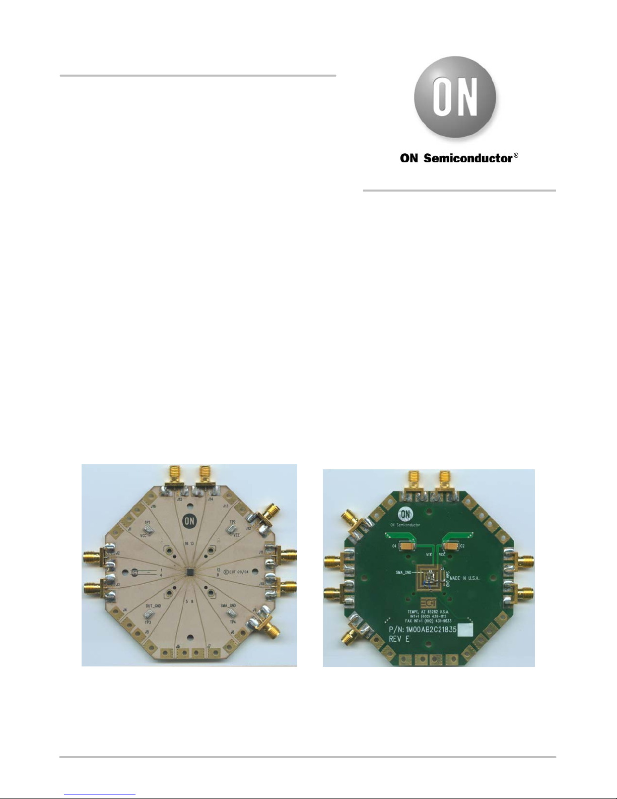
controlled impedance environment. The pictures in Figure 1
show the top and bottom view of the evaluation board, which
can be configured in several different ways.
This evaluation board manual contains:
• Information on 16−lead QFN Evaluation Board
• Assembly Instructions
• Appropriate Lab Setup
• Bill of Materials
This manual should be used in conjunction with the
NB4N527S device data sheet, which contains full technical
details on the device specifications and operation.
Board Lay−Up
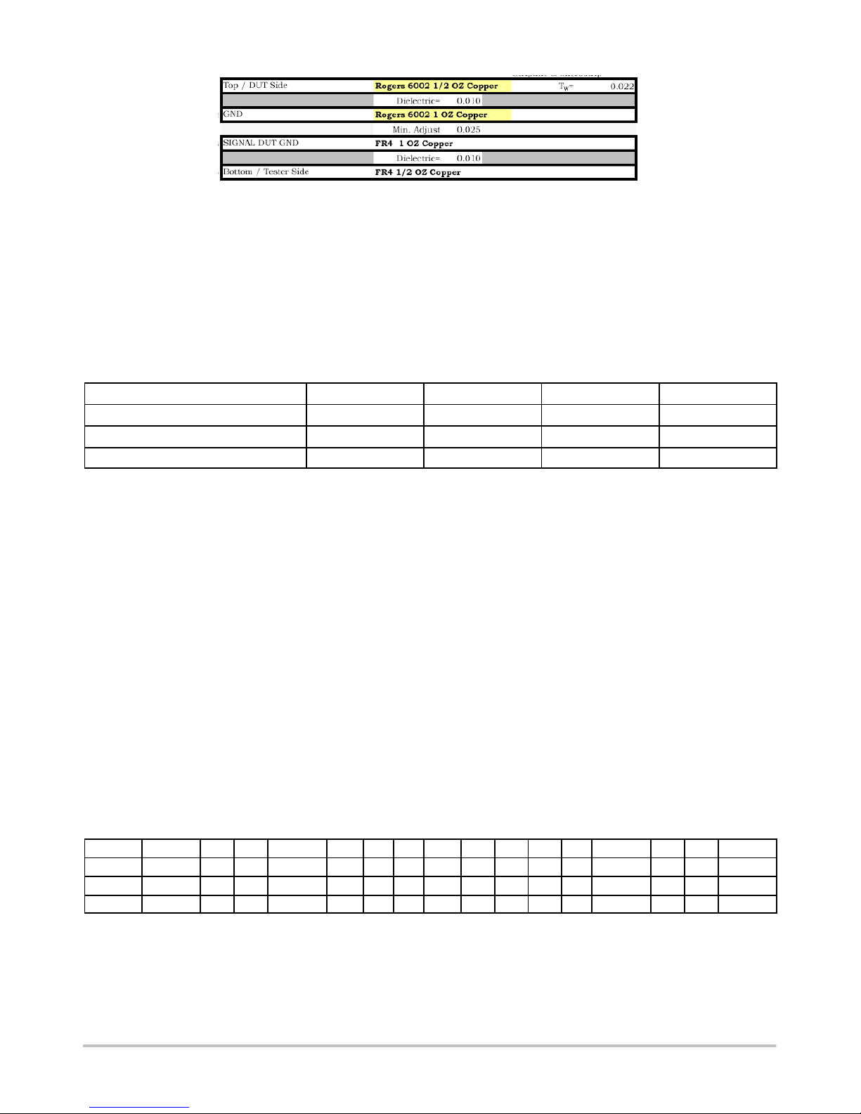
The 16−lead QFN evaluation board is implemented in
four layers with split (dual) power supplies (Figure 2,
Evaluation Board Lay−up). For standard lab setup, a split
(dual) power supply is essential to enable the 50 W internal
impedance in the oscilloscope as a device termination. The
first layer or primary trace layer is 0.005, thick Rogers
RO6002 material, which is designed to have equal electrical
length on all signal traces from the device under the test
(DUT) to the sense output. The second layer is the 1.0 oz.
copper ground plane. The FR4 dielectric material is placed
between the second and third layer, and between the third
and fourth layer. The third layer is also a 1.0 oz copper
ground plane. The fourth layer is the secondary trace layer.
Top View Bottom View
Figure 1. Top and Bottom View of the 16 QFN Evaluation Board
http://onsemi.com
EVAL BOARD USER’S MANUAL
Page 2
NB4N527SMNEVB
http://onsemi.com
2
Figure 2. Evaluation Board Lay−up
Connecting Power and Ground Planes
Top side of the evaluation board has the four surfaces
mount test point clips labeled V
CC
, VEE, SMA_GND, and
DUT_GND. DUT_GND is connected to the exposed flag of
the QFN package. For proper operation, the exposed flag is
recommended to be ELECTRICALLY left floating or tied
to V
EE
, but must be THERMALLY connected to a
sufficient heat conduit such as a thermal plane Exact supply
voltage values that need to be applied can be found in
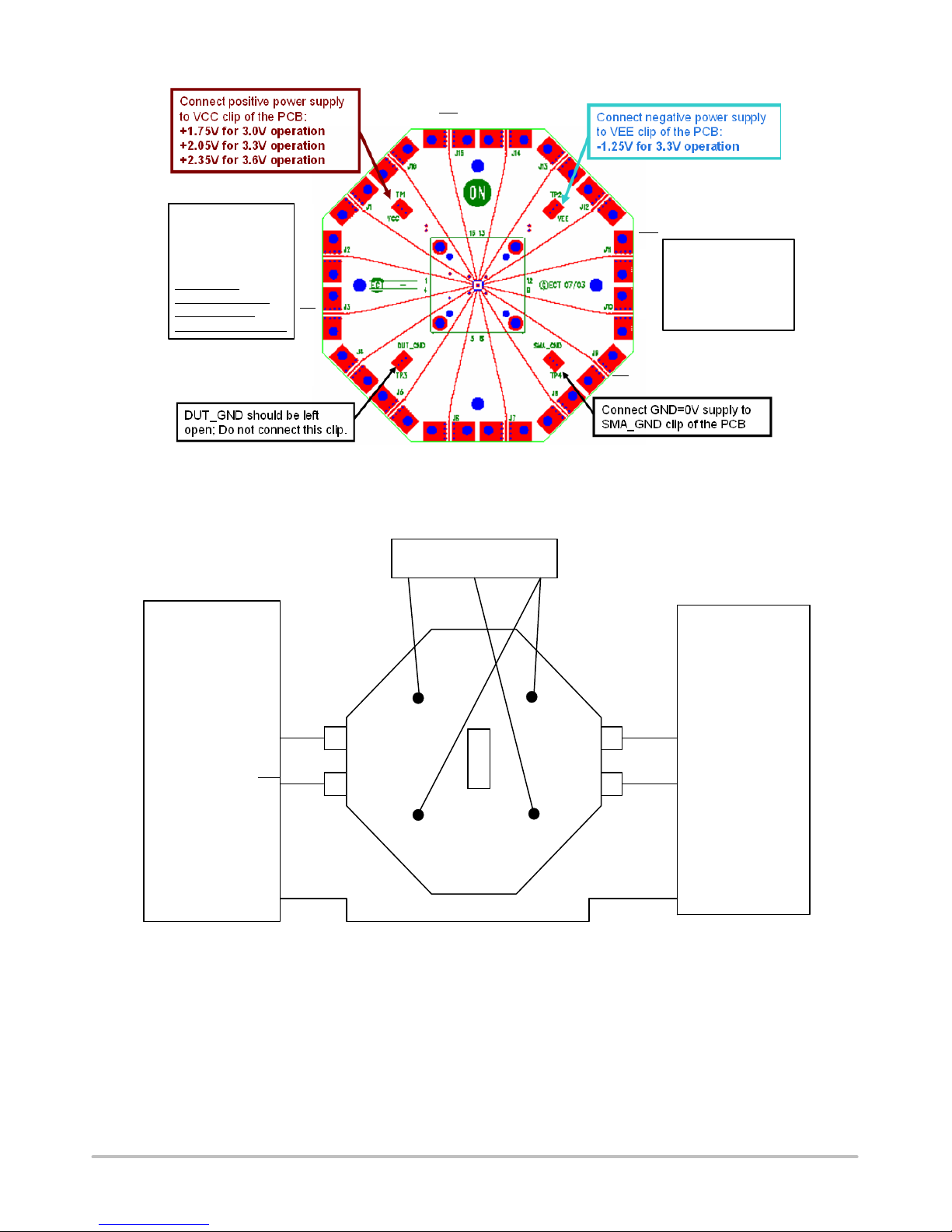
Table 1 and Figures 4 and 5.
Table 1. Power Supply Levels
Power Supply Span V
CC
V
EE
SMA_GND DUT_GND
3.0 V 1.75 V −1.25 V 0 V Float or V
EE
3.3 V 2.05 V −1.25 V 0 V Float or V
EE
3.6 V 2.35 V −1.25 V 0 V Float or V
EE
Stimulus (Generator) Termination
All ECL outputs need to be terminated to V
TT
(VTT = V
CC
–2.0 V = GND) via a 50 W resistor. The current board design
utilizes the internal resistors and the V
TDx
pins are wired to
ground. (More information on termination is provided in
AN8020). If evaluation does not require use of internal
termination resistors, 0402 chip resistor pads are provided
on the bottom side of the evaluation board. The jumper wires
of the V
TDx
pin pads should be removed (J1, J4, J13 and J15
to SMA_GND jumper). Solder the chip resistors to the
bottom side of the board between the appropriate input of the
device pin pads and the ground pads (for split power supply
setup).
Likewise for CML outputs, CML stimulus signal need to
be terminated to V
CC
via a 50 W resistor. If internal resistors
are used, the V
TDx
pin pads should be wired to VCC. To
accomplish this configuration, the jumper wire has to be
moved from SMA_GND ring to V
CC
ring on the bottom of
the board.
For the LVDS configuration, V
TDx
pin pads of the D0 or
D1 input has to be shorted to form 100 W across differential
lines. This configuration is accomplished by moving the
jumper wire from SMA_GND ring to complementary V
TDx
pin pad (example: VTD0 and VTD0b for D0 input and
VTD1 and VTD1b for D1 input).
DUT Termination
For standard lab setup and test, a split (dual) power supply
is required enabling the 50 W internal impedance in the
oscilloscope to be used as a termination of the signals (in
split power supply setup SMA_GND is the system ground,
V
CC
is varied, and VEE is –1.25 V; see Table 1, Power
Supply Levels).
Board Components Configuration
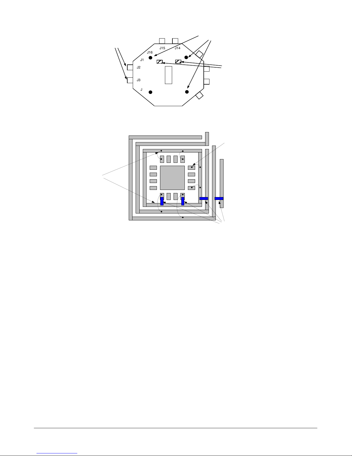
The NB4N527SMNEVB evaluation board requires eight
side SMA connectors. Placement locations are described in
Table 2 and Figure 3.
Table 2. SMA Connectors and Jumpers Placement
Device J1 J2 J3 J4 J5 J6 J7 J8 J9 J10 J11 J12 J13 J14 J15 J16
Pin # 1 2 3 4 5 6 7 8 9 10 11 12 13 14 15 16
Connector No Yes Yes No No No No No Ye s Yes Yes No No Yes Yes No
Wire SMA_GND No No SMA_GND V
EE
No No V
CC
No No No No SMA_GND No No SMA_GND
Page 3
NB4N527SMNEVB
http://onsemi.com
3
J14J15
J16
J1
J2
J3
J4
J5
J6 J7
J8
J9
J10
J11
J12
J13
D
U
T
4 x Surface Mount Test
Points
2 x 10 mF Decoupling
Capacitors on the back of
the PCB (C4, C2)
8 x SMA Connectors
Top View
SMA_GND
VCC
VEE
Pin 1
Pad
Wire
DUT_GND
SMA_GND
4 x 0.01 mF or 0.1 mF
Decoupling Capacitors
(C1, C3, C5, C6)
Bottom View
Figure 3. Components Placement
C4 C2
Page 4
NB4N527SMNEVB
http://onsemi.com
4
Figure 4. Lab Setup for NB4N527S
DODO
QO
QO
Q1
Q1
Connect output of
the generator to the
input pins labeled
J2, J3, J14, J15
(D0/D0B, D1/D1B)
Note: Internal
termination pins are
connected to the
SMA GND on the PCB.
D1
D1
Connect outputs of
the device labeled
J9, J10, J11 and J12
(Q0/Q0B, Q1/Q1B)
directly to the scope
head.
Power Supply
VCC GND VEE
D
U
T
Differential
Signal
Generator
Test
Measuring
Equipment
Channel 1
Channel 2
Trigger
Trigger
Out
Out
Figure 5. Simplified Equipment Lab Setup Block Diagram
1. Connect appropriate power supplies to VCC, VEE,
SMA_GND, and SMA_DUT.
2. Connect a signal generator to the input SMA
connectors. Setup input signal according to the
device data sheet.
3. Connect a test measurement device on the device
output SMA connectors.
NOTE: The test measurement device must contain 50 W
termination.
Page 5

NB4N527SMNEVB
http://onsemi.com
5
Table 3. Bill of Materials
Components Manufacturer Description Part Number Qty. Web Site
SMA
Connector
Johnson*
Rosenberger
SMA Connector,
Side Launch, Gold
Plated
142−0701−851
32K243−40ME3
8 http://www.johnsoncomponents.com
http://www.rosenbergerna.com
Surface Mount
Test Points
Keystone* SMT Miniature Test
Point
5015 4 http://www.keyelco.com
Chip
Capacitor
AVC
Corporation*
0603 0.01 mF "
10%
10 mF " 10%
06035C103KAT2A
T491C106K016AS
4
2
http://www.avxcorp.com
Chip Resistor Panasonic*
0402 50 W " 1%
Presicion Thick
Film Chip Resistor
ERJ−2RKF49R9X Optional** http://www.panasonic.com
Evaluation
Board
ON
Semiconductor
QFN 16 Evaluation
Board
ECLQFN16EVB 1 http://www.onsemi.com
Device
Samples
ON
Semiconductor
QFN 16 Package
Device
NB4N527SMN 1 http://www.onsemi.com
*Components are available through most distributors, i.e. www.newark.com, www.Digikey.com
Page 6
NB4N527SMNEVB
http://onsemi.com
6
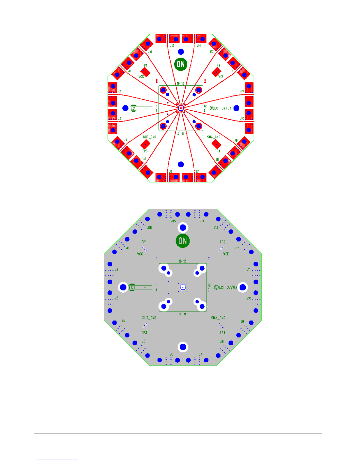
Top Layer
Second Layer (SMA_GND Plane)
Figure 6. Gerber Files
Page 7
NB4N527SMNEVB
http://onsemi.com
7
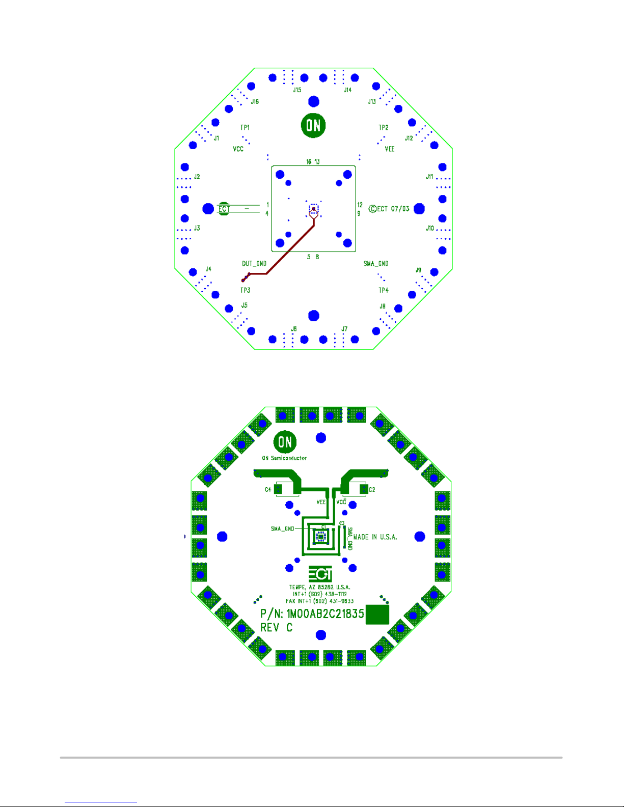
Third Layer (DUT_GND Trace)
Bottom Layer
Figure 7. Gerber Files
Page 8

NB4N527SMNEVB
http://onsemi.com
8
ON Semiconductor and are registered trademarks of Semiconductor Components Industries, LLC (SCILLC). SCILLC reserves the right to make changes without further notice
to any products herein. SCILLC makes no warranty, representation or guarantee regarding the suitability of its products for any particular purpose, nor does SCILLC assume any liability
arising out of the application or use of any product or circuit, and specifically disclaims any and all liability, including without limitation special, consequential or incidental damages.
“Typical” parameters which may be provided in SCILLC data sheets and/or specifications can and do vary in different applications and actual performance may vary over time. All
operating parameters, including “Typicals” must be validated for each customer application by customer’s technical experts. SCILLC does not convey any license under its patent rights
nor the rights of others. SCILLC products are not designed, intended, or authorized for use as components in systems intended for surgical implant into the body, or other applications
intended to support or sustain life, or for any other application in which the failure of the SCILLC product could create a situation where personal injury or death may occur. Should
Buyer purchase or use SCILLC products for any such unintended or unauthorized application, Buyer shall indemnify and hold SCILLC and its officers, employees, subsidiaries, affiliates,
and distributors harmless against all claims, costs, damages, and expenses, and reasonable attorney fees arising out of, directly or indirectly, any claim of personal injury or death
associated with such unintended or unauthorized use, even if such claim alleges that SCILLC was negligent regarding the design or manufacture of the part. SCILLC is an Equal
Opportunity/Affirmative Action Employer. This literature is subject to all applicable copyright laws and is not for resale in any manner.
EVBUM2077/D
PUBLICATION ORDERING INFORMATION
N. American Technical Support: 800−282−9855 Toll Free
USA/Canada
Europe, Middle East and Africa Technical Support:
Phone: 421 33 790 2910
Japan Customer Focus Center
Phone: 81−3−5817−1050
LITERATURE FULFILLMENT:
Literature Distribution Center for ON Semiconductor
P.O. Box 5163, Denver, Colorado 80217 USA
Phone: 303−675−2175 or 800−344−3860 Toll Free USA/Canada
Fax: 303−675−2176 or 800−344−3867 Toll Free USA/Canada
Email: [email protected]
ON Semiconductor Website: www.onsemi.com
Order Literature: http://www.onsemi.com/orderlit
For additional information, please contact your local
Sales Representative
Page 9

Mouser Electronics
Authorized Distributor
Click to View Pricing, Inventory, Delivery & Lifecycle Information:
ON Semiconductor:
NB4N527SMNEVB
 Loading...