

*Other brands and names are the property of their respective owners.
Information in this document is provided in connection with Intel products. Intel assumes no liability whatsoever, including infringement of any patent or
copyright, for sale and use of Intel products except as provided in Intel’s Terms and Conditions of Sale for such products. Intel retains the right to make
changes to these specifications at any time, without notice. Microcomputer Products may have minor variations to this specification known as errata.
September 1994COPYRIGHT©INTEL CORPORATION, 1995 Order Number: 272267-004
8XC196NT
CHMOS MICROCONTROLLER WITH
1 MBYTE LINEAR ADDRESS SPACE
Y
20 MHz Operation
Y
High Performance CHMOS 16-Bit CPU
Y
Up to 32 Kbytes of On-Chip OTPROM
Y
Up to 1 Kbyte of On-Chip Register RAM
Y
Up to 512 Bytes of Internal RAM
Y
Register-Register Architecture
Y
4 Channel/10-Bit A/D with Sample/Hold
Y
37 Prioritized Interrupt Sources
Y
Up to Seven 8-Bit (56) I/O Ports
Y
Full Duplex Serial I/O Port
Y
Dedicated Baud Rate Generator
Y
Interprocessor Communication Slave
Port
Y
Selectable Bus Timing Modes for
Flexible External Memory Interfacing
Y
Oscillator Fail Detection Circuitry
Y
High Speed Peripheral Transaction
Server (PTS)
Y
Two Dedicated 16-Bit High-Speed
Compare Registers
Y
10 High Speed Capture/Compare (EPA)
Y
Full Duplex Synchronous Serial I/O
Port (SSIO)
Y
Two Flexible 16-Bit Timer/Counters
Y
Quadrature Counting Inputs
Y
Flexible 8-/16-Bit External Bus
(Programmable)
Y
Programmable Bus (HOLD/HLDA)
Y
1.4 ms 16 x 16 Multiply
Y
2.4 ms 32/16 Divide
Y
68-Pin Package
Device Pins/Package OTPROM
Reg Code Address
I/O EPA A/D
RAM RAM Space
8XC196NT 68P PLCC 32K 1K 512 1 Mbyte 56 10 4
Xe7 OTPROM Device
X
e
0 ROMLESS
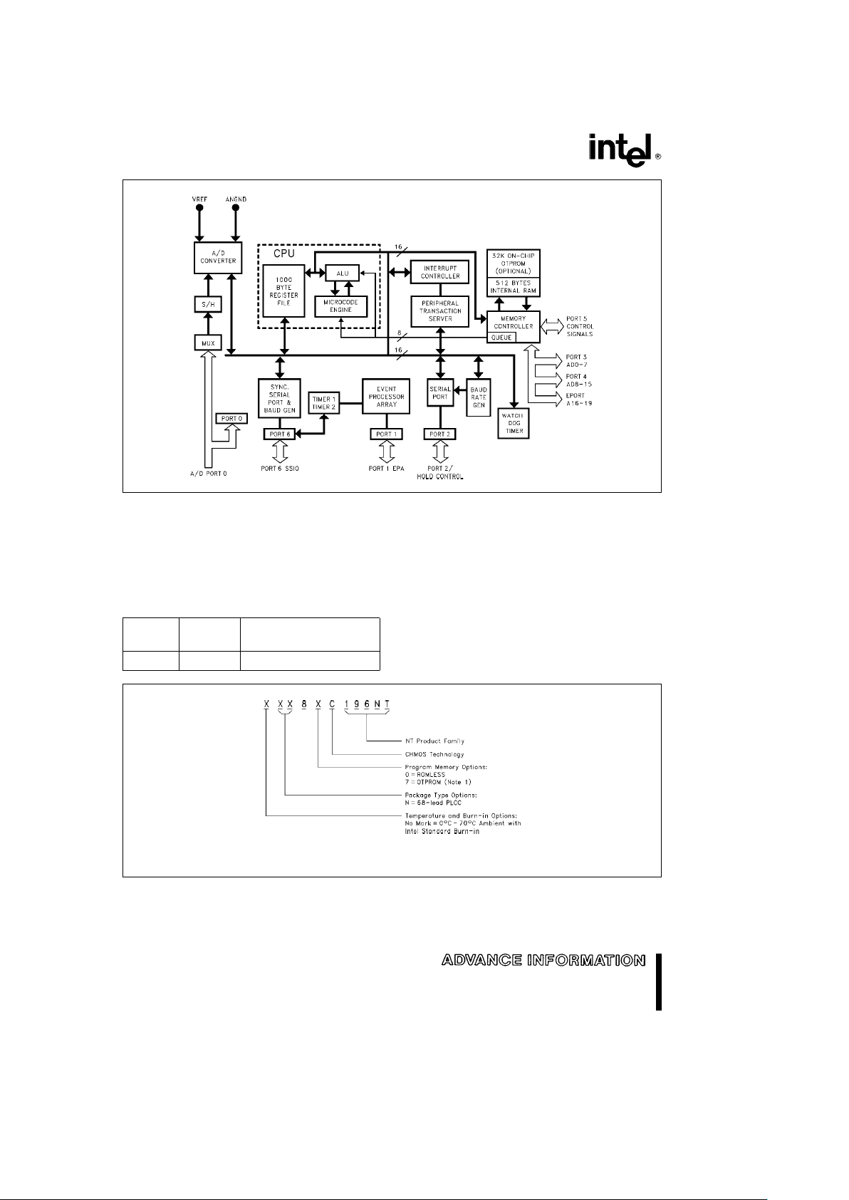
The 8XC196NT 16-bit microcontroller is a high performance member of the MCSÉ96 microcontroller family.
The 8XC196NT is an enhanced 8XC196KR device with 1 Mbyte of linear address space, 1000 bytes of
register RAM, 512 bytes of internal RAM, 20 MHz operation and an optional 32 Kbytes of OTPROM. Intel’s
CHMOS III-E process provides a high performance processor along with low power consumption.
Ten high-speed capture/compare modules are provided. As capture modules event times with 200 ns resolution can be recorded and generate interrupts. As compare modules events such as toggling of a port pin,
starting an A/D conversion, pulse width modulation, and software timers can be generated. Events can be
based on the timer or up/down counter.
8XC196NT
272267– 1
Figure 1. 8XC196NT Block Diagram
PROCESS INFORMATION
This device is manufactured on P629.5, a CHMOS
III-E process. Additional process and reliability information is available in Intel’s
Components Quality
and Reliability Handbook
, Order Number 210997.
Table 1. Thermal Characteristics
Package
i
JA
i
JC
Type
PLCC 36.5§C/W 13§C/W
All thermal impedance data is approximate for static
air conditions at 1W of power dissipation. Values will
change depending on operation conditions and application. See the Intel
Packaging Handbook
(order
number 240800) for a description of Intel’s thermal
impedance test methodology.
272267– 2
EXAMPLE: N87C196NT is 68-Lead PLCC OTPROM.
For complete package dimensional data, refer to the Intel Packaging Handbook (Order Number 240800).
Figure 2. The 8XC186NT Familiy Nomenclature
2
8XC196NT
8XC196NT Memory Map
Address
Description
(Note 7)
FFFFFFH
External Memory
FFA000H
FF9FFFH Internal OTPROM or External Memory (Determined by EA Pin)
FF2080H RESET at FF2080H
FF207FH Reserved Memory (Internal OTPROM or External Memory)
FF2000H (Determined by EA
Pin)
FF1FFFH
External Memory
FF0600H
FF05FFH
Internal RAM (Identically Mapped into 00400H–005FFH)
FF0400H
FF03FFH
External Memory
FF0100H
FF00FFH
Reserved for ICE
FF0000H
FEFFFFH
External Memory for future devices
100000H
FFFFFH
984 Kbytes External Memory
00A000H
009FFFH
Internal OTPROM or External Memory (Note 1)
002080H
00207FH Reserved Memory (Internal OTPROM or External Memory)
002000H (Notes 1, 3, and 6)
001FFFH
Memory Mapped Special Function Registers (SFR’s)
001FE0H
001FDFH
Internal Special Function Registers (SFR’s) (Note 5)
001F00H
001EFFH
External Memory
000600H
0005FFH Internal RAM
000400H (Address with Indirect or Indexed Modes)
0003FFH
Upper Register File (Address with Indirect or
Register RAM
Indexed Modes or through Windows.) (Note 2)
000100H
*
0000FFH
Register RAM
Lower Register File
000018H (Address with Direct,
000017H
CPU SFR’s
Indirect, or Indexed
000000H *
Modes.) (Notes 2, 4)
NOTES:
1. These areas are mapped internal OTPROM if the REMAP bit (CCB2.2) is set and EA
e
5V. Otherwise they are external
memory.
2. Code executed in locations 00000H to 003FFH will be forced external.
3. Reserved memory locations must contain 0FFH unless noted.
4. Reserved SFR bit locations must be written with 0.
5. Refer to 8XC196NT User’s Guide and Quick Reference for SFR descriptions.
6. WARNING: The contents or functions of reserved memory locations may change with future revisions of the device.
Therefore, a program that relies on one or more of these locations may not function properly.
7. The 8XC196NT internally uses 24 bit address, but only 20 address lines are bonded out allowing 1 Mbyte external
address space.
3
8XC196NT
272267– 3
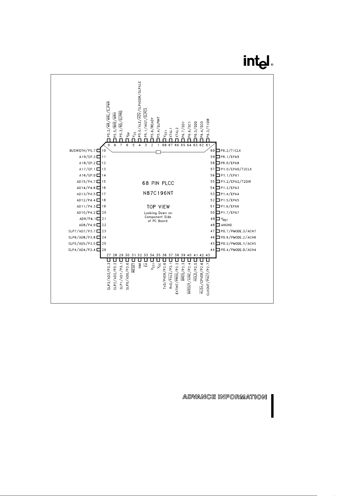
Figure 3. 68-Pin PLCC Package Diagram
4
8XC196NT
PIN DESCRIPTIONS
Symbol Name and Function
V
CC
Main supply voltage (a5V).
VSS,V
SS1,VSS1
Digital circuit ground (0V). There are multiple VSSpins, all of which MUST be
connected.
V
REF
Reference for the A/D converter (a5V). V
REF
is also the supply voltage to the
analog portion of the A/D converter and the logic used to read Port 0. Must be
connected for A/D and Port 0 to function.
V
PP
Programming voltage for the OTPROM parts. It should bea12.5V for programming.
It is also the timing pin for the return from powerdown circuit. Connect to V
CC
if
powerdown not being used.
ANGND Reference ground for the A/D converter. Must be held at nominally the same
potential as V
SS
.
XTAL1 Input of the oscillator inverter and the internal clock generator.
XTAL2 Output of the oscillator inverter.
P2.7/CLKOUT Output of the internal clock generator. The frequency is (/2 the oscillator frequency.
It has a 50% duty cycle. Also LSIO pin.
RESET Reset input to and open-drain output from the chip. RESET has an internal pullup.
P5.7/BUSWIDTH Input for bus width selection. If CCR bit 1 is a one and CCR1 bit 2 is a one, this pin
dyamically controls the Buswidth of the bus cycle in progress. If BUSWIDTH is low,
an 8-bit cycle occurs, if BUSWIDTH is high, a 16-bit cycle occurs. If CCR bit 1 is ‘‘0’’
and CCR1 bit 2 is ‘‘1’’, all bus cycles are 8-bit, if CCR bit 1 is ‘‘1’’ and CCR1 bit 2 is
‘‘0’’, all bus cycles are 16-bit. CCR bit 1
e
‘‘0’’ and CCR1 bit 2e‘‘0’’ is illegal. Also
an LSIO pin when not used as BUSWIDTH.
NMI A positive transition causes a non maskable interrupt vector through memory
location 203EH.
P5.1/INST/SLPCS Output high during an external memory read indicates the read is an instruction
fetch. INST is valid throughout the bus cycle. INST is active only during external
memory fetches, during internal OTPROM fetches INST is held low. Also LSIO when
not INST. SLPCS
is the Slave Port Chip Select.
EA Input for memory select (External Access). EA equal to a high causes memory
accesses to locations 0FF2000H through 0FF9FFFH to be directed to on-chip
OTPROM. EA
equal to a low causes accesses to these locations to be directed to
off-chip memory. EA
ea
12.5V causes execution to begin in the Programming
Mode. EA
is latched at reset.
HOLD Bus Hold Input requesting control of the bus.
HLDA Bus Hold acknowledge output indicating release of the bus.
BREQ Bus Request output activated when the bus controller has a pending external
memory cycle.
P5.0/ALE/ADV/ Address Latch Enable or Address Valid output, as selected by CCR. Both pin
options provide a latch to demultiplex the address from the address/data bus. When
SLPADDR/
the pin is ADV
, it goes inactive (high) at the end of the bus cycle. ADV can be used
SLPALE
as a chip select for external memory. ALE/ADV
is active only during external
memory accesses. Also LSIO when not used as ALE. SLPADDR is the Slave Port
Address Control Input and SLPALE is the Slave Port Address Latch Enable Input.
P5.3/RD/SLPRD Read signal output to external memory. RD is active only during external memory
reads or LSIO when not used as RD. SLPRD is the Slave Port Read Control Input.
5
8XC196NT
PIN DESCRIPTIONS (Continued)
Symbol Name and Function
P5.2/WR/WRL/SLPWR Write and Write Low output to external memory, as selected by the CCR, WR
will go low for every external write, while WRL will go low only for external
writes where an even byte is being written. WR
/WRL is active during external
memory writes. Also an LSIO pin when not used as WR
/WRL. SLPWR is the
Slave Port Write Control Input
P5.5/BHE/WRH Byte High Enable or Write High output, as selected by the CCR. BHEe0
selects the bank of memory that is connected to the high byte of the data bus.
A0
e
0 selects that bank of memory that is connected to the low byte. Thus
accesses to a 16-bit wide memory can be to the low byte only (A0
e
0,
BHE
e
1), to the high byte only (A0e1, BHEe0) or both bytes (A0e0,
BHE
e
0). If the WRH function is selected, the pin will go low if the bus cycle is
writing to an odd memory location. BHE
/WRH is only valid during 16-bit
external memory read/write cycles. Also an LSIO pin when not BHE/WRH
.
P5.6/READY Ready input to lengthen external memory cycles, for interfacing with slow or
dynamic memory, or for bus sharing. If the pin is high, CPU operation continues
in a normal manner. If the pin is low prior to the falling edge of CLKOUT, the
memory controller goes into a wait state mode until the next positive transition
in CLKOUT occurs with READY high. When external memory is not used,
READY has no effect. The max number of wait states inserted into the bus
cycle is controlled by the CCR/CCR1. Also an LSIO pin when READY is not
selected.
P5.4/SLPINT Dual function I/O pin. As a bidirectional port pin or as a system function. The
system function is a Slave Port Interrupt Output Pin.
P6.2/T1CLK Dual function I/O pin. Primary function is that of a bidirectional I/O pin,
however, it may also be used as a TIMER1 Clock input. The TIMER1 will
increment or decrement on both positive and negative edges of this pin.
P6.3/T1DIR Dual function I/O pin. Primary function is that of a bidirectional I/O pin,
however, it may also be used as a TIMER1 Direction input. The TIMER1 will
increment when this pin is high and decrements when this pin is low.
PORT1/EPA0– 7 Dual function I/O port pins. Primary function is that of bidirectional I/O. System
function is that of High Speed capture and compare. EPA0 and EPA2 have yet
P6.0– 6.1/EPA8 – 9
another function of T2CLK and T2DIR of the TIMER2 timer/counter.
PORT 0/ACH4 –7 4-bit high impedance input-only port. These pins can be used as digital inputs
and/or as analog inputs to the on-chip A/D converter. These pins are also
used as inputs to OTPROM parts to select the Programming Mode.
P6.3– 6.7/SSIO Dual function I/O ports that have a system function as Synchronous Serial I/O.
Two pins are clocks and two pins are data, providing full duplex capability.
PORT 2 8-bit multi-functional port. All of its pins are shared with other functions.
PORT 3 and 4 8-bit bidirectional I/O ports with open drain outputs. These pins are shared
with the multiplexed address/data bus which has strong internal pullups.
EPORT 8-bit bidirectional standard and I/O port. These bits are shared with the
extended address bus, A16 – A19. Pin function is selected on a per pin basis.
INTOUT Interrupt Output. This active-low output indicates that a pending interrupt
requires use of the external bus.
SLP0– SLP7 Slave Port Address/Data Bus
6
8XC196NT
ABSOLUTE MAXIMUM RATINGS*
Storage Temperature ААААААААААb60§Ctoa150§C
Voltage from VPPor EA to
V
SS
or ANGND ААААААААААААААb0.5V toa13.0V
Voltage from Any Other Pin
to V
SS
or ANGND ААААААААААААААb0.5 toa7.0V
This includes VPPon ROM and CPU devices
.
Power DissipationАААААААААААААААААААААААААА0.5W
NOTICE: This data sheet contains information on
products in the sampling and initial production phases
of development. The specifications are subject to
change without notice. Verify with your local Intel
Sales office that you have the latest data sheet before finalizing a design.
*
WARNING: Stressing the device beyond the ‘‘Absolute
Maximum Ratings’’ may cause permanent damage.
These are stress ratings only. Operation beyond the
‘‘Operating Conditions’’ is not recommended and extended exposure beyond the ‘‘Operating Conditions’’
may affect device reliability.
OPERATING CONDITIONS
Symbol Parameter Min Max Units
T
A
Ambient Temperature Under Bias 0
a
70
§
C
V
CC
Digital Supply Voltage 4.50 5.50 V
V
REF
Analog Supply Voltage 4.50 5.50 V
F
OSC
Oscillator Frequency 4 20 MHz (Note 4)
NOTE:
ANGND and V
SS
should be nominally at the same potential.
DC CHARACTERISTICS (Under Listed Operating Conditions)
Symbol Parameter Min Typ Max Units Test Conditions
I
CC
VCCSupply Current 90 mA XTAL1e20 MHz,
V
CC
e
V
PP
e
V
REF
e
5.5V
I
REF
A/D Reference Supply Current 5 mA
(While device in Reset)
I
IDLE
Idle Mode Current 40 mA XTAL1e20 MHz,
V
CC
e
V
PP
e
V
REF
e
5.5V
I
PD
Powerdown Mode Current
(6)
50 75 mAV
CC
e
V
PP
e
V
REF
e
5.5V
(11)
V
IL
Input Low Voltage (all pins)
b
0.5V 0.3 V
CC
V For PORT0
(10)
V
IH
Input High Voltage 0.7 V
CC
V
CC
a
0.5 V For PORT0
(10)
V
IH1
Input High Voltage XTAL1 0.7 V
CC
V
CC
a
0.5 V XTAL1 Input Pin Only
(1)
V
IH2
Input High Voltage on RESET 0.7 V
CC
V
CC
a
0.5 V RESET input pin only
V
OL
Output Low Voltage 0.3 V I
OL
e
200 mA
(3,5)
(Outputs Configured as 0.45 V I
OL
e
3.2 mA
Complementary) 1.5 V I
OL
e
7.0 mA
V
OH
Output High Voltage V
CC
b
0.3 V I
OH
eb
200mA
(3,5)
(Outputs Configured as V
CC
b
0.7 V I
OH
eb
3.2 mA
Complementary) V
CC
b
1.5 V I
OH
eb
7.0 mA
I
LI
Input Leakage Current (Std. Inputs)
g
10 mAV
SS
k
V
IN
k
V
CC
I
LI1
Input Leakage Current (Port 0)
g
3 mAV
CC
k
V
IN
k
V
REF
I
IL
Logical 0 Input Current
b
70 mAV
IN
e
0.45V
(1)
7

8XC196NT
DC CHARACTERISTICS (Under Listed Operating Conditions) (Continued)
Symbol Parameter Min Typ Max Units Test Conditions
V
OL1
Output Low Voltage in RESET 0.8 V (Note 7)
V
OH1
SLPINT (P5.4) and HLDA (P2.6) 2.0 V I
OH
e
0.8 mA
(7)
Output High Voltage in RESET
V
OH2
Output High Voltage in RESET V
CC
b
1V V I
OH
eb
6mA
(1)
C
S
Pin Capacitance (Any pin to VSS)10pFf
test
e
1.0 MHz
R
WPU
Weak Pullup Resistance 150K X (Note 6)
R
RST
Reset Pullup 65K 180K X
NOTES:
1. All BD (bidirectional) pins except INST and CLKOUT. INST and CLKOUT are excluded due to their not being weakly
pulled high in reset. BD pins include Port1, Port2, Port3, Port4, Port5, Port6 and EPORT except SPLINT (P5.4) and HLDA
(P2.6).
2. Standard input pins include XTAL1, EA
, RESET, and Port 1/2/5/6 and EPORT when setup as inputs.
3. All bidirectional I/O pins when configured as Outputs (Push/Pull).
4. Device is static and should operate below 1 Hz, but only tested down to 4 MHz.
5. Maximum I
OL/IOH
currents per pin will be characterized and published at a later date.
6. Typicals are based on limited number of samples and are not guaranteed. The values listed are at room temperature and
V
REF
e
V
CC
e
5.5V.
7. Violating these specifications in reset may cause the device to enter test modes (P5.4 and P2.6).
8. TBD
e
To Be Determined.
9. Pullup present during return from powerdown condition.
10. When P0 is used as analog inputs, refer to A/D specifications.
11. For temperatures
k
100§C typical is 10 mA.
8
8XC196NT
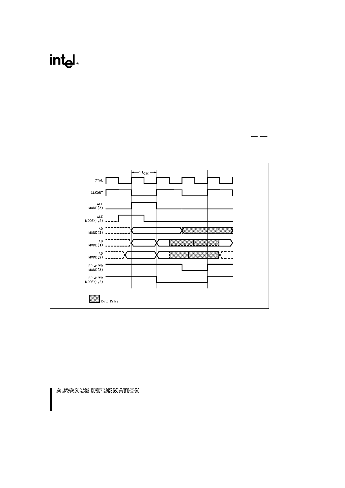
8XC196NT ADDITIONAL BUS TIMING MODES
The 8XC196NT device has 3 additional bus timing
modes for external memory interfacing.
MODE 3:
Mode 3 is the standard timing mode. Use this mode
for systems that emulate the 8XC196KR bus timings.
MODE 0:
Mode 0 is the standard timing mode, but 1 (minimum) wait state is always inserted in external bus
cycles.
MODE 1:
Mode 1 is the long R/W mode. This mode advances
RD
and WR signals by 1 T
OSC
creatinga2T
OSC
RD/WR low time. ALE is also advanced by 0.5 T
OSC
but ALE high time remains 1 T
OSC
.
MODE 2:
Mode 2 is the long R/W mode with Early Address.
Mode 2 is similar to Mode 1 with respect to RD
,WR,
and ALE signals. Additionally, the address is output
on the bus 0.5 T
OSC
earlier in the bus cycle.
272267– 4
Figure 4. Detailed MODE 1, 2, 3, Comparison
9
8XC196NT
EXPLANATION OF AC SYMBOLS
Each symbol is two pairs of letters prefixed by ‘‘T’’
for time. The characters in a pair indicate a signal
and its condition, respectively. Symbols represent
the time between the two signal/condition points.
Conditions: Signals:
HÐHigh AÐAddress HAÐHLDA
LÐLow BÐBHE LÐALE/ADV
VÐValid BRÐBREQ QÐData Out
XÐNo Longer CÐCLKOUT RDÐRD
Valid DÐDATA WÐWR/WRH/WRI
ZÐFloating GÐBuswidth XÐXTAL1
HÐHOLD
YÐREADY
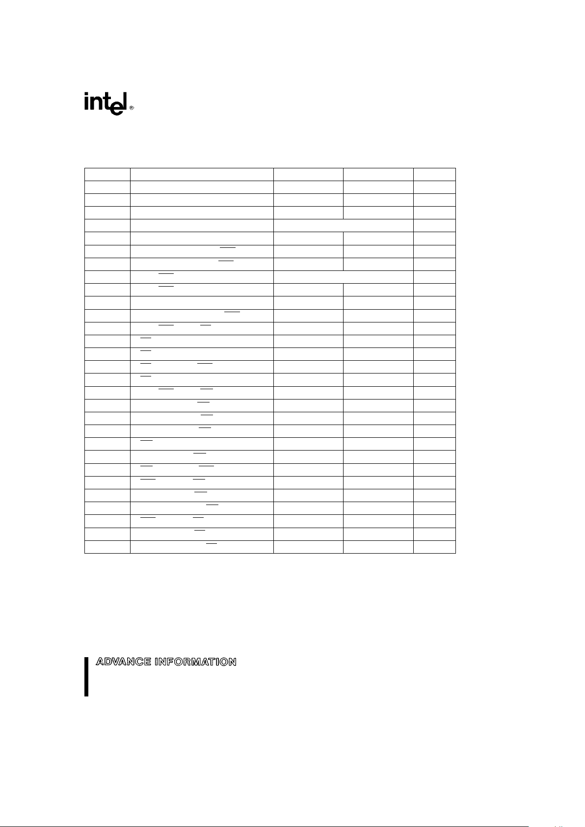
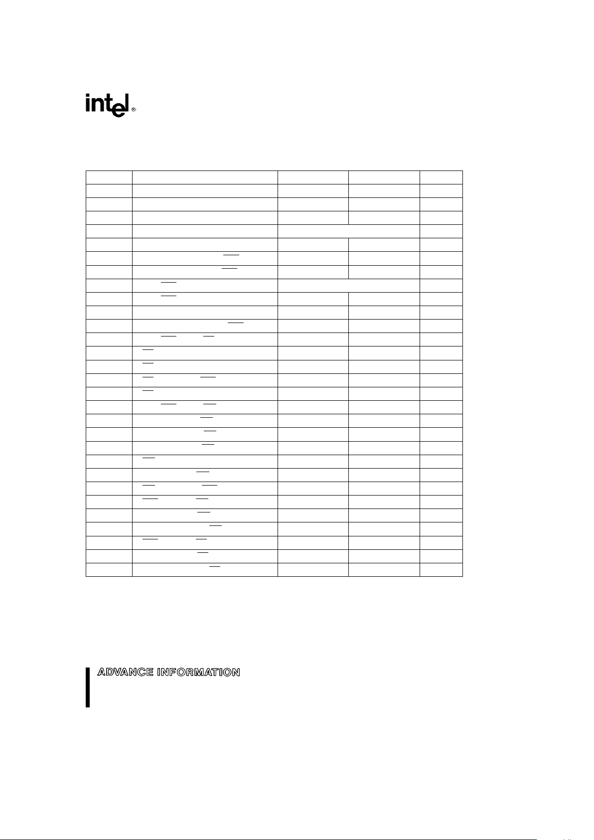
BUS MODE 0 and 3ÐAC CHARACTERISTICS (Over Specified Operating Conditions)
Test Conditions: Capacitance Load on All Pins
e
100 pF, Rise and Fall Timese10 ns.
The system must meet these specifications to work with the 8XC196NT.
Symbol Parameter Min Max Units
T
AVYV
Address Valid to Ready Setup 2 T
OSC
b
75 ns
(3)
T
YLYH
Non READY Time No Upper Limit ns
T
CLYX
READY Hold after CLKOUT Low 0 T
OSC
b
30 ns
(1)
T
AVGV
Address Valid to BUSWIDTH Setup 2 T
OSC
b
75 ns
(2, 3)
T
LLGV
ALE Low to BUSWIDTH Setup T
OSC
b
60 ns
(2, 3)
T
CLGX
BUSWIDTH Hold after CLKOUT Low 0 ns
T
AVDV
Address Valid to Input Data Valid 3 T
OSC
b
55 ns
(2)
T
RLDV
RD active to input Data Valid T
OSC
b
30 ns
(2)
T
CLDV
CLKOUT Low to Input Data Valid T
OSC
b
60 ns
T
RHDZ
End of RD to Input Data Float T
OSC
ns
T
RHDX
Data Hold after RD High 0 ns
NOTES:
1. If Max is exceeded, additional wait states will occur.
2. If wait states are used, add 2 T
OSC
c
n, where nenumber of wait states.
3. If mode 0 is selected, one wait state minimum is always added. If additional wait states are required, add 2 T
OSC
to the
specification.
10
8XC196NT
BUS MODE 0 and 3ÐAC CHARACTERISTICS (Over Specified Operating Conditions)
Test Conditions: Capacitance Load on All Pins
e
100 pF, Rise and Fall Timese10 ns.
The 8XC196NT will meet these specifications
Symbol Parameter Min Max Units
F
XTAL
Frequency on XTAL1 4.0 20 MHz
(1)
T
OSC
XTAL1 Period (1/F
XTAL
) 50 250 ns
T
XHCH
XTAL1 High to CLKOUT High or Low
a
20 110 ns
T
OFD
Clock Failure to Reset Pulled Low
(6)
440ms
T
CLCL
CLKOUT Period 2 T
OSC
ns
T
CHCL
CLKOUT High Period T
OSC
b
10 T
OSC
a
30 ns
T
CLLH
CLKOUT Low to ALE/ADV High
b
10
a
15 ns
T
LLCH
ALE/ADV Low to CLKOUT High
b
25
a
15 ns
T
LHLH
ALE/ADV Cycle Time 4 T
OSC
ns
(5)
T
LHLL
ALE/ADV High Time T
OSC
b
10 T
OSC
a
10 ns
T
AVLL
Address Valid to ALE Low T
OSC
b
15 ns
T
LLAX
Address Hold After ALE/ADV Low T
OSC
b
40 ns
T
LLRL
ALE/ADV Low to RD Low T
OSC
b
40 ns
T
RLCL
RD Low to CLKOUT Low
b
5
a
35 ns
T
RLRH
RD Low Period T
OSC
b
5ns
(5)
T
RHLH
RD High to ALE/ADV High T
OSC
T
OSC
a
25 ns
(3)
T
RLAZ
RD Low to Address Float
a
5ns
T
LLWL
ALE/ADV Low to WR Low T
OSC
b
10 ns
T
CLWL
CLKOUT Low to WR Low
b
10
a
25 ns
T
QVWH
Data Valid before WR High T
OSC
b
23 ns
T
CHWH
CLKOUT High to WR High
b
10
a
15 ns
T
WLWH
WR Low Period T
OSC
b
30 ns
(5)
T
WHQX
Data Hold after WR High T
OSC
b
35 ns
T
WHLH
WR High to ALE/ADV High T
OSC
b
10 T
OSC
a
15 ns
(3)
T
WHBX
BHE, INST Hold after WR High T
OSC
b
10 ns
T
WHAX
AD8– 15 Hold after WR High T
OSC
b
30 ns
(4)
T
RHBX
BHE, INST Hold after RD High T
OSC
b
10 ns
T
RHAX
AD8– 15 Hold after RD High T
OSC
b
30 ns
(4)
NOTES:
1. Testing performed at 8.0 MHz, however, the device is static by design and will typically operate below 1 Hz.
2. Typical specifications, not guaranteed.
3. Assuming back-to-back bus cycles.
4. 8-bit bus only.
5. If wait states are used, add 2 T
OSC
c
n, where nenumber of wait states. If mode 0 (1 automatic wait state added)
operation is selected, add 2 T
OSC
to specification.
6. T
OFD
is the time for the oscillator fail detect circuit (OFD) to react to a clock failure. The OFD circuitry is enabled by
programming the UPROM location 0778H with the value 0004H. NT/NQ customer QROM codes need to equate location
2016H to the value 0CDEH if the oscillator fail detect (OFD) function is desired. Intel manufacturing uses location 2016H
as a flag to determine whether or not to program the Clock Detect Enable (CDE) bit. Programming the CDE bit
enables oscillator fail detection.
11
8XC196NT
BUS MODE 0 and 3Ð8XC196NT SYSTEM BUS TIMING
272267– 5
*If mode 0 operation is selected, add 2 T
OSC
to this time.
12
8XC196NT
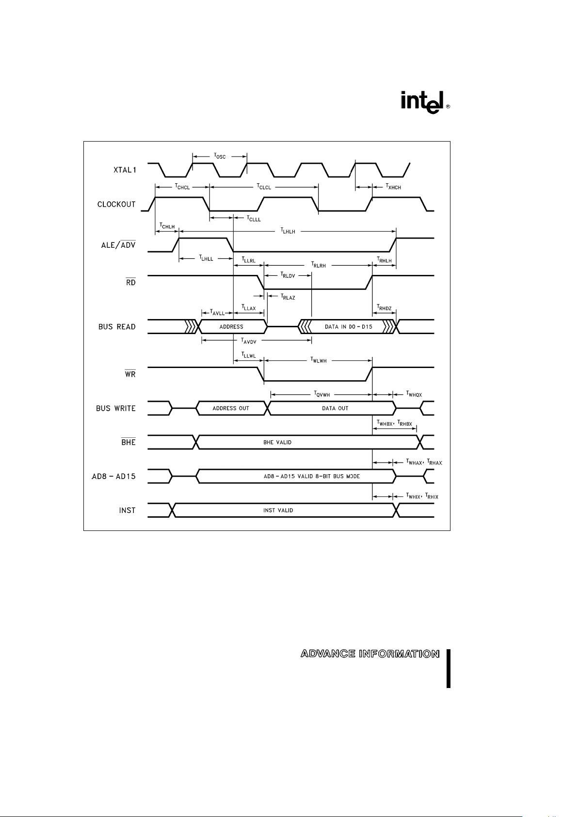
8XC196NT MODE 0 and 3ÐREADY TIMINGS (ONE WAIT STATE)
272267– 6
*If mode 0 selected, one wait state is always added. If additional wait states are required, add 2 T
OSC
to these specifica-
tions.
MODE 0 and 3Ð8XC196NT BUSWIDTH TIMINGS
272267– 7
*If mode 0 selected, add 2 T
OSC
to these specifications.
13

8XC196NT
BUS MODE 1ÐAC CHARACTERISTICS (Over Specified Operating Conditions)
Test Conditions: Capacitance Load on All Pins
e
100 pF, Rise and Fall Timese10 ns.
The system must meet these specifications to work with the 8XC196NT.
Symbol Parameter Min Max Units
T
AVYV
Address Valid to Ready Setup 2 T
OSC
b
75 ns
T
YLYH
Non READY Time No Upper Limit ns
T
CLYX
READY Hold after CLKOUT Low 0 T
OSC
b
30 ns
(1)
T
AVGV
Address Valid to BUSWIDTH Setup 2 T
OSC
b
75 ns
T
LLGV
ALE Low to BUSWIDTH Setup 1.5 T
OSC
b
60 ns
T
CLGX
BUSWIDTH Hold after CLKOUT Low 0 ns
T
AVDV
Address Valid to Input Data Valid 3 T
OSC
b
60 ns
(2)
T
RLDV
RD active to input Data Valid 2 T
OSC
b
44 ns
(2)
T
CLDV
CLKOUT Low to Input Data Valid T
OSC
b
60 ns
T
RHDZ
End of RD to Input Data Float T
OSC
ns
T
RHDX
Data Hold after RD High 0 ns
NOTES:
1. If Max is exceeded, additional wait states will occur.
2. If wait states are used, add 2 T
OSC
c
n, where nenumber of wait states.
14
8XC196NT
BUS MODE 1ÐAC CHARACTERISTICS (Over Specified Operating Conditions)
Test Conditions: Capacitance Load on All Pins
e
100 pF, Rise and Fall Timese10 ns.
The 8XC196NT will meet these specifications
Symbol Parameter Min Max Units
F
XTAL
Frequency on XTAL1 8.0 20 MHz
(1)
T
OSC
XTAL1 Period (1/F
XTAL
) 50 125 ns
T
XHCH
XTAL1 High to CLKOUT High or Low
a
20 110 ns
T
CLCL
CLKOUT Period 2 T
OSC
ns
T
CHCL
CLKOUT High Period T
OSC
b
10 T
OSC
a
27 ns
T
CHLH
CLKOUT HIGH to ALE/ADV High 0.5 T
OSC
b
15 0.5 T
OSC
a
15 ns
T
CLLL
CLKOUT LOW to ALE/ADV Low 0.5 T
OSC
b
25 0.5 T
OSC
a
15 ns
T
LHLH
ALE/ADV Cycle Time 4 T
OSC
ns
(5)
T
LHLL
ALE/ADV High Time T
OSC
b
20 T
OSC
a
10 ns
T
AVLL
Address Valid to ALE Low 0.5 T
OSC
b
20 ns
T
LLAX
Address Hold After ALE/ADV Low 0.5 T
OSC
b
25 ns
T
LLRL
ALE/ADV Low to RD Low 0.5 T
OSC
b
15 ns
T
RLCL
RD Low to CLKOUT Low T
OSC
b
10 T
OSC
a
30 ns
T
RLRH
RD Low Period 2 T
OSC
b
20 ns
(5)
T
RHLH
RD High to ALE/ADV High 0.5 T
OSC
0.5 T
OSC
a
25 ns
(3)
T
RLAZ
RD Low to Address Float
a
5ns
T
LLWL
ALE/ADV Low to WR Low 0.5 T
OSC
b
10 ns
T
CLWL
CLKOUT Low to WR Low T
OSC
b
15 T
OSC
a
25 ns
T
QVWH
Data Valid before WR High 2 T
OSC
b
23 ns
T
CHWH
CLKOUT High to WR High
b
10
a
15 ns
T
WLWH
WR Low Period 2 T
OSC
b
15 ns
(5)
T
WHQX
Data Hold after WR High 0.5 T
OSC
b
12 ns
T
WHLH
WR High to ALE/ADV
High 0.5 T
OSC
b
10 0.5 T
OSC
a
15 ns
(3)
T
WHBX
BHE Hold after WR High T
OSC
b
15 ns
T
WHIX
INST Hold after WR High 0.5 T
OSC
b
15
T
WHAX
AD8– 15 Hold after WR High 0.5 T
OSC
b
30 ns
(4)
T
RHBX
BHE Hold after RD High T
OSC
b
32 ns
T
RHIX
INST Hold after RD High 0.5 T
OSC
b
32
T
RHAX
AD8– 15 Hold after RD High 0.5 T
OSC
b
30 ns
(4)
NOTES:
1. Testing performed at 8.0 MHz, however, the device is static by design and will typically operate below 1 Hz.
2. Typical specifications, not guaranteed.
3. Assuming back-to-back bus cycles.
4. 8-bit bus only.
5. If wait states are used, add 2 T
OSC
c
n, where nenumber of wait states.
15
8XC196NT
MODE 1Ð8XC196NT SYSTEM BUS TIMING
272267– 8
16
8XC196NT
MODE 1Ð8XC196NT READY TIMINGS (ONE WAIT STATE)
272267– 9
MODE 1Ð8XC196NT BUSWIDTH TIMINGS
272267– 10
17
8XC196NT
BUS MODE 2ÐAC CHARACTERISTICS (Over Specified Operating Conditions)
Test Conditions: Capacitance Load on All Pins
e
100 pF, Rise and Fall Timese10 ns.
The system must meet these specifications to work with the 8XC196NT.
Symbol Parameter Min Max Units
T
AVYV
Address Valid to Ready Setup 2.5 T
OSC
b
75 ns
T
YLYH
Non READY Time No Upper Limit ns
T
CLYX
READY Hold after CLKOUT Low 0 T
OSC
b
30 ns
(1)
T
AVGV
Address Valid to BUSWIDTH Setup 2.5 T
OSC
b
75 ns
T
LLGV
ALE Low to BUSWIDTH Setup 1.5 T
OSC
b
60 ns
T
CLGX
BUSWIDTH Hold after CLKOUT Low 0 ns
T
AVDV
Address Valid to Input Data Valid 3.5 T
OSC
b
55 ns
(2)
T
RLDV
RD active to input Data Valid 2 T
OSC
b
44 ns
(2)
T
CLDV
CLKOUT Low to Input Data Valid T
OSC
b
60 ns
T
RHDZ
End of RD to Input Data Float 0.5 T
OSC
ns
T
RHDX
Data Hold after RD High 0 ns
NOTES:
1. If Max is exceeded, additional wait states will occur.
2. If wait states are used, add 2 T
OSC
c
n, where nenumber of wait states.
18
8XC196NT
BUS MODE 2ÐAC CHARACTERISTICS (Over Specified Operating Conditions)
Test Conditions: Capacitance Load on All Pins
e
100 pF, Rise and Fall Timese10 ns.
The 8XC196NT will meet these specifications
Symbol Parameter Min Max Units
F
XTAL
Frequency on XTAL1 8.0 20 MHz
(1)
T
OSC
XTAL1 Period (1/F
XTAL
) 50 125 ns
T
XHCH
XTAL1 High to CLKOUT High or Low
a
20
a
85 ns
T
CLCL
CLKOUT Period 2 T
OSC
ns
T
CHCL
CLKOUT High Period T
OSC
b
10 T
OSC
a
27 ns
T
CHLH
CLKOUT HIGH to ALE/ADV High 0.5 T
OSC
b
15 0.5 T
OSC
a
15 ns
T
CLLL
CLKOUT LOW to ALE/ADV Low 0.5 T
OSC
b
25 0.5 T
OSC
a
15 ns
T
LHLH
ALE/ADV Cycle Time 4 T
OSC
ns
(5)
T
LHLL
ALE/ADV High Time T
OSC
b
20 T
OSC
a
10 ns
T
AVLL
Address Valid to ALE Low T
OSC
b
15 ns
T
LLAX
Address Hold After ALE/ADV Low 0.5 T
OSC
b
20 ns
T
LLRL
ALE/ADV Low to RD Low 0.5 T
OSC
b
15 ns
T
RLCL
RD Low to CLKOUT Low T
OSC
b
10 T
OSC
a
30 ns
T
RLRH
RD Low Period 2 T
OSC
b
20 ns
(5)
T
RHLH
RD High to ALE/ADV High 0.5 T
OSC
b
5 0.5 T
OSC
a
25 ns
(3)
T
RLAZ
RD Low to Address Float
a
5ns
T
LLWL
ALE/ADV Low to WR Low 0.5 T
OSC
b
10 ns
T
CLWL
CLKOUT Low to WR Low T
OSC
b
22 T
OSC
a
25 ns
T
QVWH
Data Valid before WR High 2 T
OSC
b
25 ns
T
CHWH
CLKOUT High to WR High
b
10
a
15 ns
T
WLWH
WR Low Period 2 T
OSC
b
20 ns
(5)
T
WHQX
Data Hold after WR High 0.5 T
OSC
b
12 ns
T
WHLH
WR High to ALE/ADV High 0.5 T
OSC
b
10 0.5 T
OSC
a
10 ns
(3)
T
WHBX
BHE Hold after WR High T
OSC
b
15 ns
T
WHIX
INST Hold after WR High 0.5 T
OSC
b
15
T
WHAX
AD8– 15 Hold after WR High 0.5 T
OSC
b
30 ns
(4)
T
RHBX
BHE Hold after RD High T
OSC
b
32 ns
T
RHIX
INST Hold after RD High 0.5 T
OSC
b
32
T
RHAX
AD8– 15 Hold after RD High 0.5 T
OSC
b
30 ns
(4)
NOTES:
1. Testing performed at 8.0 MHz, however, the device is static by design and will typically operate below 1 Hz.
2. Typical specifications, not guaranteed.
3. Assuming back-to-back bus cycles.
4. 8-bit bus only.
5. If wait states are used, add 2 T
OSC
c
n, where nenumber of wait states.
19
8XC196NT
MODE 2Ð8XC196NT SYSTEM BUS TIMING
272267– 11
20

8XC196NT
MODE 2Ð8XC196NT READY TIMINGS (ONE WAIT STATE)
272267– 12
MODE 2Ð8XC196NT BUSWIDTH TIMINGS
272267– 13
21
8XC196NT
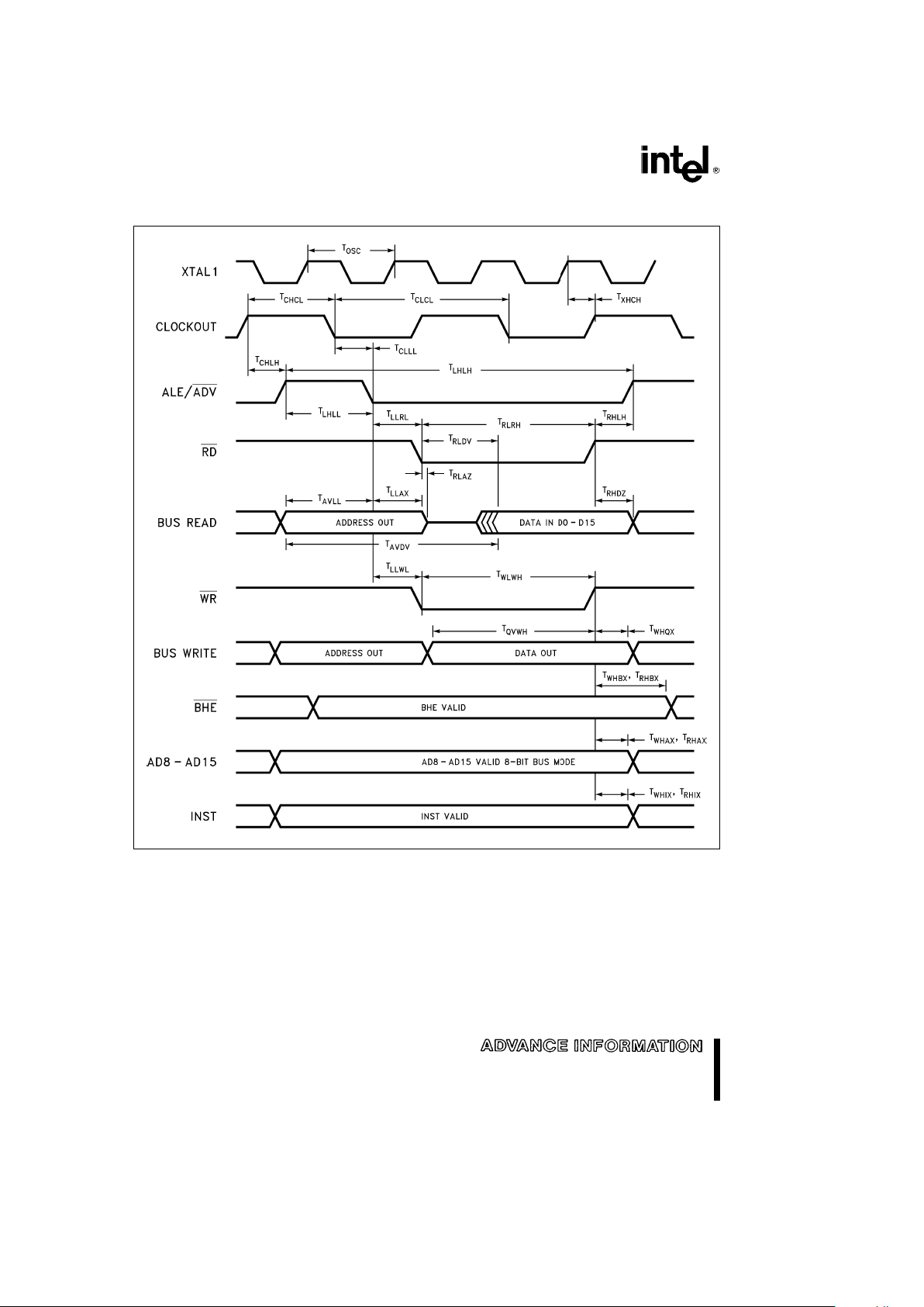
BUS MODE 0, 1, 2, and 3ÐHOLD/HLDA TIMINGS (Over Specified Operation Conditions)
Test Conditions: Capacitance Load on All Pins
e
100 pF, Rise and Fall Timese10 ns.
Symbol Parameter Min Max Units
T
HVCH
HOLD Setup Time
a
65 ns
(1)
T
CLHAL
CLKOUT Low to HLDA Low
b
15
a
15 ns
T
CLBRL
CLKOUT Low to BREQ Low
b
15
a
15 ns
T
HALAZ
HLDA Low to Address Float
a
25 ns
T
HALBZ
HLDA Low to BHE, INST, RD,WRWeakly Driven
a
25 ns
T
CLHAH
CLKOUT Low to HLDA High
b
25
a
15 ns
T
CLBRH
CLKOUT Low to BREQ High
b
25
a
25 ns
T
HAHAX
HLDA High to Address No Longer Float
b
15 ns
T
HAHBV
HLDA High to BHE, INST, RD,WRValid
b
10 ns
NOTE:
1. To guarantee recognition at next clock.
8XC196NT HOLD/HLDA TIMINGS
272267– 14
22
8XC196NT
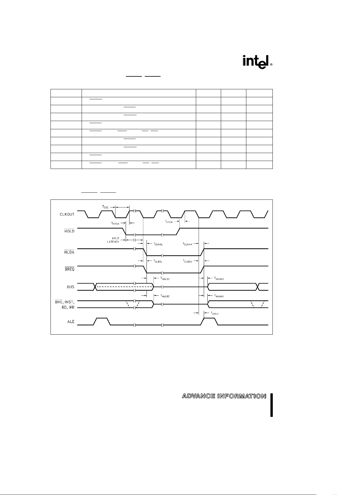
AC CHARACTERISTICSÐSLAVE PORT
SLAVE PORT WAVEFORMÐ(SLPLe0)
272267– 15
SLAVE PORT TIMINGÐ(SLPLe0)
Symbol Parameter Min Max Units
T
SAVWL
Address Valid to WR Low 50 ns
T
SRHAV
RD High to Address Valid 60 ns
T
SRLRH
RD Low Period T
OSC
ns
T
SWLWH
WR Low Period T
OSC
ns
T
SRLDV
RD Low to Output Data Valid 60 ns
T
SDVWH
Input Data Setup to WR High 20 ns
T
SWHQX
WR High to Data Invalid 30 ns
T
SRHDZ
RD High to Data Float 15 ns
NOTES:
1. Test Conditions: F
OSC
e
20 MHz, T
OSC
e
50 ns. Rise/Fall Timee10 ns. Capacitive Pin Loade100 pF.
2. These values are not tested in production, and are based upon theoretical estimates and/or laboratory tests.
3. Specifications above are advanced information and are subject to change.
23
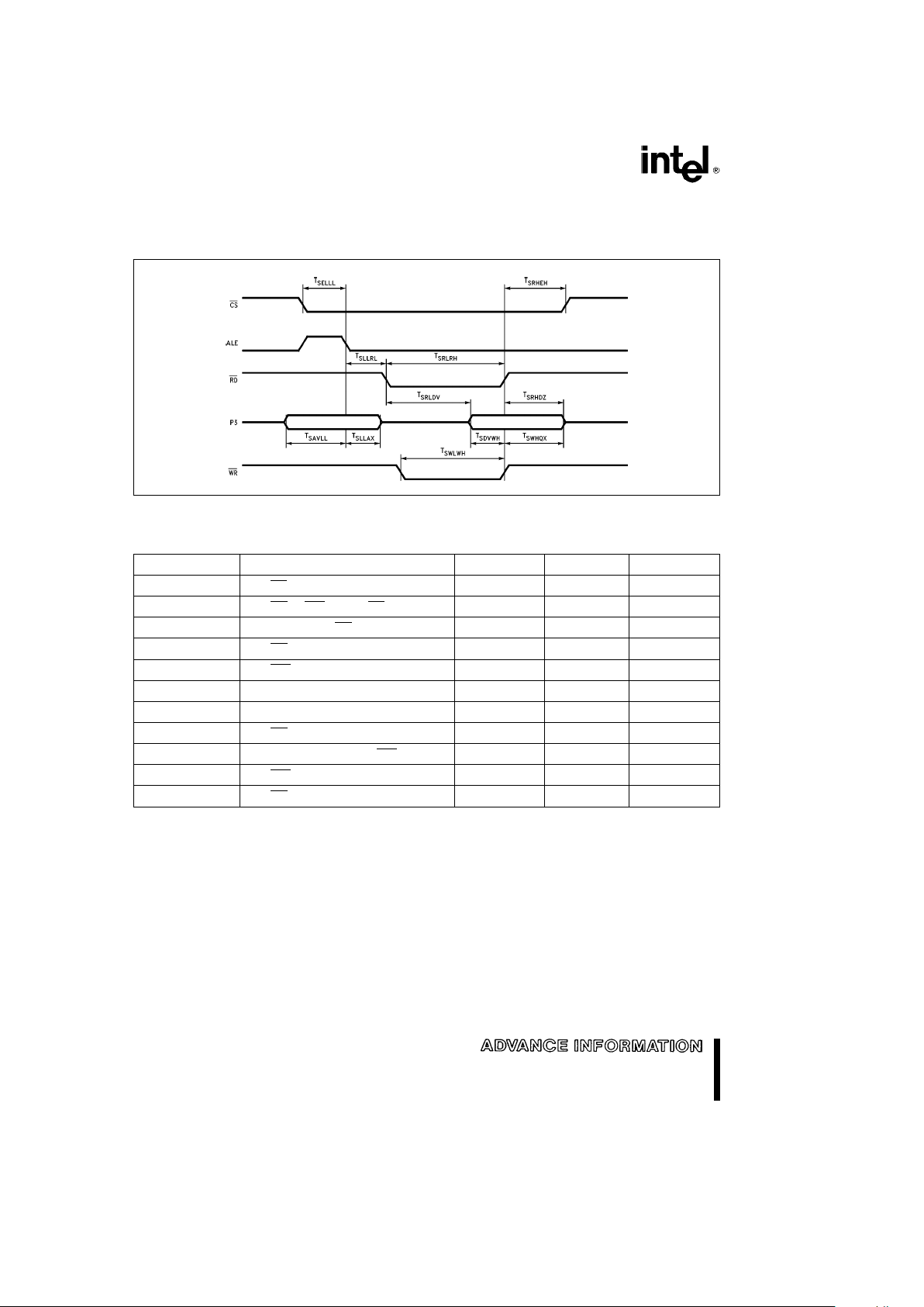
8XC196NT
AC CHARACTERISTICSÐSLAVE PORT (Continued)
SLAVE PORT WAVEFORMÐ(SLPL
e
1)
272267– 16
SLAVE PORT TIMINGÐ(SLPLe1)
Symbol Parameter Min Max Units
T
SELLL
CS Low to ALE Low 20 ns
T
SRHEH
RD or WR High to CS High 60 ns
T
SLLRL
ALE Low to RD Low T
OSC
ns
T
SRLRH
RD Low Period T
OSC
ns
T
SWLWH
WR Low Period T
OSC
ns
T
SAVLL
Address Valid to ALE Low 20 ns
T
SLLAX
ALE Low to Address Invalid 20 ns
T
SRLDV
RD Low to Output Data Valid 60 ns
T
SDVWH
Input Data Setup to WR High 20 ns
T
SWHQX
WR High to Data Invalid 30 ns
T
SRHDZ
RD High to Data Float 15 ns
NOTES:
1. Test Conditions: F
OSC
e
20 MHz, T
OSC
e
50 ns. Rise/Fall Timee10 ns. Capacitive Pin Loade100 pF.
2. These values are not tested in production, and are based upon theoretical estimates and/or laboratory tests.
3. Specifications above are advanced information and are subject to change.
24
8XC196NT
EXTERNAL CLOCK DRIVE
Symbol Parameter Min Max Units
1/T
XLXL
Oscillator Frequency 4 20 MHz
T
XLXL
Oscillator Period (T
OSC
) 50 250 ns
T
XHXX
High Time 0.35cT
OSC
0.65 T
OSC
ns
T
XLXX
Low Time 0.35cT
OSC
0.65 T
OSC
ns
T
XLXH
Rise Time 10 ns
T
XHXL
Fall Time 10 ns
EXTERNAL CLOCK DRIVE WAVEFORMS
272267– 17
AC TESTING INPUT, OUTPUT WAVEFORMS
272267– 18
AC Testing inputs are driven at 3.5V for a logic ‘‘1’’ and
0.45V for a logic ‘‘0’’. Timing measurements are made
at 2.0V for a logic ‘‘1’’ and 0.8V for logic ‘‘0’’.
FLOAT WAVEFORMS
272267– 19
For timing purposes a Port Pin is no longer floating
when a 150 mV change from load voltage occurs and
begins to float when a 150 mV change from the loading
V
OH/VOL
level occurs IOL/I
OH
s
15 mA.
25
8XC196NT
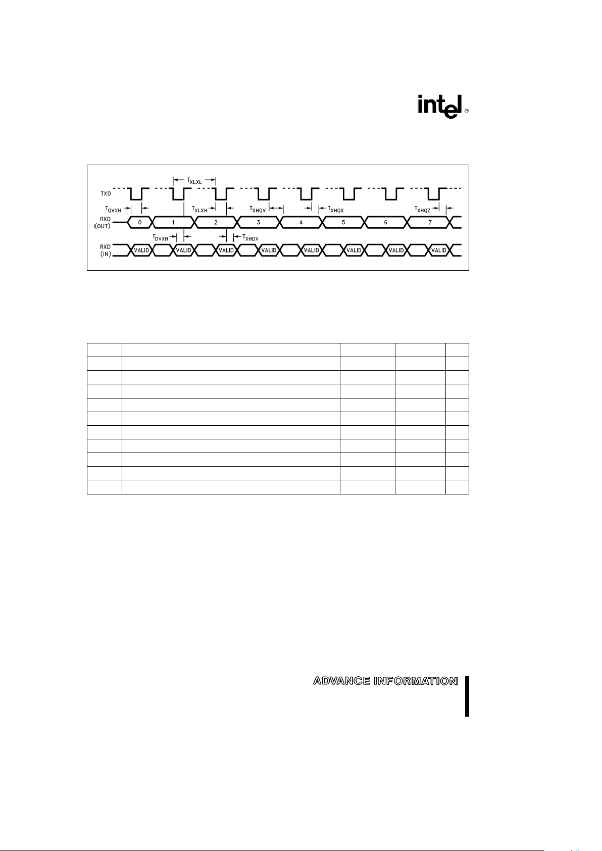
WAVEFORMÐSERIAL PORTÐSHIFT REGISTER MODE
SERIAL PORT WAVEFORMÐSHIFT REGISTER MODE (MODE 0)
272267– 20
AC CHARACTERISTICSÐSERIAL PORT-SHIFT REGISTER MODE
SERIAL PORT TIMINGÐSHIFT REGISTER MODE (MODE 0)
Test Conditions: T
A
eb
40§Ctoa125§C; V
CC
e
5.0Vg10%; V
SS
e
0.0V; Load CapacitanceepF
Symbol Parameter Min Max Units
T
XLXL
(2)
Serial Port Clock Period (BRRt8002H) Receive Only 6 T
OSC
ns
T
XLXH
(2)
Serial Port Clock Falling Edge to Rising Edge (BRRt8002H) 4 T
OSC
b
50 4 T
OSC
a
50 ns
T
XLXL
(2)
Serial Port Clock Period (BRRe8001H) Transmit Only 4 T
OSC
ns
T
XLXH
(2)
Serial Port Clock Falling Edge to Rising Edge (BRRe8001H) 2 T
OSC
b
50 2 T
OSC
a
50 ns
T
QVXH
Output Data Setup to Clock Rising Edge 3 T
OSC
ns
T
XHQX
Output Data Hold after Clock Rising Edge 2 T
OSC
b
50 ns
T
XHQV
Next Output Data Valid after Clock Rising Edge 2 T
OSC
a
50 ns
T
DVXH
Input Data Setup to Clock Rising Edge 2 T
OSC
a
200 ns
T
XHDX
(1)
Input Data Hold after Clock Rising Edge 0 ns
T
XHQZ
(1)
Last Clock Rising to Output Float 5 T
OSC
ns
NOTES:
1. Parameters not tested.
2. The minimum baud rate register value for Receive is 8002H. The minimum baud rate register value for Transmit is 8001H.
26
8XC196NT
A to D CHARACTERISTICS
The A/D converter is ratiometric, so absolute accuracy is dependent on the accuracy and stability of V
REF
.
10-BIT MODE A/D OPERATING CONDITIONS
Symbol Description Min Max Units
T
A
Ambient Temperature 0
a
70
§
C
V
CC
Digital Supply Voltage 4.50 5.50 V
V
REF
Analog Supply Voltage 4.50 5.50 V
(1)
T
SAM
Sample Time 1.0 ms
(2)
T
CONV
Conversion Time 10 15 ms
(2)
F
OSC
Oscillator Frequency 4.0 20 MHz
NOTES:
1. V
REF
must be within 0.5V of VCC.
2. The value of ADÐTIME is selected to meet these specifications.
10-BIT MODE A/D CHARACTERISTICS (Using Above Operating Conditions)
(6)
Parameter Typ*
(1)
Min Max Units*
Resolution
1024 1024 Level
10 10 Bits
Absolute Error 0
g
3.0 LSBs
Full Scale Error 0.25g0.5 LSBs
Zero Offset Error 0.25g0.5 LSBs
Non-Linearity 1.0g2.0
g
3.0 LSBs
Differential Non-Linearity
b
0.75
a
0.75 LSBs
Channel-to-Channel Matching
g
0.1 0
g
1.0 LSBs
Repeatability
g
0.25 0 LSBs
(1)
Temperature Coefficients:
Offset 0.009 LSB/C
(1)
Full Scale 0.009 LSB/C
(1)
Differential Non-Linearity 0.009 LSB/C
(1)
Off Isolation
b
60 dB
(1,2,3)
Feedthrough
b
60 dB
(1,2)
VCCPower Supply Rejection
b
60 dB
(1,2)
Input Resistance 750 1.2K X
(4)
DC Input Leakage
g
1.0 0
g
3.0 mA
Voltage on Analog Input Pin ANGNDb0.5 V
REF
a
0.5 V
(5)
Sampling Capacitor 3.0 pF
*An ‘‘LSB’’ as used here has a value of approximately 5 mV.
NOTES:
1. These values are expected for most parts at 25
§
C, but are not tested or guaranteed.
2. DC to 100 KHz.
3. Multiplexer break-before-make is guaranteed.
4. Resistance from device pin, through internal MUX, to sample capacitor.
5. Applying voltages beyond these specifications will degrade the accuracy of other channels being converted.
6. All conversions performed with processor in IDLE mode.
27
8XC196NT
8-BIT MODE A/D OPERATING CONDITIONS
Symbol Description Min Max Units
T
A
Ambient Temperature 0
a
70
§
C
V
CC
Digital Supply Voltage 4.50 5.50 V
V
REF
Analog Supply Voltage 4.50 5.50 V
(1)
T
SAM
Sample Time 1.0 ms
(2)
T
CONV
Conversion Time 7 20 ms
(2)
F
OSC
Oscillator Frequency 4.0 20 MHz
NOTES:
1. V
REF
must be within 0.5V of VCC.
2. The value of ADÐTIME is selected to meet these specifications.
8-BIT MODE A/D CHARACTERISTICS (Using Above Operating Conditions)
(6)
Parameter Typ*
(1)
Min Max Units*
Resolution
256 256 Level
8 8 Bits
Absolute Error 0
g
1.0 LSBs
Full Scale Error
g
0.5 LSBs
Zero Offset Error
g
0.5 LSBs
Non-Linearity 0
g
1.0 LSBs
Differential Non-Linearity
b
0.5
a
0.5 LSBs
Channel-to-Channel Matching 0
g
1.0 LSBs
Repeatability
g
0.25 0 LSBs
(1)
Temperature Coefficients:
Offset 0.003 LSB/C
(1)
Full Scale 0.003 LSB/C
(1)
Differential Non-Linearity 0.003 LSB/C
(1)
Off Isolation
b
60 dB
(1,2,3)
Feedthrough
b
60 dB
(1,2)
VCCPower Supply Rejection
b
60 dB
(1,2)
Input Resistance 750 1.2K X
(4)
DC Input Leakage
g
1.0 0
g
3.0 mA
Voltage on Analog Input Pin ANGNDb0.5 V
REF
a
0.5 V
(5)
Sampling Capacitor 3.0 pF
*An ‘‘LSB’’ as used here has a value of approximately 5 mV.
NOTES:
1. These values are expected for most parts at 25
§
C, but are not tested or guaranteed.
2. DC to 100 KHz.
3. Multiplexer break-before-make is guaranteed.
4. Resistance from device pin, through internal MUX, to sample capacitor.
5. Applying voltage beyond these specifications will degrade the accuracy of other channels being converted.
6. All conversions performed with processor in IDLE mode.
28
8XC196NT
OTPROM SPECIFICATIONS
OPERATING CONDITIONS
Symbol Description Min Max Units
T
A
Ambient Temperature During Programming 20 30
§
C
V
CC
Supply Voltage During Programming 4.5 5.5 V
(1)
V
REF
Reference Supply Voltage During Programming 4.5 5.5 V
(1)
V
PP
Programming Voltage 12.25 12.75 V
(2)
V
EA
EA Pin Voltage 12.25 12.75 V
(2)
F
OSC
Oscillator Frequency during Auto 6.0 8.0 MHz
and Slave Mode Programming
F
OSC
Oscillator Frequency during 6.0 20.0 MHz
Run-Time Programming
NOTES:
1. V
CC
and V
REF
should nominally be at the same voltage during programming.
2. V
PP
and VEAmust never exceed the maximum specification, or the device may be damaged.
3. V
SS
and ANGND should nominally be at the same potential (0V).
4. Load capacitance during Auto and Slave Mode programming
e
150 pF.
AC OTPROM PROGRAMMING CHARACTERISTICS (SLAVE MODE)
Symbol Parameter Min Max Units
T
AVLL
Address Setup Time 0 T
OSC
T
LLAX
Address Hold Time 100 T
OSC
T
DVPL
Data Setup Time 0 T
OSC
T
PLDX
Data Hold Time 400 T
OSC
T
LLLH
PALE Pulse Width 50 T
OSC
T
PLPH
PROG Pulse Width
(2)
50 T
OSC
T
LHPL
PALE High to PROG Low 220 T
OSC
T
PHLL
PROG High to next PALE Low 220 T
OSC
T
PHDX
Word Dump Hold Time 50 T
OSC
T
PHPL
PROG High to next PROG Low 220 T
OSC
T
LHPL
PALE High to PROG Low 220 T
OSC
T
PLDV
PROG Low to Word Dump Valid 50 T
OSC
T
SHLL
RESET High to First PALE Low 1100 T
OSC
T
PHIL
PROG High to AINC Low 0 T
OSC
T
ILIH
AINC Pulse Width 240 T
OSC
T
ILVH
PVER Hold after AINC Low 50 T
OSC
T
ILPL
AINC Low to PROG Low 170 T
OSC
T
PHVL
PROG High to PVER Valid 220 T
OSC
NOTES:
1. Run-time programming is done with F
OSC
e
6.0 MHz to 10.0 MHz, VCC,VPD,V
REF
e
5Vg0.5V, T
C
e
25§Cg5§C and
V
PP
e
12.5Vg0.25V. For run-time programming over a full operating range, contact factory.
2. This specification is for the word dump mode. For programming pulses use Modified Quick Pulse Algorithm.
29
8XC196NT
DC OTPROM PROGRAMMING CHARACTERISTICS
Symbol Parameter Min Max Units
I
PP
VPPProgramming Supply Current 200 mA
NOTE:
Do not apply V
PP
unti VCCis stable and within specifications and the oscillator/clock has stabilized or the device may be
damaged.
OTPROM PROGRAMMING WAVEFORMS
SLAVE PROGRAMMING MODE DATA PROGRAM MODE WITH SINGLE PROGRAM PULSE
272267– 21
NOTE:
P3.0 must be high (‘‘1’’)
SLAVE PROGRAMMING MODE IN WORD DUMP MODE WITH AUTO INCREMENT
272267– 22
NOTE:
P3.0 must be low (‘‘0’’)
30
8XC196NT
SLAVE PROGRAMMING MODE TIMING IN DATA PROGRAM MODE WITH REPEATED PROG PULSE
AND AUTO INCREMENT
272267– 23
This data sheet (272267-004) applies to devices
marked with a ‘‘D’’ at the end of the top side tracking
number.
8XC196NT Design Considerations
1. When operating in bus timing modes 1 or 2, the
upper and lower address/data lines must be
latched. Even in 8-bit bus mode, the upper address lines must be latched. In modes 0 and 3,
the upper address lines DO NOT NEED to be
latched in 8-bit bus width mode. But in 16-bit
buswidth mode the upper address lines need to
be latched.
8XC196NT ERRATA see Faxback
Ý
2344
1. ILLEGAL Opcode interrupt vector.
2. Aborted Interrupt vectors to lowest priority.
3. PTS Request during Interrupt latency.
DATA SHEET REVISION HISTORY
This datasheet applies to devices marked with a ‘‘D’’
at the end of the topside tracking number. The topside tracking number consists of nine characters
and is the second line on the top side of the device.
Datasheets are changed as new device information
becomes available. Verify with your local Intel sales
office that you have the latest version before finalizing a design or ordering devices.
The following are differences between the 272267003 and 272267-004 datasheets:
1. Changed all references of ‘‘EPROM’’ to
‘‘OTPROM’’.
2. Added all the Slave Port pins to the package
diagram and pin descriptions.
3. Added INTOUT
pin to pin descriptions.
4. Changed ILI1 (input leakage current for Port 0)
from
g
1 mAtog3mA.
5. Removed T
LLYV
from AC characterisics and
waveform diagrams.
6. T
RLCL
in Mode 0 and 3, changed froma4ns
min. to
b
5 ns min.
7. T
WHQX
in Mode 0 and 3, changed from T
OSC
b
30 min. to T
OSC
b
35 min.
8. Clarified the Ready waveform timings for Mode
0 and 3, by adding ‘‘
a
2T
OSC
*’’.
9. T
LHLL
in Mode 1, changed from T
OSC
b
10 min.
to T
OSC
b
20 min.
10. T
AVLL
in Mode 1, changed from 0.5 T
OSC
b
15
min. to 0.5 T
OSC
b
20 min.
11. T
LLAX
in Mode 1, changed from 0.5 T
OSC
b
20
min. to 0.5 T
OSC
b
25 min.
12. T
LHLL
in Mode 2, changed from T
OSC
b
10 min.
to T
OSC
b
20 min.
13. T
XLXL
and T
XLXH
for the Serial Port timings
were changed to reflect the minimum baudrate
for receive and transmit modes.
14. Added the 8XC196NT ERRATA section.
31
 Loading...