

Page 1

74F841/842/843/845/846
Bus interface latches
Product specification
Replaces datasheet 74F841/842/843/844/845/846 of 1999 Jan 08
IC15 Data Handbook
1999 Jun 23
INTEGRATED CIRCUITS
Page 2
Philips Semiconductors Product specification
74F841/74F842/74F843/
74F845/74F846
Bus interface latches
74F841/74F842 10-bit bus interface latches, non-inverting/inverting (3-State)
74F843 9-bit bus interface latch, non-inverting (3-State)
74F845/74F846 8-bit bus interface latches, non-inverting/inverting (3-State)
2
1999 Jun 23 853–1208 21851
FEA TURES
•High speed parallel latches
•Extra data width for wide address/data paths or buses carrying
parity
•High impedance NPN base input structure minimizes bus loading
•IIL is 20µA vs 1000A for AM29841 series
•Buffered control inputs to reduce AC effects
•Ideal where high speed, light loading, or increased fan-in are
required as with MOS microprocessors
•Positive and negative over-shoots are clamped to ground
•3-State outputs glitch free during power-up and power-down
•48mA sink current
•Slim dual in-line 300 mil package
•Broadside pinout
•Pin-for-pin and function compatible with AMD AM29841-846
series
TYPE
TYPICAL
PROPAGATION
DELA Y
TYPICAL
SUPPLY CURRENT
(TOTAL)
74F841, 74F842 5.5ns 60mA
74F843, 74F845 5.5ns 75mA
74F846 6.2ns 60mA
DESCRIPTION
The 74F841–74F846 bus interface latch series are designed to
provide extra data width for wider address/data paths of buses
carrying parity.
The 74F841–74F846 series are funcitonally an pin compatible to the
AMD AM29841–AM29846 series.
The 74F841 consists of ten D-type latches with 3-State outputs. The
flip-flops appear transparent to the data when Latch Enable (LE) is
High. This allows asynchronous operation, as the output transition
follows the data in transition. On the LE High-to-Low transition, the
data that meets the setup and hold time is latched.
Data appears on the bus when the Output Enable (OE
) is Low.
When OE
is High the output is in the High-impedance state.
The 74F842 is the inverted output version of the 74F841.
The 74F843 consists of nine D-type latches with 3-State outputs. In
addition to the LE and OE
pins, the 74F843 has a Master Reset
(MR
) pin and Preset (PRE) pin. These pins are ideal for parity bus
interfacing in high performance systems. When MR
is Low, the
outputs are Low if OE
is Low. When MR is High, data can be
entered into the latch. When PRE
is Low, the outputs are High, if OE
is Low, PRE overrides MR.
The 74F845 consists of eight D-type latches with 3-State outputs. In
addition to the LE, OE
, MR and PRE pins, the 74F845 has two
addtitional OE
pins making a total of three Output Enables (OE0,
OE
1, OE2) pins.
The multiple Ouptut Enables (OE
0, OE1, OE2) allow multi-user
control of the interface, e.g., CS
, DMA, and RD/WR.
The 74F846 is the inverted output version of the 74F845.
ORDERING INFORMATION
PACKAGES
COMMERCIAL RANGE
VCC = 5V±10%; T
amb
= 0°C to +70°C
PACKAGE DRAWING
NUMBER
24-pin plastic Slim DIP (300 mil) N74F841N, N74F842N, N74F843N, N74F845N, N74F846N SOT222-1
24-pin plastic SOL N74F841D, N74F842D, N74F843D, N74F845D, N74F846D SOT137-1
INPUT AND OUTPUT LOADING AND FAN-OUT TABLE
PINS DESCRIPTION
74F(U.L.)
HIGH/LOW
LOAD VALUE
HIGH/LOW
Dn Data inputs 1.0/0.033 20µA/20µA
LE Latch Enable input 1.0/0.033 20µA/20µA
OE, OEn Output Enable input (active Low) 1.0/0.033 20µA/20µA
MR Master Reset input (active Low) 1.0/0.033 20µA/20µA
PRE Preset input (active Low) 1.0/0.033 20µA/20µA
Qn Data outputs 1200/80 24mA/48mA
Qn Data outputs 1200/80 24mA/48mA
NOTE: One (1.0) FAST Unit Load is defined as: 20µA in the High state and 0.6mA in the Low state.
Page 3

Philips Semiconductors Product specification
74F841/74F842/74F843/
74F845/74F846
Bus interface latches
1999 Jun 23
3
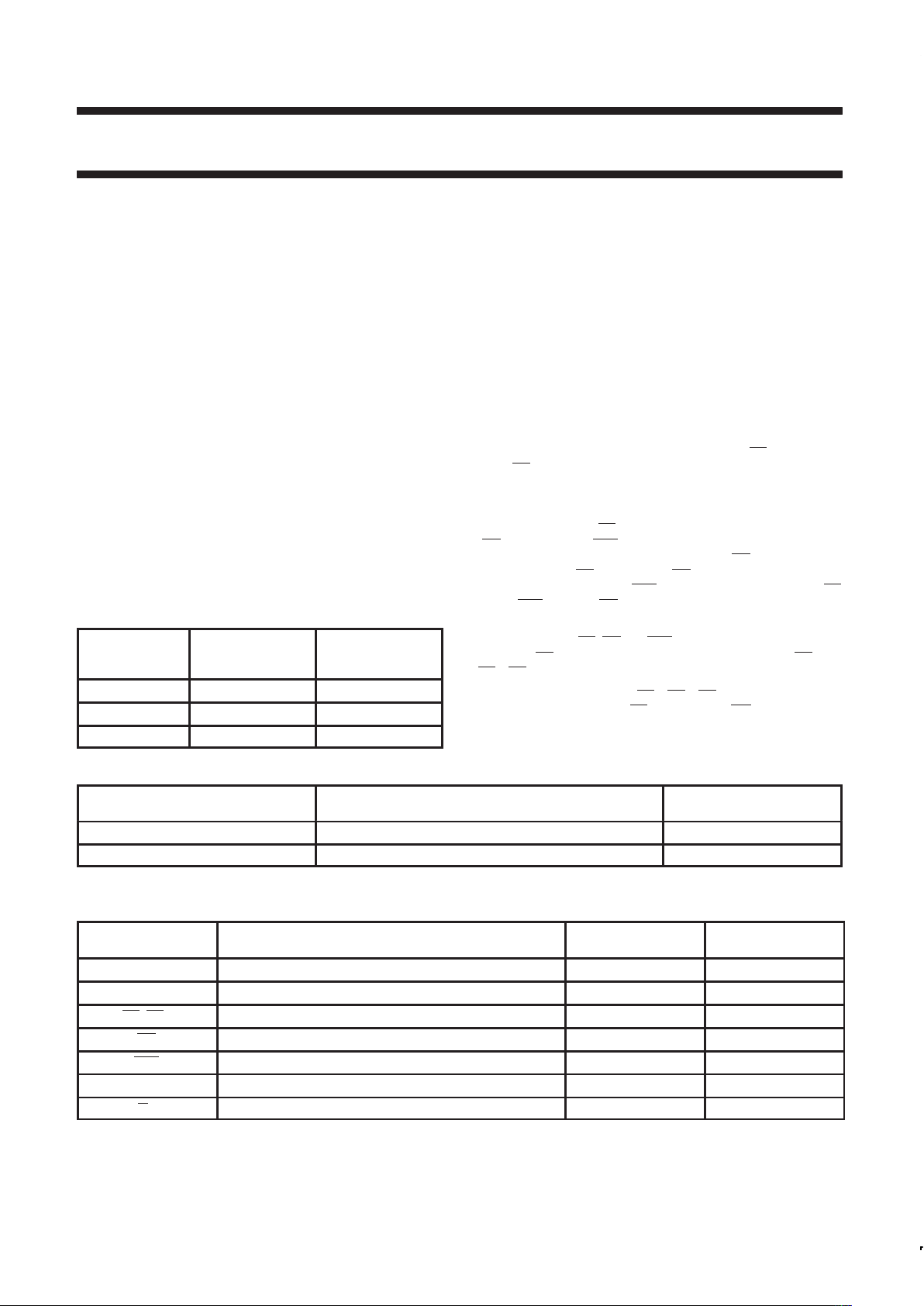
PIN CONFIGURATION for 74F841
1
2
3
4
5
6
7
8
9
10
11
12 13
14
15
16
17
18
19
20
21
22
23
24
OE
D0
D1
D2
D3
D4
D5
D6
D7
D8
D9
V
CC
Q0
Q1
Q2
Q3
Q4
Q5
Q7
Q6
Q8
Q9
LE
GND
SF01279
LOGIC SYMBOL for 74F841
13
2
SF01280
3456 78910
1
D0LED1 D2 D3 D4 D5 D6 D7 D8
OE
V
CC
= Pin 24
GND = Pin 12
11
D9
23 22 21 20 19 18 17 16 15 14
Q0 Q1 Q2 Q3 Q4 Q5 Q6 Q7 Q8 Q9
LOGIC SYMBOL (IEEE/IEC) for 74F841
1
15
18
19
20
21
232
1 D
SF01281
16
17
5
6
7
8
9
10
4
13
EN
C1
223
1411
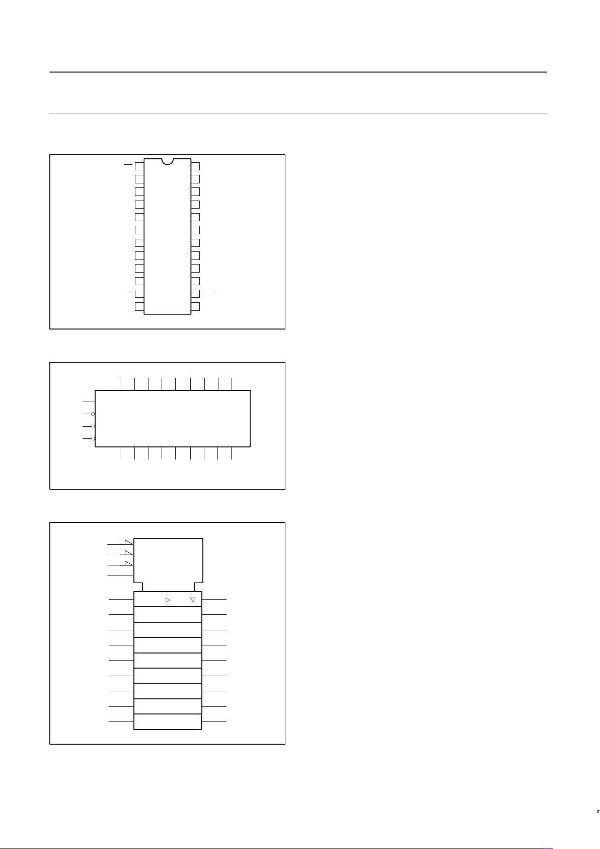
PIN CONFIGURATION for 74F842
1
2
3
4
5
6
7
8
9
10
11
12 13
14
15
16
17
18
19
20
21
22
23
24
OE
D0
D1
D2
D3
D4
D5
D6
D7
D8
D9
V
CC
Q0
Q
1
Q
2
Q
3
Q
4
Q
5
Q
7
Q6
Q
8
Q
9
LE
GND
SF01282
LOGIC SYMBOL for 74F842
13
2
SF01283
3456 78910
1
D0LED1 D2 D3 D4 D5 D6 D7 D8
OE
V
CC
= Pin 24
GND = Pin 12
11
D9
23 22 21 20 19 18 17 16 15 14
Q0 Q1 Q2 Q3 Q4 Q5 Q6 Q7 Q8 Q9
LOGIC SYMBOL (IEEE/IEC) for 74F842
1
15
18
19
20
21
232
1 D
SF01284
16
17
5
6
7
8
9
10
4
13
EN
C1
223
14
11
Page 4
Philips Semiconductors Product specification
74F841/74F842/74F843/
74F845/74F846
Bus interface latches
1999 Jun 23
4
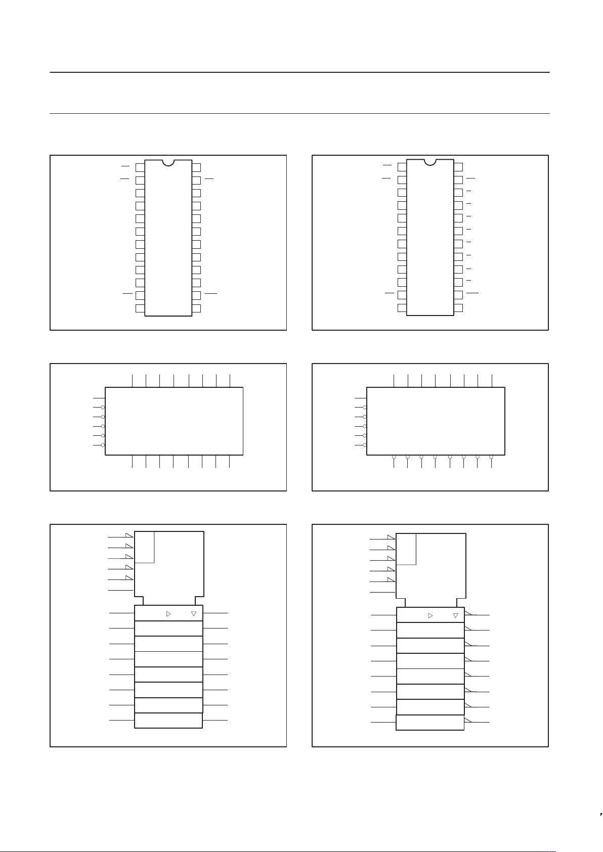
PIN CONFIGURATION for 74F843
1
2
3
4
5
6
7
8
9
10
11
12 13
14
15
16
17
18
19
20
21
22
23
24
OE
D0
D1
D2
D3
D4
D5
D6
D7
D8
MR
V
CC
Q0
Q1
Q2
Q3
Q4
Q5
Q7
Q6
Q8
PRE
LE
GND
SF01285
LOGIC SYMBOL for 74F843
13
2
SF01286
3456 78910
D0LED1 D2 D3 D4 D5 D6 D7 D8
V
CC
= Pin 24
GND = Pin 12
23 22 21 20 19 18 17 16 15
Q0 Q1 Q2 Q3 Q4 Q5 Q6 Q7 Q8
14 PRE
11 MR
1OE
LOGIC SYMBOL (IEEE/IEC) for 74F843
1
15
18
19
20
21
232
1 D
SF01287
16
17
5
6
7
8
9
10
4
11
14
13
EN
R
C1
S2
223
Page 5
Philips Semiconductors Product specification
74F841/74F842/74F843/
74F845/74F846
Bus interface latches
1999 Jun 23
5
PIN CONFIGURATION for 74F845
1
2
3
4
5
6
7
8
9
10
11
12 13
14
15
16
17
18
19
20
21
22
23
24
OE
0
OE
1
D0
D1
D2
D3
D4
D5
D6
D7
MR
V
CC
OE2
Q0
Q1
Q2
Q3
Q4
Q6
Q5
Q7
PRE
LE
GND
SF01291
LOGIC SYMBOL for 74F845
13
SF01292
3456 78910
D0LED1 D2 D3 D4 D5 D6 D7
V
CC
= Pin 24
GND = Pin 12
22 21 20 19 18 17 16 15
Q0 Q1 Q2 Q3 Q4 Q5 Q6 Q7
14 PRE
11 MR
1 OE0
2 OE1
23 OE2
LOGIC SYMBOL (IEEE/IEC) for 74F845
1
15
18
19
20
21
223
1 D
SF01293A
16
17
5
6
7
8
9
10
4
2
23
14
S2
11
R
13
C1
&
EN
PIN CONFIGURATION for 74F846
1
2
3
4
5
6
7
8
9
10
11
12 13
14
15
16
17
18
19
20
21
22
23
24
OE
0
OE
1
D0
D1
D2
D3
D4
D5
D6
D7
MR
V
CC
OE2
Q
0
Q
1
Q
2
Q
3
Q
4
Q
6
Q
5
Q
7
PRE
LE
GND
SF01294
LOGIC SYMBOL for 74F846
13
SF01295
3456 78910
D0LED1 D2 D3 D4 D5 D6 D7
V
CC
= Pin 24
GND = Pin 12
22 21 20 19 18 17 16 15
Q0 Q1 Q2 Q3 Q4 Q5 Q6 Q7
14 PRE
11 MR
1 OE0
2 OE1
23 OE2
LOGIC SYMBOL (IEEE/IEC) for 74F846
1
15
18
19
20
21
223
1 D
SF01296A
16
17
5
6
7
8
9
10
4
2
23
14
S2
11
R
13
C1
&
EN
Page 6
Philips Semiconductors Product specification
74F841/74F842/74F843/
74F845/74F846
Bus interface latches
1999 Jun 23
6
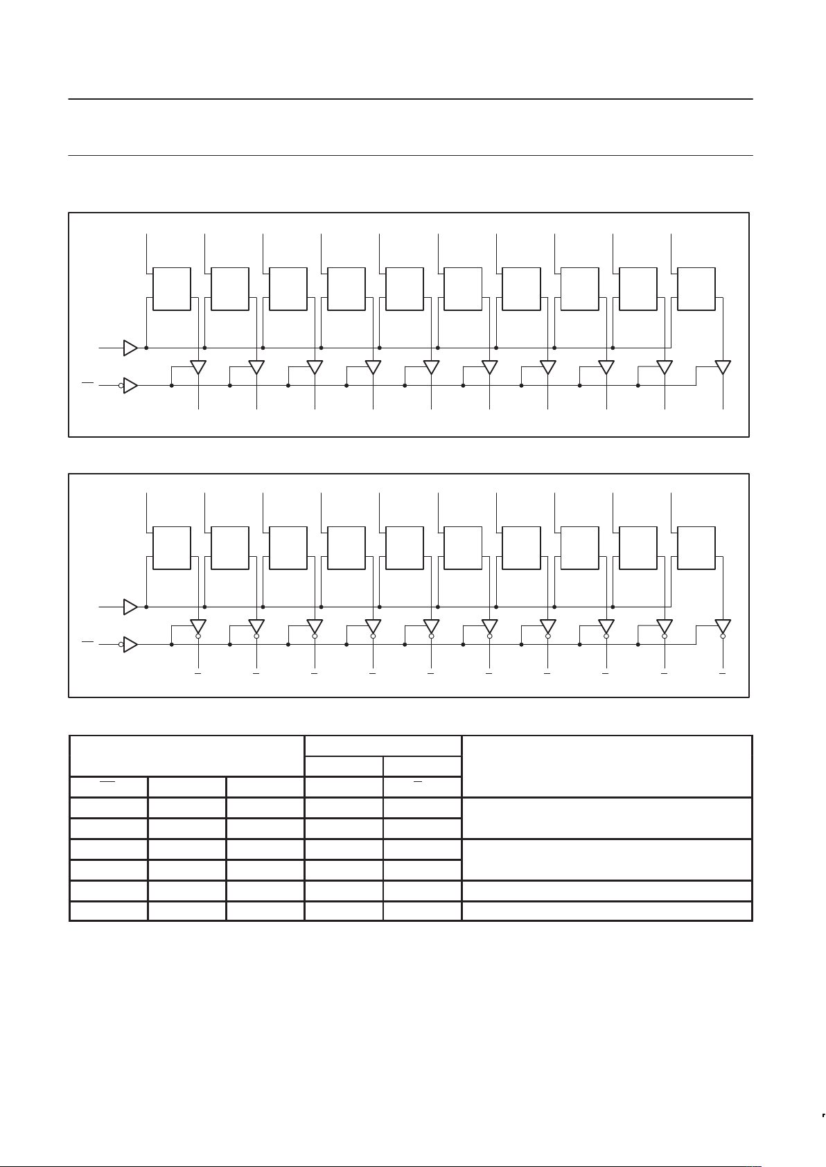
LOGIC DIAGRAM for 74F841
1
OE
VCC = Pin 24
GND = Pin 12
LQ
D
Q0
23
13
LE
D0
2
LQ
D
Q1
22
D1
3
LQ
D
Q2
21
D2
4
LQ
D
Q3
20
D3
5
LQ
D
Q4
19
D4
6
LQ
D
Q5
18
D5
7
LQ
C
D
Q6
17
D6
8
LQ
D
Q7
16
D7
9
LQ
D
Q8
15
D8
10
LQ
D
Q9
14
D9
11
SF01297
LOGIC DIAGRAM for 74F842
1
OE
VCC = Pin 24
GND = Pin 12
LQ
D
Q0
23
13
LE
D0
2
LQ
D
Q1
22
D1
3
LQ
D
Q2
21
D2
4
LQ
D
Q3
20
D3
5
LQ
D
Q4
19
D4
6
LQ
D
Q5
18
D5
7
LQ
C
D
Q6
17
D6
8
LQ
D
Q7
16
D7
9
LQ
D
Q8
15
D8
10
LQ
D
Q9
14
D9
11
SF01298
FUNCTION TABLE for 74F841 and 74F842
OUTPUTS
INPUTS
74F841 74F842
OPERATING MODE
OE LE Dn Qn Qn
L H L L H
p
L H H H L
Transparent
L ↓ l L H
L ↓ h H L
Latched
H X X Z Z High Impedance
L L X NC NC Hold
H = High voltage level
L = Low voltage level
h = High state one setup time before the High-to-Low LE transition
l = Low state one setup time before the High-to-Low LE transition
↓ = High-to-Low transition
X = Don’t care
NC= No change
Z = High impedance “off” state
Page 7

Philips Semiconductors Product specification
74F841/74F842/74F843/
74F845/74F846
Bus interface latches
1999 Jun 23
7
LOGIC DIAGRAM for 74F843
1
OE
VCC = Pin 24
GND = Pin 12
LQ
C
DP
Q0
23
13
LE
11
MR
14
PRE
D0
2
LQ
C
DP
Q1
22
D1
3
LQ
C
DP
Q2
21
D2
4
LQ
C
DP
Q3
20
D3
5
LQ
C
DP
Q4
19
D4
6
LQ
C
DP
Q5
18
D5
7
LQ
C
DP
Q6
17
D6
8
LQ
C
DP
Q7
16
D7
9
LQ
C
DP
Q8
15
D8
10
SF01299
FUNCTION TABLE for 74F843
OUTPUTS
INPUTS
74F843
OPERATING MODE
OE PRE MR LE Dn Qn
L L X X X H Preset
L H L X X L Clear
L H H H L L
p
L H H H H H
Transparent
L H H ↓ l L
L H H ↓ h H
Latched
H X X X X Z High Impedance
L H H L X NC Hold
H = High voltage level
L = Low voltage level
h = High state one setup time before the High-to-Low LE transition
l = Low state one setup time before the High-to-Low LE transition
↓ = High-to-Low transition
X = Don’t care
NC= No change
Z = High impedance “off” state
Page 8

Philips Semiconductors Product specification
74F841/74F842/74F843/
74F845/74F846
Bus interface latches
1999 Jun 23
8
LOGIC DIAGRAM for 74F845
1
2
23
OE
0
OE
1
OE2
V
CC
= Pin 24
GND = Pin 12
LQ
C
DP
Q0
22
13
LE
11
MR
14
PRE
D0
3
LQ
C
DP
Q1
21
D1
4
LQ
C
DP
Q2
20
D2
5
LQ
C
DP
Q3
19
D3
6
LQ
C
DP
Q4
18
D4
7
LQ
C
DP
Q5
17
D5
8
LQ
C
DP
Q6
16
D6
9
LQ
C
DP
Q7
15
D7
10
SF01301
LOGIC DIAGRAM for 74F846
1
2
23
OE
0
OE
1
OE2
V
CC
= Pin 24
GND = Pin 12
LQ
C
DP
Q0
22
13
LE
11
MR
14
PRE
D0
3
LQ
C
DP
Q1
21
D1
4
LQ
C
DP
Q2
20
D2
5
LQ
C
DP
Q3
19
D3
6
LQ
C
DP
Q4
18
D4
7
LQ
C
DP
Q5
17
D5
8
LQ
C
DP
Q6
16
D6
9
LQ
C
DP
Q7
15
D7
10
SF01302
FUNCTION TABLE for 74F845 and 74F846
OUTPUTS
INPUTS
74F845 74F846
OPERATING MODE
OE PRE MR LE Dn Qn Qn
L L X X X H H Preset
L H L X X L L Clear
L H H H L L H
p
L H H H H H L
Transparent
L H H ↓ l L H
L H H ↓ h H L
Latched
H X X X X Z Z High Impedance
L H H L X NC NC Hold
H = High voltage level
L = Low voltage level
h = High state one setup time before the High-to-Low LE transition
l = Low state one setup time before the High-to-Low LE transition
↓ = High-to-Low transition
X = Don’t care
NC= No change
Z = High impedance “off” state
Page 9

Philips Semiconductors Product specification
74F841/74F842/74F843/
74F845/74F846
Bus interface latches
1999 Jun 23
9
ABSOLUTE MAXIMUM RATINGS
Operation beyond the limits set forth in this table may impair the useful life of the device.
Unless otherwise noted these limits are over the operating free-air temperature range.
SYMBOL
PARAMETER RATING UNIT
V
CC
Supply voltage –0.5 to +7.0 V
V
IN
Input voltage –0.5 to +7.0 V
I
IN
Input current –30 to +5 mA
V
OUT
Voltage applied to output in High output state –0.5 to V
CC
V
I
OUT
Current applied to output in Low output state 84 mA
T
amb
Operating free-air temperature range 0 to +70 °C
T
stg
Storage temperature range –65 to +150 °C
RECOMMENDED OPERATING CONDITIONS
LIMITS
SYMBOL
PARAMETER
MIN NOM MAX
UNIT
V
CC
Supply voltage 4.5 5.0 5.5 V
V
IH
High-level input voltage 2.0 V
V
IL
Low-level input voltage 0.8 V
I
IK
Input clamp current –18 mA
I
OH
High-level output current –24 mA
I
OL
Low-level output current 48 mA
T
amb
Operating free-air temperature range 0 +70 °C
Page 10

Philips Semiconductors Product specification
74F841/74F842/74F843/
74F845/74F846
Bus interface latches
1999 Jun 23
10
DC ELECTRICAL CHARACTERISTICS
Over recommended operating free-air temperature range unless otherwise noted.
LIMITS
SYMBOL
PARAMETER
TEST CONDITIONS
1
MIN TYP2MAX
UNIT
±10%V
CC
2.2 V
p
VCC = MIN,
I
OH
= –
15mA
±5%V
CC
2.2 3.3 V
VOHHigh-level output voltage
CC
,
VIL = MAX, VIH = MIN
±10%V
CC
2.0 V
I
OH
= –
24mA
±5%V
CC
2.0 V
p
VCC = MIN,
IOL = 32mA ±10%V
CC
0.38 0.55 V
VOLLow-level output voltage
CC
,
VIL = MAX, VIH = MIN
IOL = 48mA ±5%V
CC
0.38 0.55 V
V
IK
Input clamp voltage VCC = MIN, II = I
IK
–0.73 –1.2 V
I
I
Input current at maximum input voltage VCC = 0.0V, VI = 7.0V 100 µA
I
IH
High-level input current VCC = MAX, VI = 2.7V 20 µA
I
IL
Low-level input current VCC = MAX, VI = 0.5V –20 µA
I
OZH
Off-state output current,
High-level voltage applied
VCC = MAX, VO = 2.7V 50 µA
I
OZL
Off-state output current,
Low-level voltage applied
VCC = MAX, VO = 0.5V –50 µA
I
OS
Short-circuit output current
3
VCC = MAX –100 –225 mA
I
CCH
50 65 mA
74F841
I
CCL
VCC = MAX
60 80 mA
I
CCZ
70 92 mA
I
CCH
40 60 mA
74F842
I
CCL
VCC = MAX
65 90 mA
Supply current
I
CCZ
60 90 mA
I
CC
y
(total)
I
CCH
65 90 mA
74F843
74F845
I
CCL
VCC = MAX
75 100 mA
74F845
I
CCZ
85 115 mA
I
CCH
50 70 mA
74F846
I
CCL
VCC = MAX
70 95 mA
I
CCZ
70 95 mA
NOTES:
1. For conditions shown as MIN or MAX, use the appropriate value specified under recommended operating conditions for the applicable type.
2. All typical values are at V
CC
= 5V, T
amb
= 25°C.
3. Not more than one output should be shorted at a time. For testing I
OS
, the use of high-speed test apparatus and/or sample-and-hold
techniques are preferable in order to minimize internal heating and more accurately reflect operational values. Otherwise, prolonged shorting
of a High output may raise the chip temperature well above normal and thereby cause invalid readings in other parameter tests. In any
sequence of parameter test, I
OS
tests should be performed last.
Page 11

Philips Semiconductors Product specification
74F841/74F842/74F843/
74F845/74F846
Bus interface latches
1999 Jun 23
11
AC ELECTRICAL CHARACTERISTICS for 74F841/74F842
LIMITS
T
amb
= +25°C T
amb
= 0°C to +70°C
SYMBOL PARAMETER TEST VCC = +5.0V VCC = +5.0V ± 10% UNIT
CONDITION CL = 50pF, RL = 500Ω CL = 50pF, RL = 500Ω
MIN TYP MAX MIN MAX
t
PLH
t
PHL
Propagation delay
Dn to Qn
Waveform 1, 2
2.0
2.5
4.0
4.5
7.5
7.5
2.0
2.5
8.0
8.0
ns
t
PLH
t
PHL
Propagation delay
LE to Qn
74F841
Waveform 1, 2
4.5
4.0
6.5
6.0
9.5
9.0
4.0
3.5
10.0
9.5
ns
t
PLH
t
PHL
Propagation delay
Dn to Qn
Waveform 1, 2
3.5
3.0
5.5
5.0
8.5
8.0
4.5
4.0
9.0
8.5
ns
t
PLH
t
PHL
Propagation delay
LE to Qn
74F842
Waveform 1, 2
5.0
4.5
7.0
6.5
10.0
9.0
3.0
3.0
10.5
9.5
ns
t
PZH
t
PZL
Output enable time
High or Low-level OEn to Qn or Qn
Waveform 5
Waveform 6
2.5
4.0
4.5
6.0
8.0
9.5
2.0
3.0
8.5
10.5
ns
t
PHZ
t
PLZ
Output disable time
High or Low-level OEn to Qn or Qn
Waveform 5
Waveform 6
1.0
1.0
4.5
5.0
8.0
8.0
1.0
1.0
8.5
8.5
ns
AC SETUP REQUIREMENTS for 74F841/74F842
LIMITS
T
amb
= +25°C T
amb
= 0°C to +70°C
SYMBOL PARAMETER TEST VCC = +5.0V VCC = +5.0V ± 10% UNIT
CONDITION CL = 50pF, RL = 500Ω CL = 50pF, RL = 500Ω
MIN TYP MIN MAX
ts(H)
ts(L)
Setup time, High or Low
Dn to LE
Waveform 4
0.0
0.0
1.0
1.0
ns
th(H)
th(L)
Hold time, High or Low
Dn to LE
74F841
Waveform 4
2.5
3.0
3.0
4.0
ns
tw(H) LE pulse width, High Waveform 4 3.5 4.0 ns
th(H)
th(L)
Hold time, High or Low
Dn to LE
74F842
Waveform 4
3.0
3.5
3.5
4.5
ns
tw(H) LE pulse width, High Waveform 4 3.0 3.0 ns
Page 12

Philips Semiconductors Product specification
74F841/74F842/74F843/
74F845/74F846
Bus interface latches
1999 Jun 23
12
AC ELECTRICAL CHARACTERISTICS for 74F843/74F845
LIMITS
T
amb
= +25°C T
amb
= 0°C to +70°C
SYMBOL PARAMETER TEST VCC = +5.0V VCC = +5.0V ± 10% UNIT
CONDITION CL = 50pF, RL = 500Ω CL = 50pF, RL = 500Ω
MIN TYP MAX MIN MAX
t
PLH
t
PHL
Propagation delay
Dn to Qn
Waveform 1, 2
2.0
2.5
4.5
4.5
7.5
8.0
2.0
2.5
8.5
8.5
ns
t
PLH
t
PHL
Propagation delay
LE to Qn
Waveform 1, 2
4.5
4.0
6.5
6.0
9.5
8.5
4.5
4.0
10.0
8.5
ns
t
PLH
Propagation delay
PRE to Qn
Waveform 3 3.5 5.5 8.5 3.0 9.0 ns
t
PHL
Propagation delay
MR to Qn
Waveform 3 2.0 4.5 7.5 2.0 8.0 ns
t
PZH
t
PZL
Output enable time
High or Low-level OEn to Qn
Waveform 5
Waveform 6
2.5
4.0
4.5
6.0
7.5
9.5
2.0
3.0
8.0
10.5
ns
t
PHZ
t
PLZ
Output disable time
High or Low-level OEn to Qn
Waveform 5
Waveform 6
1.0
1.0
4.5
5.0
8.0
8.0
1.0
1.0
8.5
8.5
ns
AC SETUP REQUIREMENTS for 74F843/74F845
LIMITS
T
amb
= +25°C T
amb
= 0°C to +70°C
SYMBOL PARAMETER TEST VCC = +5.0V VCC = +5.0V ± 10% UNIT
CONDITION CL = 50pF, RL = 500Ω CL = 50pF, RL = 500Ω
MIN TYP MIN MAX
ts(H)
ts(L)
Setup time, High or Low
Dn to LE
Waveform 4
1.0
1.0
0.0
0.0
ns
th(H)
th(L)
Hold time, High or Low
Dn to LE
Waveform 4
3.0
4.0
3.0
4.0
ns
tw(H) LE pulse width, High Waveform 4 3.0 3.0 ns
tw(L) PRE pulse width, Low Waveform 3 4.0 5.0 ns
tw(H) MR pulse width, Low Waveform 3 4.0 5.0 ns
t
REC
PRE recovery time Waveform 3 0.0 0.0 ns
t
REC
MR recovery time Waveform 3 3.5 4.5 ns
Page 13

Philips Semiconductors Product specification
74F841/74F842/74F843/
74F845/74F846
Bus interface latches
1999 Jun 23
13
AC ELECTRICAL CHARACTERISTICS for 74F846
LIMITS
T
amb
= +25°C T
amb
= 0°C to +70°C
SYMBOL PARAMETER TEST VCC = +5.0V VCC = +5.0V ± 10% UNIT
CONDITION CL = 50pF, RL = 500Ω CL = 50pF, RL = 500Ω
MIN TYP MAX MIN MAX
t
PLH
t
PHL
Propagation delay
Dn to Qn
Waveform 1, 2
3.5
3.0
5.5
5.0
8.5
8.0
3.0
3.0
9.5
8.5
ns
t
PLH
t
PHL
Propagation delay
LE to Qn
Waveform 1, 2
5.0
4.5
7.0
6.5
10.0
9.0
5.0
4.5
10.5
9.5
ns
t
PLH
Propagation delay
PRE to Qn
Waveform 3 3.5 5.5 8.5 3.0 9.5 ns
t
PHL
Propagation delay
MR to Qn
Waveform 3 5.0 7.0 10.0 4.5 10.5 ns
t
PZH
t
PZL
Output enable time
High or Low-level OEn to Qn
Waveform 5
Waveform 6
2.5
4.0
5.0
6.0
7.5
9.5
2.0
3.0
8.0
10.5
ns
t
PHZ
t
PLZ
Output disable time
High or Low-level OEn to Qn
Waveform 5
Waveform 6
1.0
1.0
4.5
5.0
8.0
8.0
1.0
1.0
8.5
8.5
ns
AC SETUP REQUIREMENTS for 74F846
LIMITS
T
amb
= +25°C T
amb
= 0°C to +70°C
SYMBOL PARAMETER TEST VCC = +5.0V VCC = +5.0V ± 10% UNIT
CONDITION CL = 50pF, RL = 500Ω CL = 50pF, RL = 500Ω
MIN TYP MIN MAX
ts(H)
ts(L)
Setup time, High or Low
Dn to LE
Waveform 4
0.0
0.0
0.0
0.0
ns
th(H)
th(L)
Hold time, High or Low
Dn to LE
Waveform 4
3.0
4.0
3.0
4.0
ns
tw(H) LE pulse width, High Waveform 4 3.0 3.0 ns
tw(L) PRE pulse width, Low Waveform 3 4.0 5.0 ns
tw(H) MR pulse width, Low Waveform 3 4.0 5.0 ns
t
REC
PRE recovery time Waveform 3 0.0 0.0 ns
t
REC
MR recovery time Waveform 3 3.5 4.5 ns
Page 14

Philips Semiconductors Product specification
74F841/74F842/74F843/
74F845/74F846
Bus interface latches
1999 Jun 23
14
AC WAVEFORMS
For all waveforms, VM = 1.5V .
The shaded areas indicate when the input is permitted to change for predictable output performance.
V
M
V
M
V
M
V
M
t
PHL
t
PLH
Dn, LE
Qn
SF01303
Waveform 1. Propagation Delay, Non-Inverting Path
V
M
V
M
V
M
V
M
t
PLH
t
PHL
Dn, LE
Q
n
SF01304
Waveform 2. Propagation Delay, Inverting Path
LE
V
M
V
M
PRE,
MR
V
M
tw(L)
t
REC
V
M
V
M
t
PLH
t
PHL
Qn, Qn
Qn, Q
n
SF01305
Waveform 3. Master Reset and Preset Pulse Width,
Master Reset and Preset to Output Delay,
and Master Reset and Preset to Latch Enable Recovery Time
th(H)ts(H)
LE
V
M
V
M
V
M
V
M
V
M
V
M
th(L)ts(L)
Dn
V
M
tw(H)
SF01306
Waveform 4. Data Setup and Hold Times
V
M
V
M
V
M
t
PHZ
t
PZH
OEn
VOH -0.3V
0V
Qn, Qn
SF00509
Waveform 5. 3-State Output Enable Time to High Level
and Output Disable Time from High Level
V
M
V
M
V
M
t
PLZ
t
PZL
VOL +0.3V
3.5V
OEn
Qn, Q
n
SF00510
Waveform 6. 3-State Output Enable Time to Low Level
and Output Disable time from Low Level
Page 15

Philips Semiconductors Product specification
74F841/74F842/74F843/
74F845/74F846
Bus interface latches
1999 Jun 23
15
TEST CIRCUIT AND WAVEFORMS
t
w
90%
V
M
10%
90%
V
M
10%
90%
V
M
10%
90%
V
M
10%
NEGATIVE
PULSE
POSITIVE
PULSE
t
w
AMP (V)
0V
0V
t
THL (tf
)
INPUT PULSE REQUIREMENTS
rep. rate
t
w
t
TLHtTHL
1MHz 500ns
2.5ns 2.5ns
Input Pulse Definition
V
CC
family
74F
D.U.T.
PULSE
GENERATOR
R
L
C
L
R
T
V
IN
V
OUT
Test Circuit for 3-State Outputs
DEFINITIONS:
R
L
= Load resistor;
see AC electrical characteristics for value.
C
L
= Load capacitance includes jig and probe capacitance;
see AC electrical characteristics for value.
R
T
= Termination resistance should be equal to Z
OUT
of
pulse generators.
t
THL (tf
)
t
TLH (tr
)
t
TLH (tr
)
AMP (V)
amplitude
3.0V
1.5V
V
M
R
L
7.0V
SF00777
TEST SWITCH
t
PLZ
closed
t
PZL
closed
All other open
SWITCH POSITION
Page 16

Philips Semiconductors Product specification
74F841/74F842/74F843/
74F845/74F846
Bus interface latches
1999 Jun 23
16
DIP24: plastic dual in-line package; 24 leads (300 mil) SOT222-1
Page 17

Philips Semiconductors Product specification
74F841/74F842/74F843/
74F845/74F846
Bus interface latches
1999 Jun 23
17
SO24: plastic small outline package; 24 leads; body width 7.5 mm SOT137-1
Page 18

Philips Semiconductors Product specification
74F841/74F842/74F843/
74F845/74F846
Bus interface latches
1999 Jun 23
18
Definitions
Short-form specification — The data in a short-form specification is extracted from a full data sheet with the same type number and title. For
detailed information see the relevant data sheet or data handbook.
Limiting values definition — Limiting values given are in accordance with the Absolute Maximum Rating System (IEC 134). Stress above one
or more of the limiting values may cause permanent damage to the device. These are stress ratings only and operation of the device at these or
at any other conditions above those given in the Characteristics sections of the specification is not implied. Exposure to limiting values for extended
periods may affect device reliability.
Application information — Applications that are described herein for any of these products are for illustrative purposes only. Philips
Semiconductors make no representation or warranty that such applications will be suitable for the specified use without further testing or
modification.
Disclaimers
Life support — These products are not designed for use in life support appliances, devices or systems where malfunction of these products can
reasonably be expected to result in personal injury . Philips Semiconductors customers using or selling these products for use in such applications
do so at their own risk and agree to fully indemnify Philips Semiconductors for any damages resulting from such application.
Right to make changes — Philips Semiconductors reserves the right to make changes, without notice, in the products, including circuits, standard
cells, and/or software, described or contained herein in order to improve design and/or performance. Philips Semiconductors assumes no
responsibility or liability for the use of any of these products, conveys no license or title under any patent, copyright, or mask work right to these
products, and makes no representations or warranties that these products are free from patent, copyright, or mask work right infringement, unless
otherwise specified.
Philips Semiconductors
811 East Arques Avenue
P.O. Box 3409
Sunnyvale, California 94088–3409
Telephone 800-234-7381
Copyright Philips Electronics North America Corporation 1999
All rights reserved. Printed in U.S.A.
Date of release: 06-99
Document order number: 9397 750 06143
Data sheet
status
Objective
specification
Preliminary
specification
Product
specification
Product
status
Development
Qualification
Production
Definition
[1]
This data sheet contains the design target or goal specifications for product development.
Specification may change in any manner without notice.
This data sheet contains preliminary data, and supplementary data will be published at a later date.
Philips Semiconductors reserves the right to make changes at any time without notice in order to
improve design and supply the best possible product.
This data sheet contains final specifications. Philips Semiconductors reserves the right to make
changes at any time without notice in order to improve design and supply the best possible product.
Data sheet status
[1] Please consult the most recently issued datasheet before initiating or completing a design.
 Loading...