

Page 1

74F821/822/823/824/825/826
Bus interface registers
Product specification 1996 Jan 05
INTEGRATED CIRCUITS
IC15 Data Handbook
Page 2
Philips Semiconductors Product specification
74F821/822/823/824/825/826Bus interface registers
2
1996 Jan 05 853-1304 16195
74F821 10-bit bus interface register, non-inverting (3-State)
74F822 10-bit bus interface register, inverting (3-State)
74F823 9-bit bus interface register, non-inverting (3-State)
74F824 9-bit bus interface register, inverting (3-State)
74F825 8-bit bus interface register, non-inverting (3-State)
74F826 8-bit bus interface register, inverting (3-State)
FEATURES
•High speed parallel registers with positive edge-triggered D-type
flip-flops
•High performance bus interface buffering for wide data/address
paths or busses carrying parity
•High impedance PNP base inputs for reduced loading (20µA in
high and low states)
•I
IL
is 20µA vs 1000µA for AM29821 series
•Buffered control inputs to reduce AC effects
•Ideal where high speed, light loading, or increased fan-in as
required with MOS microprocessor
•Positive and negative over-shoots are clamped to ground
•3-State outputs glitch free during power-up and power-down
•Slim Dip 300 mil package
•Broadside pinout compatible with AMD AM 29821-29826 series
•Outputs sink 64mA and source 24mA
•Industrial temperature range available (–40°C to +85°C) for
74F823
DESCRIPTION
The 74F821 series bus interface registers are designed to
eliminate the extra packages required to buffer existing registers and
provide extra data width for wider data/address paths of busses
carrying parity.
The 74F821/74F822 are buffered 10-bit wide versions of the popular
74F374/74F534 functions.
The 74F822 is the inverted output version of 74F821.
The 74F823 and 74F824 are 9-bit wide buffered registers with clock
enable (CE
) and master reset (MR) which are ideal for parity bus
interfacing in high microprogrammed systems.
The 74F824 is the inverted version of 74F823.
The 74F825 and 74F826 are 8-bit buffered registers with all the
74F823/74F824 controls plus output enable (OE
0, OE1, OE2) to
allow multiuser control of the interface, e.g., CS
, DMA, and RD/WR.
They are ideal for uses as an output port requiring high I
OL/IOH
.
The 74F826 is the inverted version of 74F825.
TYPE
TYPICAL
f
max
TYPICAL
SUPPLY CURRENT
(TOTAL)
74F821, 74F822 180MHz 75mA
74F823, 74F824 180MHz 70mA
74F825, 74F826 180MHz 65mA
ORDERING INFORMATION
ORDER CODE
DESCRIPTION
COMMERCIAL RANGE
V
CC
= 5V ±10%,
T
amb
= 0°C to +70°C
INDUSTRIAL RANGE
V
CC
= 5V ±10%,
T
amb
= –40°C to +85°C
PKG. DWG. #
24-pin plastic slim DIP (300mil)
N74F821N, N74F822N, N74F823N,
N74F824N, N74F825N, N74F826N
I74F823N SOT222-1
24-pin plastic SOL
N74F821D, N74F822D, N74F823D,
N74F824D, N74F825D, N74F826D
I74F823D SOT137-1
Page 3
Philips Semiconductors Product specification
74F821/822/823/824/825/826Bus interface registers
1996 Jan 05
3
INPUT AND OUTPUT LOADING AND FAN OUT TABLE
PINS DESCRIPTION
74F (U.L.)
HIGH/LOW
LOAD VALUE
HIGH/LOW
Dn Data inputs 1.0/1.0 20µA/0.6mA
74F821 CP Clock input 1.0/1.0 20µA/0.6mA
74F822 OE Output enable input (active low) 1.0/3.0 20µA/1.8mA
Qn, Qn Data outputs 1200/106.7 24mA/64mA
Dn Data inputs 1.0/1.0 20µA/0.6mA
CP Clock input 1.0/1.0 20µA/0.6mA
74F823 CE Clock enable input (active low) 1.0/3.0 20µA/1.8mA
74F824 MR Master reset input (active low) 1.0/3.0 20µA/1.8mA
OE Output enable input (active low) 1.0/3.0 20µA/1.8mA
Qn, Qn Data outputs 1200/106.7 24mA/64mA
Dn Data inputs 1.0/1.0 20µA/0.6mA
CP Clock input 1.0/1.0 20µA/0.6mA
74F825 CE Clock enable input (active low) 1.0/3.0 20µA/1.8mA
74F826 MR Master reset input (active low) 1.0/3.0 20µA/1.8mA
OE Output enable input (active low) 1.0/3.0 20µA/1.8mA
Qn, Qn Data outputs 1200/106.7 24mA/64mA
NOTE: One (1.0) FAST unit load is defined as: 20µA in the high state and 0.6mA in the low state.
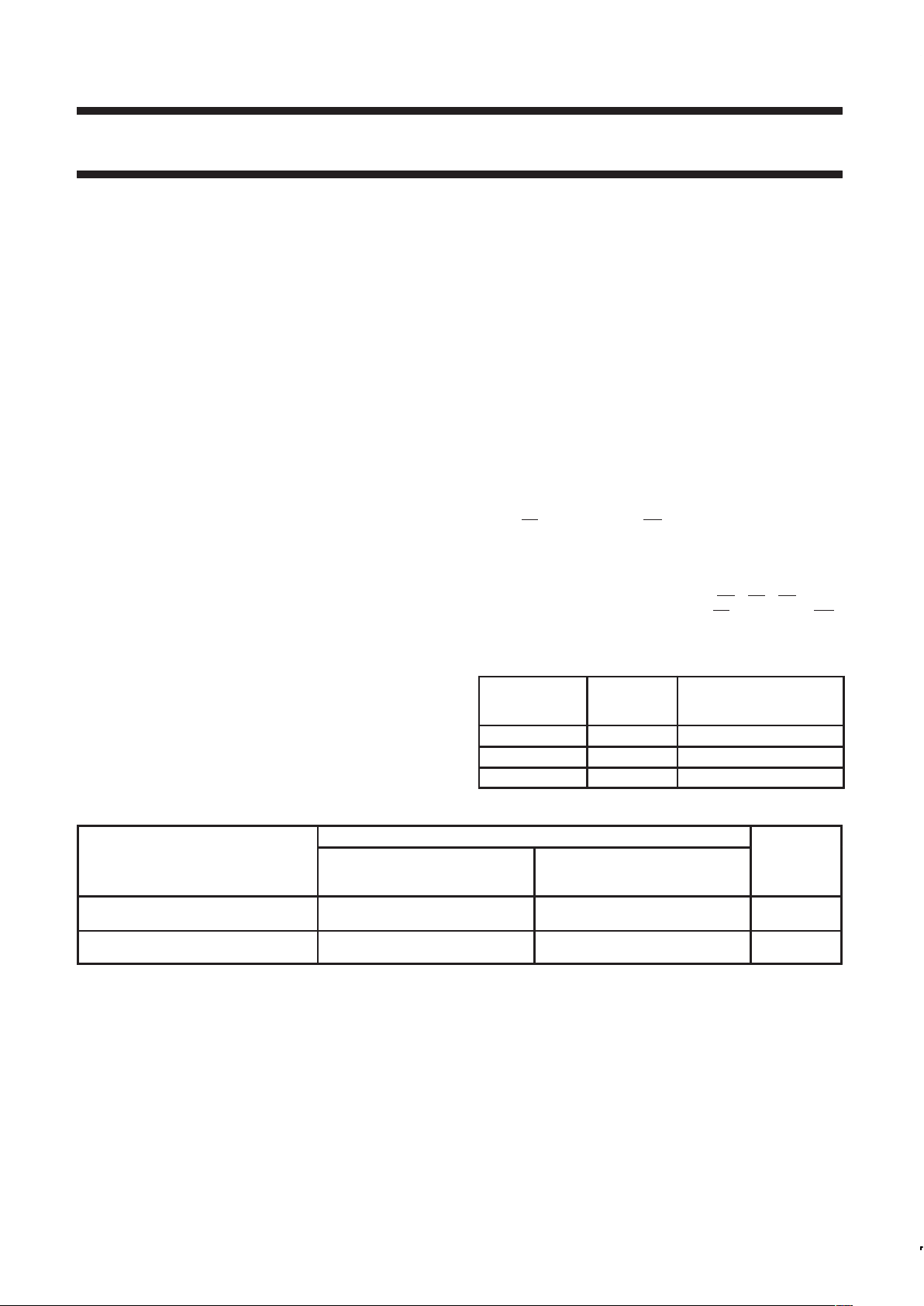
PIN CONFIGURATION – 74F821
24
23
22
21
20
19
18
17
16
15
14
1312
10
11
9
8
7
6
5
4
3
2
1
GND
OE
CP
Q0
Q3
Q4
Q5
Q6
V
CC
Q7
Q1
Q2
Q8
Q9
D0
D3
D4
D5
D6
D7
D1
D2
D8
D9
SF00482
LOGIC SYMBOL – 74F821
CP
OE
Q0 Q1 Q2 Q3 Q4 Q5 Q6 Q7
13
1
D0 D1 D2 D3 D4 D5 D6 D7
23456789
23 22 21 20 19 18 17 16
V
CC
= Pin 24
GND = Pin 12
D8 D9
10 11
Q8 Q9
15 14
SF00483
Page 4

Philips Semiconductors Product specification
74F821/822/823/824/825/826Bus interface registers
1996 Jan 05
4
IEC/IEEE SYMBOL – 74F821
1
G2
2
3
4
5
6
7
8
9
10
11
EN1
1
13
2D
23
22
21
20
19
18
17
16
15
14
SF00484
PIN CONFIGURATION – 74F822
24
23
22
21
20
19
18
17
16
15
14
1312
10
11
9
8
7
6
5
4
3
2
1
GND
OE
CP
Q
0
Q
3
Q4
Q
5
Q
6
V
CC
Q7
Q
1
Q
2
Q
8
Q
9
D0
D3
D4
D5
D6
D7
D1
D2
D8
D9
SF00485
LOGIC SYMBOL – 74F822
CP
OE
Q0 Q1 Q2 Q3 Q4 Q5 Q6 Q7
13
1
D0 D1 D2 D3 D4 D5 D6 D7
23456789
23 22 21 20 19 18 17 16
V
CC
= Pin 24
GND = Pin 12
D8 D9
10 11
Q8 Q9
15 14
SF00486
IEC/IEEE SYMBOL – 74F822
1
G2
2
3
4
5
6
7
8
9
10
11
EN1
1
13
2D
23
22
21
20
19
18
17
16
15
14
SF00487
PIN CONFIGURATION – 74F823
24
23
22
21
20
19
18
17
16
15
14
1312
10
11
9
8
7
6
5
4
3
2
1
GND
OE
CP
Q0
Q3
Q4
Q5
Q6
V
CC
Q7
Q1
Q2
Q8
CE
D0
D3
D4
D5
D6
D7
D1
D2
D8
MR
SF00488
LOGIC SYMBOL – 74F823
CP
CE
MR
OE
Q0 Q1 Q2 Q3 Q4 Q5 Q6 Q7
13
14
11
1
D0 D1 D2 D3 D4 D5 D6 D7
23456789
23 22 21 20 19 18 17 16
V
CC
= Pin 24
GND = Pin 12
D8
10
Q8
15
SF00489
Page 5

Philips Semiconductors Product specification
74F821/822/823/824/825/826Bus interface registers
1996 Jan 05
5
IEC/IEEE SYMBOL – 74F823
1
1G2
2
3
4
5
6
7
8
9
10
1
11
14
13
2D
23
22
21
20
19
18
17
16
15
EN1
R
G1
SF00490
PIN CONFIGURATION – 74F824
24
23
22
21
20
19
18
17
16
15
14
1312
10
11
9
8
7
6
5
4
3
2
1
GND
OE
CP
Q
0
Q
3
Q4
Q
5
Q
6
V
CC
Q7
Q
1
Q
2
Q
8
CE
D0
D3
D4
D5
D6
D7
D1
D2
D8
MR
SF00491
LOGIC SYMBOL – 74F824
CP
CE
MR
OE
Q0 Q1 Q2 Q3 Q4 Q5 Q6 Q7
13
14
11
1
D0 D1 D2 D3 D4 D5 D6 D7
23456789
23 22 21 20 19 18 17 16
V
CC
= Pin 24
GND = Pin 12
D8
10
Q8
15
SF00492
IEC/IEEE SYMBOL – 74F824
1
1G2
2
3
4
5
6
7
8
9
10
1
11
14
13
2D
23
22
21
20
19
18
17
16
15
EN1
R
G1
SF00493
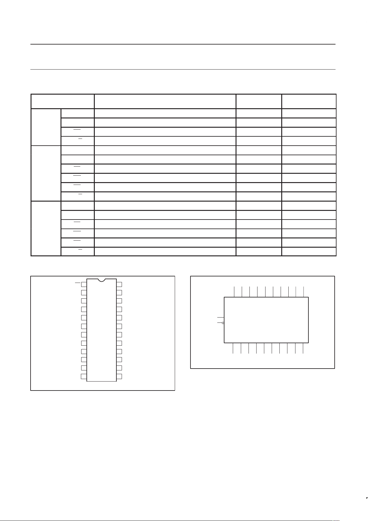
PIN CONFIGURATION – 74F825
24
23
22
21
20
19
18
17
16
15
14
1312
10
11
9
8
7
6
5
4
3
2
1
V
CC
OE2
QO
Q1
Q2
Q3
Q4
Q5
Q6
Q7
CE
CP
OE
0
OE
I
DO
D1
D2
D3
D4
D5
D6
D7
MR
GND
SF00494
LOGIC SYMBOL – 74F825
CP
CE
MR
OE0
OE1
OE2
Q0 Q1 Q2 Q3 Q4 Q5 Q6 Q7
13
14
11
1
2
23
D0 D1 D2 D3 D4 D5 D6 D7
3456789
22 21 20 19 18 17 16
V
CC
= Pin 24
GND = Pin 12
10
15
SF00495
Page 6
Philips Semiconductors Product specification
74F821/822/823/824/825/826Bus interface registers
1996 Jan 05
6
IEC/IEEE SYMBOL – 74F825
1
1G2
3
4
5
6
7
8
9
10
1
2
23
11
14
13
2D
22
21
20
19
18
17
16
15
R
G1
EN
&
SF00496
PIN CONFIGURATION – 74F826
24
23
22
21
20
19
18
17
16
15
14
1312
10
11
9
8
7
6
5
4
3
2
1
V
CC
OE0
OE
I
DO
D1
D2
D3
D4
D5
D6
D7
MR
GND
OE
2
QO
Q1
Q2
Q3
Q4
Q5
Q6
Q7
CE
CP
SF00497
LOGIC SYMBOL – 74F826
CP
CE
MR
OE0
OE1
OE2
Q0 Q1 Q2 Q3 Q4 Q5 Q6 Q7
13
14
11
1
2
23
D0 D1 D2 D3 D4 D5 D6 D7
3456789
22 21 20 19 18 17 16
V
CC
= Pin 24
GND = Pin 12
10
15
SF00498
IEC/IEEE SYMBOL – 74F826
1
1G2
3
4
5
6
7
8
9
10
1
2
23
11
14
13
2D
22
21
20
19
18
17
16
15
R
G1
EN
&
SF00499
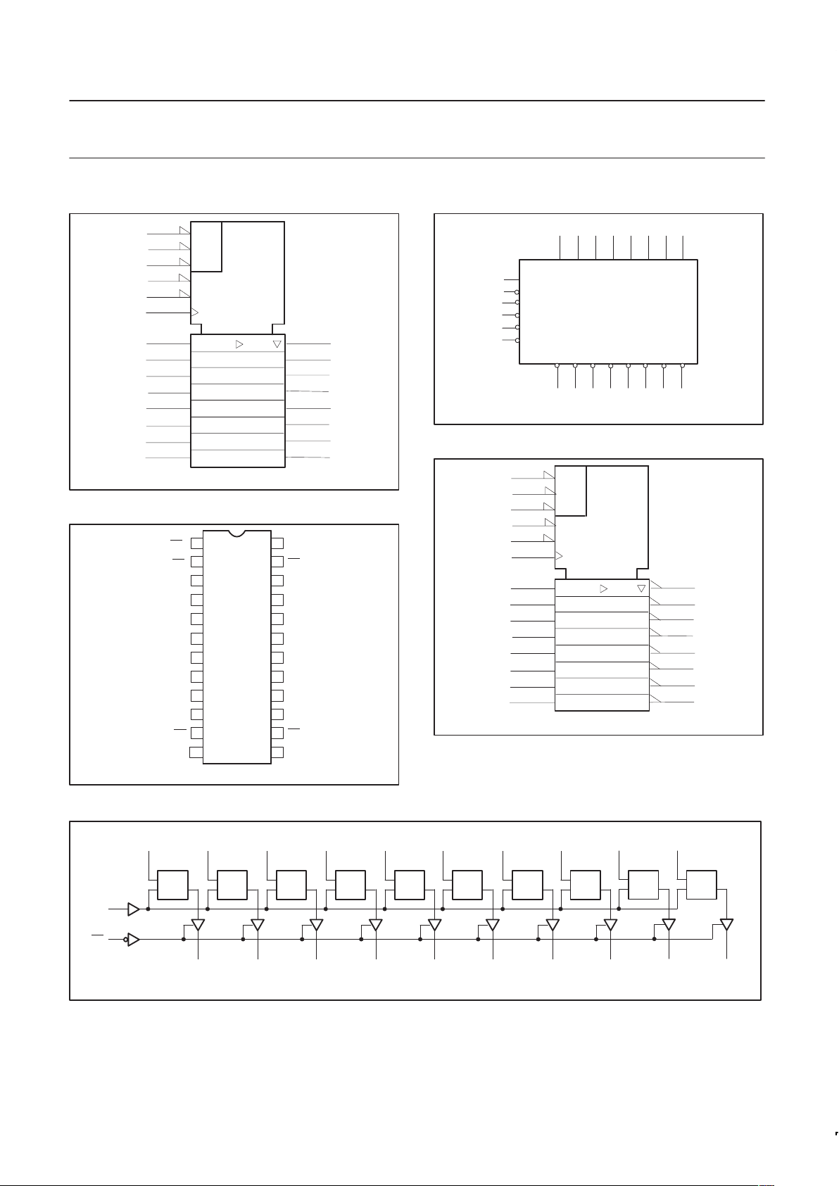
LOGIC DIAGRAM FOR 74F821
VCC = Pin 24
GND = Pin 12
D0
D
CP
Q
Q0
2
23
D1
D
CP
Q
Q1
3
22
D2
D
CP
Q
Q2
4
21
D3
D
CP
Q
Q3
5
20
D4
D
CP
Q
Q4
6
19
D5
D
CP
Q
Q5
7
18
D6
D
CP
Q
Q6
8
17
D7
D
CP
Q
Q7
9
16
D8
D
CP
Q
Q8
10
15
D9
D
CP
Q
Q9
11
14
13
1
CP
OE
SF00500
Page 7

Philips Semiconductors Product specification
74F821/822/823/824/825/826Bus interface registers
1996 Jan 05
7
LOGIC DIAGRAM FOR 74F822
VCC = Pin 24
GND = Pin 12
D
CP
Q
Q0
23
D
CP
Q
Q
1
22
D
CP
Q
Q
2
21
D
CP
Q
Q
3
20
D
CP
Q
Q
4
19
D
CP
Q
Q
5
18
D
CP
Q
Q
6
17
D
CP
Q
Q
7
16
D
CP
Q
Q
8
15
D
CP
Q
Q9
14
13
CP
D0
2
D1
3
D2
4
D3
5
D4
6
D5
7
D6
8
D7
9
D8
10
D9
11
SF00501
1
OE
FUNCTION TABLE FOR 74F821 AND 74F822
OUTPUTS
INPUTS
74F821 74F822
OPERATING MODE
OE CP Dn Q Q
L ↑ l L H
L ↑ h H L
Load and read data
L ↑ X NC NC Hold
H X X Z Z High impedance
H = High-voltage level
h = High state must be present one setup time before the low-to-high clock transition
L = Low-voltage level
l = Low state must be present one setup time before the low-to-high clock transition
NC= No change
X = Don’t care
Z = High impedance “off” state
↑ = Low-to-high clock transition
↑
= Not low-to-high clock transition
LOGIC DIAGRAM FOR 74F823
V
CC
= Pin 24
GND = Pin 12
D0
D
R
Q
Q0
2
23
D1
Q1
3
22
D2
Q2
4
21
D3
Q3
5
20
D4
Q4
6
19
D5
Q5
7
18
D6
Q6
8
17
D7
Q7
9
16
D8
Q8
10
15
11
MR
CP
CE
14
SF00502A
CP
13
OE
1
D
R
Q
CP
D
R
Q
CP
D
R
Q
CP
D
R
Q
CP
D
R
Q
CP
D
R
Q
CP
D
R
Q
CP
D
R
Q
CP
Page 8

Philips Semiconductors Product specification
74F821/822/823/824/825/826Bus interface registers
1996 Jan 05
8
LOGIC DIAGRAM FOR 74F824
VCC = Pin 24
GND = Pin 12
D0
D
R
Q
Q0
2
23
D1
Q
1
3
22
D2
Q
2
4
21
D3
Q
3
5
20
D4
Q
4
6
19
D5
Q
5
7
18
D6
Q
6
8
17
D7
Q
7
9
16
D8
Q
8
10
15
11
MR
CP
CE
14
SF00503A
1
OE
13
CP
D
R
Q
CP
D
R
Q
CP
D
R
Q
CP
D
R
Q
CP
D
R
Q
CP
D
R
Q
CP
D
R
Q
CP
D
R
Q
CP
FUNCTION TABLE for 74F823 and 74F824
OUTPUTS
INPUTS
74F823 74F824
OPERATING MODE
OE MR CE* CP Dn Q Q
L L X X X L L Clear
L H L ↑ h H L
L H L ↑ l L H
Load and read data
L H H X X NC NC Hold
H X X X X Z Z High impedance
H = High-voltage level
h = High state must be present one setup time before the low-to-high clock transition
L = Low-voltage level
l = Low state must be present one setup time before the low-to-high clock transition
NC= No change
X = Don’t care
Z = High impedance “off” state
* = Since CE
input is sensitive to very short (<3ns) high-to-low-to-high going spikes while CP is high, users should avoid the use of decoders
or other potentially glitch prone device on the CE
input.
↑ = Low-to-high clock transition
LOGIC DIAGRAM FOR 74F825
VCC = Pin 24
GND = Pin 12
D0
D
R
Q
Q0
3
22
D1
Q1
4
21
D2
Q2
5
20
D3
Q3
6
19
D4
Q4
7
18
D5
Q5
8
17
D6
Q6
9
16
D7
Q7
10
15
11
MR
CP
CE
14
1
OE
0
SF00504A
13
CP
23
2
OE1
OE
2
D
R
Q
CP
D
R
Q
CP
D
R
Q
CP
D
R
Q
CP
D
R
Q
CP
D
R
Q
CP
D
R
Q
CP
Page 9

Philips Semiconductors Product specification
74F821/822/823/824/825/826Bus interface registers
1996 Jan 05
9
LOGIC DIAGRAM FOR 74F826
V
CC
= Pin 24
GND = Pin 12
D0
D
R
Q
Q0
D1
Q
1
3
22
D2
Q
2
4
21
D3
Q
3
5
20
D4
Q
4
6
19
D5
Q
5
7
18
D6
Q
6
8
17
D7
Q
7
9
16
10
15
CP
CE
14
11
MR
1
OE
0
SF00505A
13
CP
2
23
OE
1
OE
2
D
R
Q
CP
D
R
Q
CP
D
R
Q
CP
D
R
Q
CP
D
R
Q
CP
D
R
Q
CP
D
R
Q
CP
FUNCTION TABLE FOR 74F825 AND 74F826
OUTPUTS
INPUTS
74F825 74F826
OPERATING MODE
OEn MR CE* CP Dn Q Q
L L X X X L L Clear
L H L ↑ h H L
L H L ↑ l L H
Load and read data
L H H X X NC NC Hold
H X X X X Z Z High impedance
H = High-voltage level
h = High state must be present one setup time before the low-to-high clock transition
L = Low-voltage level
l = Low state must be present one setup time before the low-to-high clock transition
NC= No change
X = Don’t care
Z = High impedance “off” state
* = Since CE
input is sensitive to very short (<3ns) high-to-low-to-high going spikes while CP is high, users should avoid the use of decoders
or other potentially glitch prone device on the CE
input.
↑ = Low-to-high clock transition
ABSOLUTE MAXIMUM RATINGS
(Operation beyond the limit set forth in this table may impair the useful life of the device.
Unless otherwise noted these limits are over the operating free-air temperature range.)
SYMBOL
PARAMETER RATING UNIT
V
CC
Supply voltage –0.5 to +7.0 V
V
IN
Input voltage –0.5 to +7.0 V
I
IN
Input current –30 to +5 mA
V
OUT
Voltage applied to output in high output state –0.5 to V
CC
V
I
OUT
Current applied to output in low output state 128 mA
p
p
Commercial range 0 to +70 °C
T
amb
Operating free-air temperature range
Industrial range –40 to +85 °C
T
stg
Storage temperature range –65 to +150 °C
Page 10

Philips Semiconductors Product specification
74F821/822/823/824/825/826Bus interface registers
1996 Jan 05
10
RECOMMENDED OPERATING CONDITIONS
PARAMETER
LIMITS
SYMBOL
MIN NOM MAX
UNIT
V
CC
Supply voltage 4.5 5.0 5.5 V
V
IH
High-level input voltage 2.0 V
V
IL
Low-level input voltage 0.8 V
I
Ik
Input clamp current –18 mA
I
OH
High–level output current –24 mA
I
OL
Low–level output current 64 mA
p
p
Commercial range 0 +70 °C
T
amb
O erating free-air tem erature range
Industrial range –40 +85 °C
DC ELECTRICAL CHARACTERISTICS
(Over recommended operating free-air temperature range unless otherwise noted.)
LIMITS
SYMBOL
PARAMETER
TEST CONDITIONS
1
MIN TYP2MAX
UNIT
±10%V
CC
2.4 V
p
VCC = MIN,
I
OH
= –
15mA
±5%V
CC
2.4 V
VOHHigh-level output voltage
V
IL
=
MAX
,
VIH = MIN
±10%V
CC
2.0 V
I
OH
= –
24mA
±5%V
CC
2.0 V
p
VCC = MIN,
±10%V
CC
0.55 V
VOLLow-level output voltage
V
IL
=
MAX
,
V
IH
= MIN
I
OL
=
MAX
±5%V
CC
0.42 0.55 V
V
IK
Input clamp voltage VCC = MIN, II = I
IK
–0.73 –1.2 V
I
I
Input current at maximum input voltage VCC = 0.0V, VI = 7.0V 100 µA
I
IH
High–level input current VCC = MAX, VI = 2.7V 20 µA
I
IL
Low–level input current VCC = MAX, VI = 0.5V –20 µA
I
OZH
Off–state output current, high–level voltage applied VCC = MAX, V
O
= 2.7V 50 µA
I
OZL
Off–state output current, low–level voltage applied VCC = MAX, VO = 0.5V –50 µA
I
OS
Short–circuit output current
3
VCC = MAX -100 -225 mA
I
CCH
75 105 mA
74F821,
I
CCL
VCC = MAX
75 105 mA
74F822
I
CCZ
75 115 mA
I
CCH
65 100 mA
I
CC
Supply current (total)
74F823,
I
CCL
VCC = MAX
70 105 mA
74F824
I
CCZ
75 110 mA
I
CCH
60 85 mA
74F825,
I
CCL
VCC = MAX
60 90 mA
74F826
I
CCZ
65 95 mA
NOTES:
1. For conditions shown as MIN or MAX, use the appropriate value specified under recommended operating conditions for the applicable type.
2. All typical values are at V
CC
= 5V, T
amb
= 25°C.
3. Not more than one output should be shorted at a time. For testing I
OS
, the use of high-speed test apparatus and/or sample-and-hold
techniques are preferable in order to minimize internal heating and more accurately reflect operational values. Otherwise, prolonged shorting
of a high output may raise the chip temperature well above normal and thereby cause invalid readings in other parameter tests. In any
sequence of parameter tests, I
OS
tests should be performed last.
Page 11

Philips Semiconductors Product specification
74F821/822/823/824/825/826Bus interface registers
1996 Jan 05
11
AC ELECTRICAL CHARACTERISTICS FOR 74F821/74F822/74F824/74F825/74F826
LIMITS
SYMBOL PARAMETER
TEST
CONDITION
T
amb
= +25°C
VCC = +5.0V
C
L
= 50pF, RL = 500Ω
T
amb
= 0°C to +70°C
VCC = +5.0V ± 10%
C
L
= 50pF, RL = 500Ω
UNIT
MIN TYP MAX MIN MAX
f
max
Maximum clock frequency Waveform 1 150 180 140 ns
t
PLH
t
PHL
Propagation delay
CP to Qn or Qn
74F821,
74F825, 74F826
Waveform 1
4.0
4.0
6.5
6.0
8.5
8.5
4.0
3.5
9.5
9.0
ns
t
PLH
t
PHL
Propagation delay
CP to Qn
74F822, 74F824 Waveform 1
4.5
4.5
6.5
6.5
9.0
9.0
4.5
4.5
10.0
9.0
ns
t
PHL
Propagation delay
MR to Qn or Qn
74F824
74F825, 74F826
Waveform 2 3.0 5.0 8.0 3.0 8.0 ns
t
PZH
t
PZL
Output enable time
OEn to Qn or Qn
Waveform 4
Waveform 5
2.0
3.0
4.5
5.0
8.0
8.0
2.0
2.5
9.0
9.0
ns
t
PHZ
t
PLZ
Output disable time
OEn to Qn or Qn
Waveform 4
Waveform 5
1.5
1.5
3.5
3.5
6.5
6.5
1.5
1.5
7.5
7.5
ns
AC SETUP REQUIREMENTS FOR 74F821/74F822/74F824/74F825/74F826
LIMITS
SYMBOL PARAMETER
TEST
CONDITION
T
amb
= +25°C
VCC = +5.0V
C
L
= 50pF, RL = 500Ω
T
amb
= 0°C to +70°C
VCC = +5.0V ± 10%
C
L
= 50pF, RL = 500Ω
UNIT
MIN TYP MAX MIN MAX
t
su
(H)
t
su
(L)
Setup time, high or low
Dn to CP
Waveform 3
1.0
1.0
1.0
1.0
ns
t
h
(H)
t
h
(L)
Hold time, high or low
Dn to CP
Waveform 3
2.0
2.0
2.0
2.0
ns
t
w
(H)
t
w
(L)
CP Pulse width,
high or low
Waveform 1
3.5
3.5
4.0
4.0
ns
t
su
(H)
t
su
(L)
Setup time, high or low,
CE to CP
Waveform 3
0.0
2.0
0.0
2.0
ns
t
h
(H)
t
h
(L)
Hold time, high or low
CE to CP
74F824, 74F825,
74F826
Waveform 3
0.0
3.0
0.0
3.5
ns
t
w
(L) MR Pulse width, low
74F826
Waveform 2 4.5 4.5 ns
t
rec
Recovery time, MR to CP Waveform 2 2.5 2.5 ns
Page 12

Philips Semiconductors Product specification
74F821/822/823/824/825/826Bus interface registers
1996 Jan 05
12
AC ELECTRICAL CHARACTERISTICS FOR 74F823
LIMITS
SYMBOL PARAMETER
TEST
CONDITION
T
amb
= +25°C
VCC = +5.0V
C
L
= 50pF
R
L
= 500Ω
T
amb
= 0°C to +70°C
VCC = +5.0V ± 10%
C
L
= 50pF
R
L
= 500Ω
T
amb
= –40°C to +85°C
VCC = +5.0V ± 10%
C
L
= 50pF
R
L
= 500Ω
UNIT
MIN TYP MAX MIN MAX MIN MAX
f
max
Maximum clock frequency Waveform 1 150 180 140 130 ns
t
PLH
t
PHL
Propagation delay
CP to Qn or Qn
Waveform 1
4.0
4.0
6.5
6.0
8.5
8.5
4.0
3.5
9.5
9.0
4.0
3.5
10.0
9.0
ns
t
PHL
Propagation delay
MR to Qn or Qn
Waveform 2 3.0 5.0 8.0 3.0 8.0 3.0 8.5 ns
t
PZH
t
PZL
Output enable time
OE
n to Qn or Qn
Waveform 4
Waveform 5
2.0
3.0
4.5
5.0
8.0
8.0
2.0
2.5
9.0
9.0
2.0
2.5
11.0
9.0
ns
t
PHZ
t
PLZ
Output disable time
OEn to Qn or Qn
Waveform 4
Waveform 5
1.5
1.5
3.5
3.5
6.5
6.5
1.5
1.5
7.5
7.5
1.5
1.5
8.5
8.5
ns
AC SETUP REQUIREMENTS FOR 74F823
LIMITS
SYMBOL PARAMETER
TEST
CONDITION
T
amb
= +25°C
VCC = +5.0V
C
L
= 50pF
R
L
= 500Ω
T
amb
= 0°C to +70°C
VCC = +5.0V ± 10%
C
L
= 50pF
R
L
= 500Ω
T
amb
= –40°C to +85°C
VCC = +5.0V ± 10%
C
L
= 50pF
R
L
= 500Ω
UNIT
MIN TYP MAX MIN MAX MIN MAX
t
su
(H)
t
su
(L)
Setup time, high or low
Dn to CP
Waveform 3
1.0
1.0
1.0
1.0
2.0
1.5
ns
t
h
(H)
t
h
(L)
Hold time, high or low
Dn to CP
Waveform 3
2.0
2.0
2.0
2.0
2.5
2.0
ns
t
w
(H)
t
w
(L)
CP Pulse width,
high or low
Waveform 1
3.5
3.5
4.0
4.0
4.0
4.0
ns
t
su
(H)
t
su
(L)
Setup time, high or low,
CE
to CP
Waveform 3
0.0
2.0
0.0
2.0
0.0
2.0
ns
t
h
(H)
t
h
(L)
Hold time, high or low
CE to CP
Waveform 3
0.0
3.0
0.0
3.5
1.5
4.0
ns
t
w
(L)
MR Pulse width,
low
Waveform 2 4.5 4.5 4.5 ns
t
rec
Recovery time,
MR to CP
Waveform 2 2.5 2.5 2.5 ns
Page 13

Philips Semiconductors Product specification
74F821/822/823/824/825/826Bus interface registers
1996 Jan 05
13
AC WAVEFORMS
For all waveforms, VM = 1.5V .
The shaded areas indicate when the input is permitted to change for predictable output performance.
t
PHL
CP
V
M
V
M
V
M
tw(H)
1/f
max
V
M
V
M
t
PHL
tw(L)
t
PLH
Qn
V
M
V
M
Qn
t
PLH
SF00506
Waveform 1. Propagation delay for clock input to output,
clock pulse width, and maximum clock frequency
V
M
V
M
V
M
t
rec
t
PHL
MR
CP
Qn, Qn
V
M
tw(L)
SF00507
Waveform 2. Master reset pulse width, master reset to output
delay and master reset to clock recovery time
V
M
V
M
V
M
V
M
V
M
V
M
tsu(L) th(L)
t
su
(H) th(H)
Dn, CE
CP
SF00508
Waveform 3. Data setup time and hold times
V
M
V
M
V
M
t
PHZ
t
PZH
OEn
VOH -0.3V
0V
Qn, Qn
SF00509
Waveform 4. 3-State output enable time to high level and
output disable time from high level
V
M
V
M
V
M
t
PLZ
t
PZL
VOL +0.3V
3.5V
OEn
Qn, Q
n
SF00510
Waveform 5. 3-State output enable time to low level and
output disable time from low level
Page 14

Philips Semiconductors Product specification
74F821/822/823/824/825/826Bus interface registers
1996 Jan 05
14
TEST CIRCUIT AND WAVEFORMS
t
w
90%
V
M
10%
90%
V
M
10%
90%
V
M
10%
90%
V
M
10%
NEGATIVE
PULSE
POSITIVE
PULSE
t
w
AMP (V)
0V
0V
t
THL (tf
)
INPUT PULSE REQUIREMENTS
rep. rate
t
w
t
TLHtTHL
1MHz 500ns
2.5ns 2.5ns
Input Pulse Definition
V
CC
family
74F
D.U.T.
PULSE
GENERATOR
R
L
C
L
R
T
V
IN
V
OUT
Test Circuit for Open Collector Outputs
DEFINITIONS:
R
L
= Load resistor;
see AC electrical characteristics for value.
C
L
= Load capacitance includes jig and probe capacitance;
see AC electrical characteristics for value.
R
T
= Termination resistance should be equal to Z
OUT
of
pulse generators.
t
THL (tf
)
t
TLH (tr
)
t
TLH (tr
)
AMP (V)
amplitude
3.0V
1.5V
V
M
R
L
7.0V
SF00128
TEST SWITCH
t
PLZ
closed
t
PZL
closed
All other open
SWITCH POSITION
Page 15

Philips Semiconductors Product specification
74F821/822/823/824/825/826Bus interface registers
1996 Jan 05
15
DIP24: plastic dual in-line package; 24 leads (300 mil) SOT222-1
Page 16

Philips Semiconductors Product specification
74F821/822/823/824/825/826Bus interface registers
1996 Jan 05
16
SO24: plastic small outline package; 24 leads; body width 7.5 mm SOT137-1
Page 17

Philips Semiconductors Product specification
74F821/822/823/824/825/826Bus interface registers
1996 Jan 05
17
NOTES
Page 18

Philips Semiconductors Product specification
74F821/822/823/824/825/826Bus interface registers
Philips Semiconductors and Philips Electronics North America Corporation reserve the right to make changes, without notice, in the products,
including circuits, standard cells, and/or software, described or contained herein in order to improve design and/or performance. Philips
Semiconductors assumes no responsibility or liability for the use of any of these products, conveys no license or title under any patent, copyright,
or mask work right to these products, and makes no representations or warranties that these products are free from patent, copyright, or mask
work right infringement, unless otherwise specified. Applications that are described herein for any of these products are for illustrative purposes
only. Philips Semiconductors makes no representation or warranty that such applications will be suitable for the specified use without further testing
or modification.
LIFE SUPPORT APPLICA TIONS
Philips Semiconductors and Philips Electronics North America Corporation Products are not designed for use in life support appliances, devices,
or systems where malfunction of a Philips Semiconductors and Philips Electronics North America Corporation Product can reasonably be expected
to result in a personal injury. Philips Semiconductors and Philips Electronics North America Corporation customers using or selling Philips
Semiconductors and Philips Electronics North America Corporation Products for use in such applications do so at their own risk and agree to fully
indemnify Philips Semiconductors and Philips Electronics North America Corporation for any damages resulting from such improper use or sale.
This data sheet contains preliminary data, and supplementary data will be published at a later date. Philips
Semiconductors reserves the right to make changes at any time without notice in order to improve design
and supply the best possible product.
Philips Semiconductors
811 East Arques Avenue
P.O. Box 3409
Sunnyvale, California 94088–3409
Telephone 800-234-7381
DEFINITIONS
Data Sheet Identification Product Status Definition
Objective Specification
Preliminary Specification
Product Specification
Formative or in Design
Preproduction Product
Full Production
This data sheet contains the design target or goal specifications for product development. Specifications
may change in any manner without notice.
This data sheet contains Final Specifications. Philips Semiconductors reserves the right to make changes
at any time without notice, in order to improve design and supply the best possible product.
Philips Semiconductors and Philips Electronics North America Corporation
register eligible circuits under the Semiconductor Chip Protection Act.
Copyright Philips Electronics North America Corporation 1996
All rights reserved. Printed in U.S.A.
(print code) Date of release: July 1994
Document order number: 9397-750-05185
 Loading...