

Datasheet N74ALS646-1D, N74ALS646-1N, N74ALS646D, N74ALS646N, N74ALS648D Datasheet (Philips)
...Page 1

74ALS646/74ALS646–1
74ALS648/74ALS648–1
Transceiver/register
Product specification
IC05 Data Handbook
1991 Feb 08
INTEGRATED CIRCUITS
Page 2
Philips Semiconductors Product specification
74ALS646/74ALS646-1
74ALS648/74ALS648-1
T ransceiver/register
74ALS646/646-1 Octal transceiver/register, non-inverting (3-State)
74ALS648/648-1 Octal transceiver/register, inverting (3-State)
2
1991 Feb 08 853–1408 01670
FEA TURES
•Combines 74ALS245 and two 74ALS374 type functions in
one chip
•Independent registers for A and B buses
•Multiplexed real-time and stored data
•Choice of non-inverting and inverting data paths
•3-State outputs
•The -1 version sink 48mA I
OL
within the ±5% VCC range
DESCRIPTION
The 74ALS646/74ALS646-1 and 74ALS648/74ALS648-1
transceivers/registers consist of bus transceiver circuits with 3-State
outputs, D-type flip-flops, and control circuitry arranged for
multiplexed transmission of data directly from the input bus or the
internal registers. Data on the A or B bus will be clocked into the
registers as the appropriate clock pin goes High. Output enable
(OE
) and direction (DIR) and select (SAB, SBA) pins are provided
for bus management.
The 74ALS646-1 and 74ALS648-1 will sink 48mA if the VCC is
limited to 5.0V ±0.25V.
TYPE
TYPICAL f
MAX
TYPICAL
SUPPLY CURRENT
(TOTAL)
74ALS646/646-1 140MHz 48mA
74ALS648/648-1 140MHz 54mA
ORDERING INFORMATION
ORDER CODE
DESCRIPTION
COMMERCIAL RANGE
V
CC
= 5V ±10%,
T
amb
= 0°C to +70°C
DRAWING
NUMBER
24-pin plastic DIP
74ALS646N, 74ALS646-1N,
74ALS648N, 74ALS648-1N
SOT222-1
24-pin plastic SOL
74ALS646D, 74ALS646-1D,
74ALS648D, 74ALS648-1D
SOT137-1
INPUT AND OUTPUT LOADING AND FAN-OUT TABLE
PINS DESCRIPTION
74ALS (U.L.)
HIGH/LOW
LOAD VALUE
HIGH/LOW
A0 – A7 A inputs 1.0/1.0 20µA/0.1mA
B0 – B7 B inputs 1.0/1.0 20µA/0.1mA
CPAB A-to-B clock input 1.0/1.0 20µA/0.1mA
CPBA B-to-A clock input 1.0/1.0 20µA/0.1mA
SAB A-to-B select input 1.0/1.0 20µA/0.1mA
SBA B-to-A select input 1.0/1.0 20µA/0.1mA
DIR Data flow directional control input 1.0/1.0 20µA/0.1mA
OE Output enable input 1.0/1.0 20µA/0.1mA
A0 – A7, B0 – B7 Data outputs 750/240 15mA/24mA
A0 – A7, B0 – B7 Data outputs (-1 version) 750/480 15mA/48mA
NOTE: One (1.0) ALS unit load is defined as: 20µA in the High state and 0.1mA in the Low state.
Page 3
Philips Semiconductors Product specification
74ALS646/74ALS646-1
74ALS648/74ALS648-1
Transceiver/register
1991 Feb 08
3
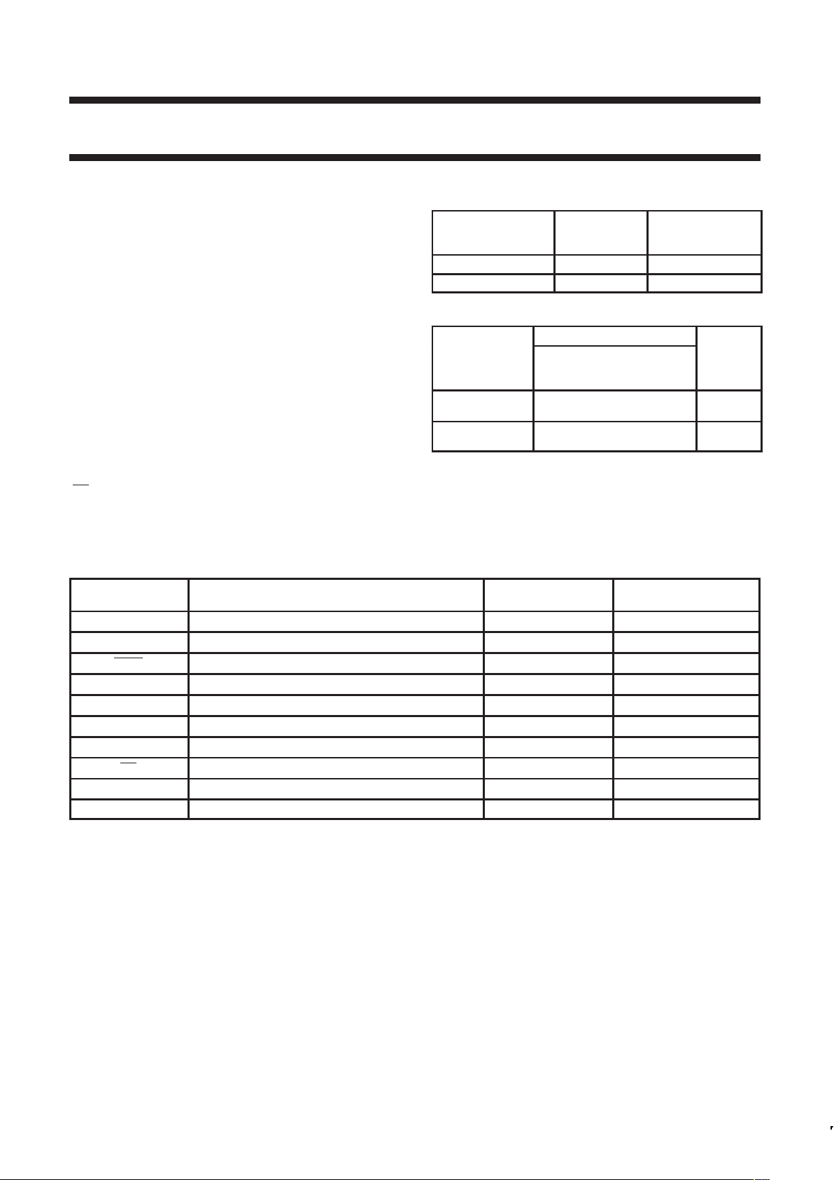
PIN CONFIGURATION – 74ALS646/646-1
1
2
3
4
5
6
7
8
9
10
11
12 13
14
15
16
17
18
19
20
21
22
23
24
CPAB
SAB
DIR
A0
A1
A2
A3
A4
A5
A6
A7
V
CC
CPBA
SBA
OE
B0
B1
B2
B4
B3
B5
B6
B7
GND
SC00118
PIN CONFIGURATION – 74ALS648/648-1
1
2
3
4
5
6
7
8
9
10
11
12 13
14
15
16
17
18
19
20
21
22
23
24
CPAB
SAB
DIR
A0
A1
A2
A3
A4
A5
A6
A7
V
CC
CPBA
SBA
OE
B0
B
1
B
2
B
4
B3
B
5
B
6
B
7
GND
SC00119
LOGIC SYMBOL – 74ALS646/646-1
B0 B1 B2 B3 B4 B5 B6 B7
A0 A1 A2 A3 A4 A5 A6 A7
4567891011
20 19 18 17 16 15 14 13
V
CC
= Pin 24
GND = Pin 12
SC00120
CPAB
SAB
DIR
SPBA
SBA
OE
1
2
3
23
22
21
LOGIC SYMBOL – 74ALS648/648-1
B0 B1 B2 B3 B4 B5 B6 B7
A0 A1 A2 A3 A4 A5 A6 A7
4567891011
20 19 18 17 16 15 14 13
VCC = Pin 24
GND = Pin 12
SC00121
CPAB
SAB
DIR
SPBA
SBA
OE
1
2
3
23
22
21
IEC/IEEE SYMBOL – 74ALS646/646-1
2
1
C4
G5
G7
C6
20
7
5
6D
4D
1
1
1
1
4
21
SC00122
G3
3 EN1 [BA]
3 EN2 [AB]
3
23
22
1
2
5
6
7
8
9
10
11
19
18
17
16
15
14
13
5
7
IEC/IEEE SYMBOL – 74ALS648/648-1
2
1
C4
G5
G7
C6
20
7
5
6D
4D
1
1
1
1
4
21
SC00123
G3
3 EN1 [BA]
3 EN2 [AB]
3
23
22
1
2
5
6
7
8
9
10
11
19
18
17
16
15
14
13
5
7
Page 4
Philips Semiconductors Product specification
74ALS646/74ALS646-1
74ALS648/74ALS648-1
Transceiver/register
1991 Feb 08
4
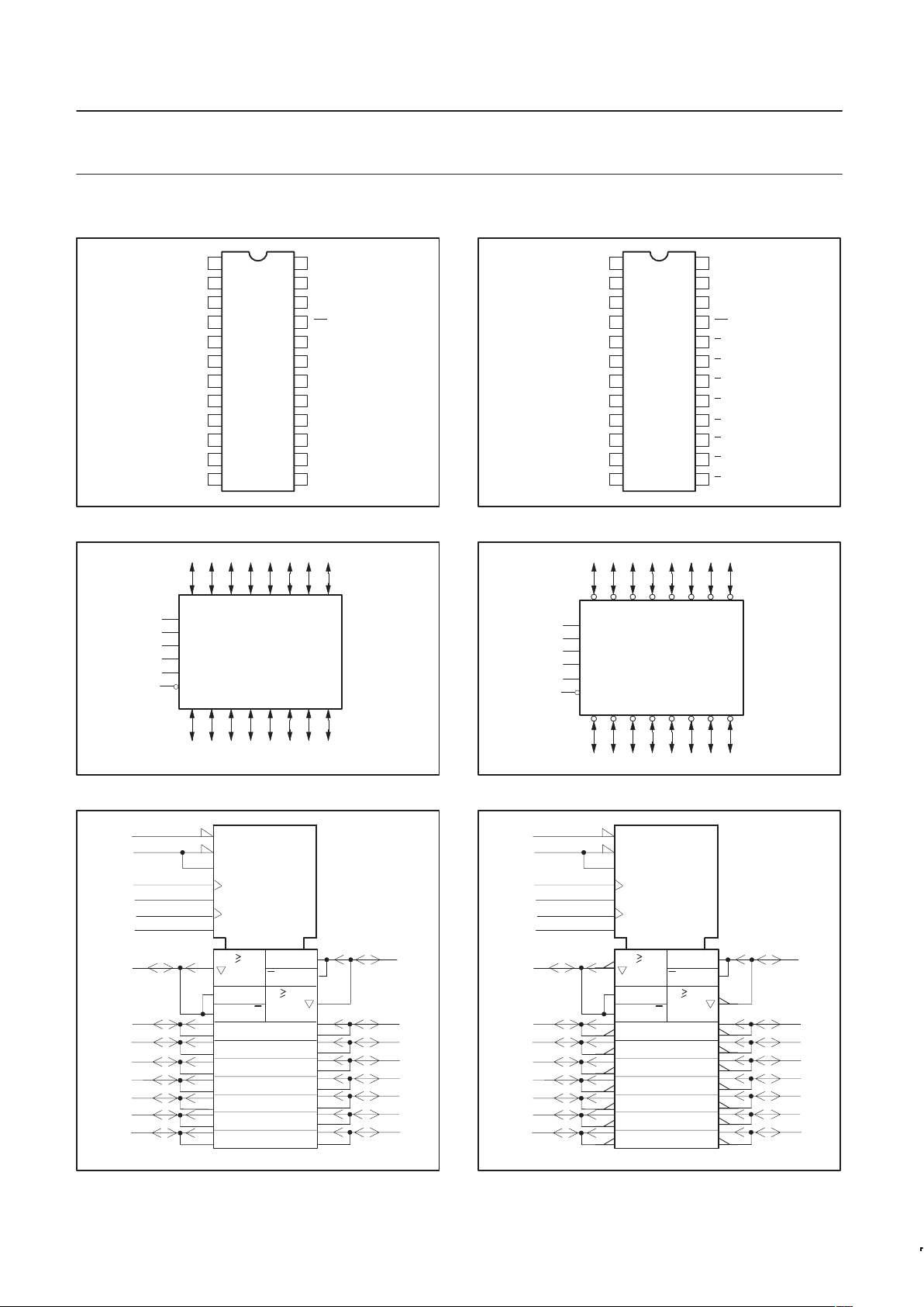
BUS MANAGEMENT FUNCTIONS
The following examples demonstrate the four fundamental
bus-management functions that can be performed with the
74ALS646/646-1 and 74ALS648/648-1.
The select pins determine whether data is stored or transferred
through the device in real time.
The DIR determines which bus will receive data when the OE pin is
Low.
REAL TIME BUS TRANSFER
BUS B TO BUS A
REAL TIME BUS TRANSFER
BUS A TO BUS B
STORAGE FROM
A, B, OR A AND B
TRANSFER STORED DATA
TO A AND/OR B
OE DIR CPABCPBA SAB SBA
LL X X X L
BUS A
BUS A BUS A
BUS A BUS BBUS BBUS B
BUS B
OE
DIR CPABCPBA SAB SBA
LH X X L X
OE DIR CPABCPBA SAB SBA
XX ↑ XXX
XX X ↑ XX
HX ↑↑XX
OE
DIR CPABCPBA SAB SBA
L L X H or L X H
L H H or L X H X
SF00392
Page 5

Philips Semiconductors Product specification
74ALS646/74ALS646-1
74ALS648/74ALS648-1
Transceiver/register
1991 Feb 08
5
LOGIC SYMBOL – 74ALS646/646-1
V
CC
= Pin 24
GND = Pin 12
A0
OE
B0
1D
C1
1D
C1
DIR
CPBA
SBA
CPAB
SAB
1 OF 8 CHANNELS
TO 7 OTHER CHANNELS
21
4
20
3
23
22
1
2
SC00124
LOGIC SYMBOL – 74ALS648/648-1
V
CC
= Pin 24
GND = Pin 12
A0
OE
B0
1D
C1
1D
C1
DIR
CPBA
SBA
CPAB
SAB
1 OF 8 CHANNELS
TO 7 OTHER CHANNELS
21
4
20
3
23
22
1
2
SC00125
FUNCTION TABLE
INPUTS DATA I/O OPERATING MODE
OE DIR CPAB CPBA SAB SBA An Bn 74ALS646/74ALS646-1 74ALS648/74ALS648-1
X X ↑ X X X Input Unspecified* Store A, B unspecified* Store A, B unspecified*
X X X ↑ X X Unspecified* Input Store B, A unspecified* Store B, A unspecified*
H X ↑ ↑ X X Input Input Store A and B data Store A and B data
H X H or L H or L X X Input Input Isolation, hold storage Isolation, hold storage
L L X X X L Output Input Real time B data to A bus Real time B data to A bus
L L X H or L X H Output Input Stored B data to A bus Stored B data to A bus
L H X X L X Input Output Real time A data to B bus Real time A data to B bus
L H H or L X H X Input Output Stored A data to B bus Stored A data to B bus
NOTES:
H = High voltage level
L = Low voltage level
X = Don’t care
* = The data output function may be enabled or disabled by various signals at the OE
and DIR inputs. Data input functions are always
enabled, i.e., data at the bus pins will be stored on every Low-to-High transition of the clock.
↑ = Low-to-High clock transition
Page 6

Philips Semiconductors Product specification
74ALS646/74ALS646-1
74ALS648/74ALS648-1
Transceiver/register
1991 Feb 08
6
ABSOLUTE MAXIMUM RATINGS
(Operation beyond the limit set forth in this table may impair the useful life of the device.
Unless otherwise noted these limits are over the operating free-air temperature range.)
SYMBOL
PARAMETER RATING UNIT
V
CC
Supply voltage –0.5 to +7.0 V
V
IN
Input voltage –0.5 to +7.0 V
I
IN
Input current –30 to +5 mA
V
OUT
Voltage applied to output in High output state –0.5 to V
CC
V
pp
p
p
All versions 48 mA
I
OUT
Current applied to output in Low output state
-1 version 96 mA
T
amb
Operating free-air temperature range 0 to +70 °C
T
stg
Storage temperature range –65 to +150 °C
RECOMMENDED OPERATING CONDITIONS
PARAMETER
LIMITS
SYMBOL
MIN NOM MAX
UNIT
V
CC
Supply voltage 4.5 5.0 5.5 V
V
IH
High-level input voltage 2.0 V
V
IL
Low-level input voltage 0.8 V
I
IK
Input clamp current –18 mA
I
OH
High-level output current –15 mA
p
All versions 24 mA
IOLLow-level output current
-1 version 48
1
mA
T
amb
Operating free-air temperature range 0 +70 °C
NOTE:
1. The 48mA limit applies only under the condition of V
CC
= 5.0V ±5%.
Page 7

Philips Semiconductors Product specification
74ALS646/74ALS646-1
74ALS648/74ALS648-1
Transceiver/register
1991 Feb 08
7
DC ELECTRICAL CHARACTERISTICS
(Over recommended operating free-air temperature range unless otherwise noted.)
LIMITS
SYMBOL
PARAMETER
TEST CONDITIONS
1
MIN TYP
2
MAX
UNIT
VCC±10%, VIL = MAX,
IOH = –0.4mA V
CC
– 2 V
-
p
CC
,
IL
,
VIH = MIN
IOH = –3mA 2.4 3.2 V
VOHHigh level out ut voltage
VCC = MIN, VIL = MAX,
V
IH
= MIN
IOH = –15mA 2.0 V
VCC = MIN, VIL = MAX,
I
OL
= 12mA 0.25 0.40 V
-
p
All versions
CC
,
IL
,
VIH = MIN
I
OL
= 24mA 0.35 0.50 V
VOLLow level out ut voltage
-1 versions
VCC = 4.75V , VIL = MAX,
V
IH
= MIN
I
OL
= 48mA 0.35 0.50 V
V
IK
Input clamp voltage VCC = MIN, II = I
IK
–0.73 –1.5 V
Input current at maxi-
control inputs VCC = MAX, VI = 7.0V 0.1 mA
I
I
mum input voltage
A or B ports VCC = MAX, VI = 5.5V 0.1 mA
I
IH
High-level input current
3
VCC = MAX, VI = 2.7V 20 µA
I
IL
Low-level input current
3
VCC = MAX, VI = 0.4V –0.1 mA
I
O
Output current
4
VCC = MAX, VO = 2.25V –30 –112 mA
I
CCH
40 57 mA
I
CC
Supply current (total)
I
CCL
VCC = MAX
53 78 mA
I
CCZ
51 72 mA
NOTES:
1. For conditions shown as MIN or MAX, use the appropriate value specified under recommended operating conditions for the applicable type.
2. All typical values are at V
CC
= 5V, T
amb
= 25°C.
3. For I/O ports, the parameter I
IH
and IIL include the off-state current.
4. The output conditions have been chosen to produce a current that closely approximates one half of the true short-circuit output current, I
OS
.
AC ELECTRICAL CHARACTERISTICS FOR 74ALS646/74ALS646-1
LIMITS
SYMBOL PARAMETER TEST CONDITION
T
amb
= 0°C to +70°C
V
CC
= +5.0V ± 10%
C
L
= 50pF, RL = 500Ω
UNIT
MIN MAX
f
max
Maximum clock frequency Waveform 1 100 MHz
t
PLH
t
PHL
Propagation delay
CPBA to An, CPAB to Bn
Waveform 1
5.0
6.0
13.0
13.0
ns
t
PLH
t
PHL
Propagation delay
An to Bn or Bn to An
Waveform 2, 3
2.0
3.0
8.0
9.0
ns
t
PLH
t
PHL
Propagation delay
SBA to An or SAB to Bn (A or B Low)
Waveform 2, 3
5.0
5.0
13.0
11.0
ns
t
PLH
t
PHL
Propagation delay
SBA to An or SAB to Bn (A or B High)
Waveform 2, 3
5.0
5.0
11.0
11.0
ns
t
PZH
t
PZL
Output enable time
OE
to An or Bn
Waveform 5
Waveform 6
3.0
5.0
9.0
11.0
ns
t
PHZ
t
PLZ
Output disable time
OE
to An or Bn
Waveform 5
Waveform 6
2.0
3.0
8.0
10.0
ns
t
PZH
t
PZL
Output enable time
DIR to An or Bn
Waveform 5
Waveform 6
2.0
5.0
10.0
12.0
ns
t
PHZ
t
PLZ
Output disable time
DIR to An or Bn
Waveform 5
Waveform 6
2.0
3.0
10.0
13.0
ns
Page 8

Philips Semiconductors Product specification
74ALS646/74ALS646-1
74ALS648/74ALS648-1
Transceiver/register
1991 Feb 08
8
AC ELECTRICAL CHARACTERISTICS FOR 74ALS648/74ALS648-1
LIMITS
SYMBOL PARAMETER TEST CONDITION
T
amb
= 0°C to +70°C
V
CC
= +5.0V ± 10%
C
L
= 50pF, RL = 500Ω
UNIT
MIN MAX
f
max
Maximum clock frequency Waveform 1 100 MHz
t
PLH
t
PHL
Propagation delay
CPBA to An, CPAB to Bn
Waveform 1
5.0
6.0
13.0
13.0
ns
t
PLH
t
PHL
Propagation delay
An to Bn or Bn to An
Waveform 2, 3
1.0
3.0
7.0
9.0
ns
t
PLH
t
PHL
Propagation delay
SBA to An or SAB to Bn (A or B Low)
Waveform 2, 3
5.0
5.0
13.0
11.0
ns
t
PLH
t
PHL
Propagation delay
SBA to An or SAB to Bn (A or B High)
Waveform 2, 3
4.0
5.0
11.0
11.0
ns
t
PZH
t
PZL
Output enable time
OE
to An or Bn
Waveform 5
Waveform 6
2.0
4.0
8.0
13.0
ns
t
PHZ
t
PLZ
Output disable time
OE
to An or Bn
Waveform 5
Waveform 6
1.0
2.0
8.0
10.0
ns
t
PZH
t
PZL
Output enable time
DIR to An or Bn
Waveform 5
Waveform 6
3.0
5.0
10.0
12.0
ns
t
PHZ
t
PLZ
Output disable time
DIR to An or Bn
Waveform 5
Waveform 6
2.0
2.0
11.0
11.0
ns
AC SETUP REQUIREMENTS
LIMITS
SYMBOL PARAMETER TEST CONDITION
T
amb
= 0°C to +70°C
V
CC
= +5.0V ± 10%
C
L
= 50pF, RL = 500Ω
UNIT
t
su
(H)
t
su
(L)
Setup time, High or Low
An or Bn to CPAB or CPBA
Waveform 4
5.0
5.0
ns
t
h
(H)
t
h
(L)
Hold time, High or Low
An or Bn to CPAB or CPBA
Waveform 4
0.0
1.0
ns
t
w
(H)
t
w
(L)
Pulse width, High or Low
CPAB or CPBA
Waveform 1
6.0
4.0
ns
Page 9

Philips Semiconductors Product specification
74ALS646/74ALS646-1
74ALS648/74ALS648-1
Transceiver/register
1991 Feb 08
9
AC WAVEFORMS
For all waveforms, VM = 1.3V .
The shaded areas indicate when the input is permitted to change for predictable output performance.
CPBA
or
CPAB
V
M
V
M
V
M
tw(H)
1/f
max
V
M
V
M
t
PLH
tw(L)
t
PHL
An or Bn
SF00394
Waveform 1. Propagation Delay for Clock Input to Output,
Clock Pulse Width, and Maximum Clock Frequency
SF00395
V
M
V
M
V
M
V
M
Bn or An
An or Bn
t
PLH
t
PHL
SBA or SAB
An or Bn
Waveform 2. Propagation Delay for An to Bn or Bn to An
and SAB or SBA to An or Bn
V
M
V
M
V
M
V
M
t
PHL
t
PLH
An or Bn
Bn or An
SBA or SAB
An or Bn
SF00396
Waveform 3. Propagation Delay for An to Bn or Bn to An
and SAB or SBA to An or Bn
V
M
V
M
V
M
V
M
V
M
V
M
tsu(L) th(L)
t
su
(H) th(H)
An or Bn
CPBA
or
CPAB
SF00397
Waveform 4. Data Setup Time and Hold Times
V
M
V
M
V
M
t
PHZ
t
PZH
OE
VOH -0.3V
0V
An or Bn
DIR
SF00398
Waveform 5. 3-State Output Enable Time to High Level
and Output Disable Time from High Level
V
M
V
M
V
M
t
PLZ
t
PZL
VOL +0.3V
3.5V
OE
DIR
An or Bn
SF00399
Waveform 6. 3-State Output Enable Time to Low Level
and Output Disable Time from Low Level
Page 10

Philips Semiconductors Product specification
74ALS646/74ALS646-1
74ALS648/74ALS648-1
Transceiver/register
1991 Feb 08
10
TEST CIRCUIT AND WAVEFORMS
t
w
90%
V
M
10%
90%
V
M
10%
90%
V
M
10%
90%
V
M
10%
NEGATIVE
PULSE
POSITIVE
PULSE
t
w
AMP (V)
0.3V
0.3V
t
THL (tf
f
)
INPUT PULSE REQUIREMENTS
Rep.Rate
t
w
t
TLHtTHL
1MHz
500ns
2.0ns 2.0ns
Input Pulse Definition
V
CC
Family
74ALS
D.U.T.
PULSE
GENERATOR
R
L
C
L
R
T
V
IN
V
OUT
Test Circuit for 3-State and Open Collector Outputs
DEFINITIONS:
R
L
= Load resistor;
see AC electrical characteristics for value.
CL= Load capacitance includes jig and probe capacitance;
see AC electrical characteristics for value.
R
T
= Termination resistance should be equal to Z
OUT
of
pulse generators.
t
THL (tf
)
t
TLH (tr
)
t
TLH (tr
)
AMP (V)
Amplitude
3.5V
1.3V
V
M
SC00126
R
L
7.0V
SWITCH POSITION
TEST SWITCH
t
PLZ
, t
PZL
closed
open collector closed
All other open
Page 11

Transceiver/register
Philips Semiconductors Product specification
74ALS646/74ALS646–1
74ALS648/74ALS648–1
1991 Feb 08
11
DIP24: plastic dual in-line package; 24 leads (300 mil) SOT222-1
Page 12

Transceiver/register
Philips Semiconductors Product specification
74ALS646/74ALS646–1
74ALS648/74ALS648–1
1991 Feb 08
12
SO24: plastic small outline package; 24 leads; body width 7.5 mm SOT137-1
Page 13

Transceiver/register
Philips Semiconductors Product specification
74ALS646/74ALS646–1
74ALS648/74ALS648–1
1991 Feb 08
13
Philips Semiconductors and Philips Electronics North America Corporation reserve the right to make changes, without notice, in the products,
including circuits, standard cells, and/or software, described or contained herein in order to improve design and/or performance. Philips
Semiconductors assumes no responsibility or liability for the use of any of these products, conveys no license or title under any patent, copyright,
or mask work right to these products, and makes no representations or warranties that these products are free from patent, copyright, or mask
work right infringement, unless otherwise specified. Applications that are described herein for any of these products are for illustrative purposes
only. Philips Semiconductors makes no representation or warranty that such applications will be suitable for the specified use without further testing
or modification.
LIFE SUPPORT APPLICA TIONS
Philips Semiconductors and Philips Electronics North America Corporation Products are not designed for use in life support appliances, devices,
or systems where malfunction of a Philips Semiconductors and Philips Electronics North America Corporation Product can reasonably be expected
to result in a personal injury. Philips Semiconductors and Philips Electronics North America Corporation customers using or selling Philips
Semiconductors and Philips Electronics North America Corporation Products for use in such applications do so at their own risk and agree to fully
indemnify Philips Semiconductors and Philips Electronics North America Corporation for any damages resulting from such improper use or sale.
This data sheet contains preliminary data, and supplementary data will be published at a later date. Philips
Semiconductors reserves the right to make changes at any time without notice in order to improve design
and supply the best possible product.
Philips Semiconductors
811 East Arques Avenue
P.O. Box 3409
Sunnyvale, California 94088–3409
Telephone 800-234-7381
DEFINITIONS
Data Sheet Identification Product Status Definition
Objective Specification
Preliminary Specification
Product Specification
Formative or in Design
Preproduction Product
Full Production
This data sheet contains the design target or goal specifications for product development. Specifications
may change in any manner without notice.
This data sheet contains Final Specifications. Philips Semiconductors reserves the right to make changes
at any time without notice, in order to improve design and supply the best possible product.
Copyright Philips Electronics North America Corporation 1997
All rights reserved. Printed in U.S.A.
 Loading...