

Page 1
EB-CCD
TAPPB0068EA
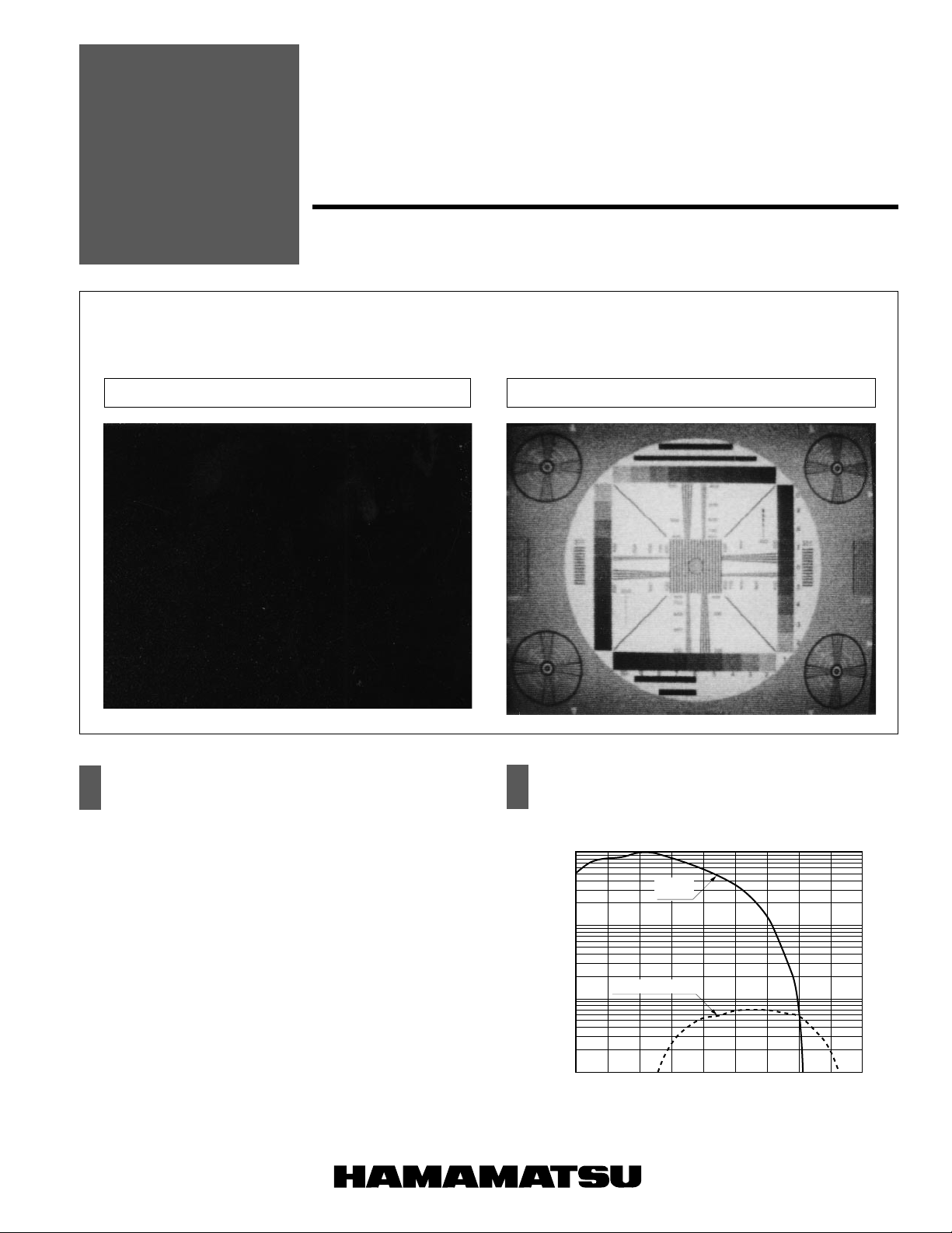
SENSITIVITY (V
.
µJ
-1
.
cm
-2
)
200
1
10
100
1000
300 400 500 600 700 800 900 1000 1100
EB-CCD
N7640
NORMAL 2/3" CCD
WAVELENGTH (nm)
TV SCAN RATE TYPE : N7640
SLOW SCAN TYPE : N7220
PRELIMINARY
For Low-Light-Level Imaging with high S/N ratio
IMAGING COMPARISON
Using Resolution Test Chart
Commercial 2/3-inch CCD
■ Imaging Conditions
Object illuminance: 0.1 lx
Lens: FUJINON-TV Zoom Lens/H6x 12.5R :F1.2/f2
EB-CCD N7640
OVERVIEW
The EB-CCD is an absolutely new high-sensitivity imaging
device that employs the “Electron Bombardment (EB)” effect for
image intensification. The EB-CCD basically consists of a
photocathode and a CCD chip arranged in parallel in a vacuum
tube. An optical image is converted at the photocathode into an
electron image, which is then accelerated and directly bombards the CCD surface to produce electron multiplication. Even
a low-light-level image can be brought into view with a high S/N
ratio.
Two types of EB-CCD are available depending on the readout
method: the N7640 designed to operate at the TV scan rate
and the N7220 for slow scan readout. Both types are compact
and simple in structure, and deliver high sensitivity yet ensure
high S/N ratio. The EB-CCD will open up new applications as
the next generation of low-light-level imaging devices.
SENSITIVITY COMPARISON
(Calculated data)
Page 2
APPLICATIONS
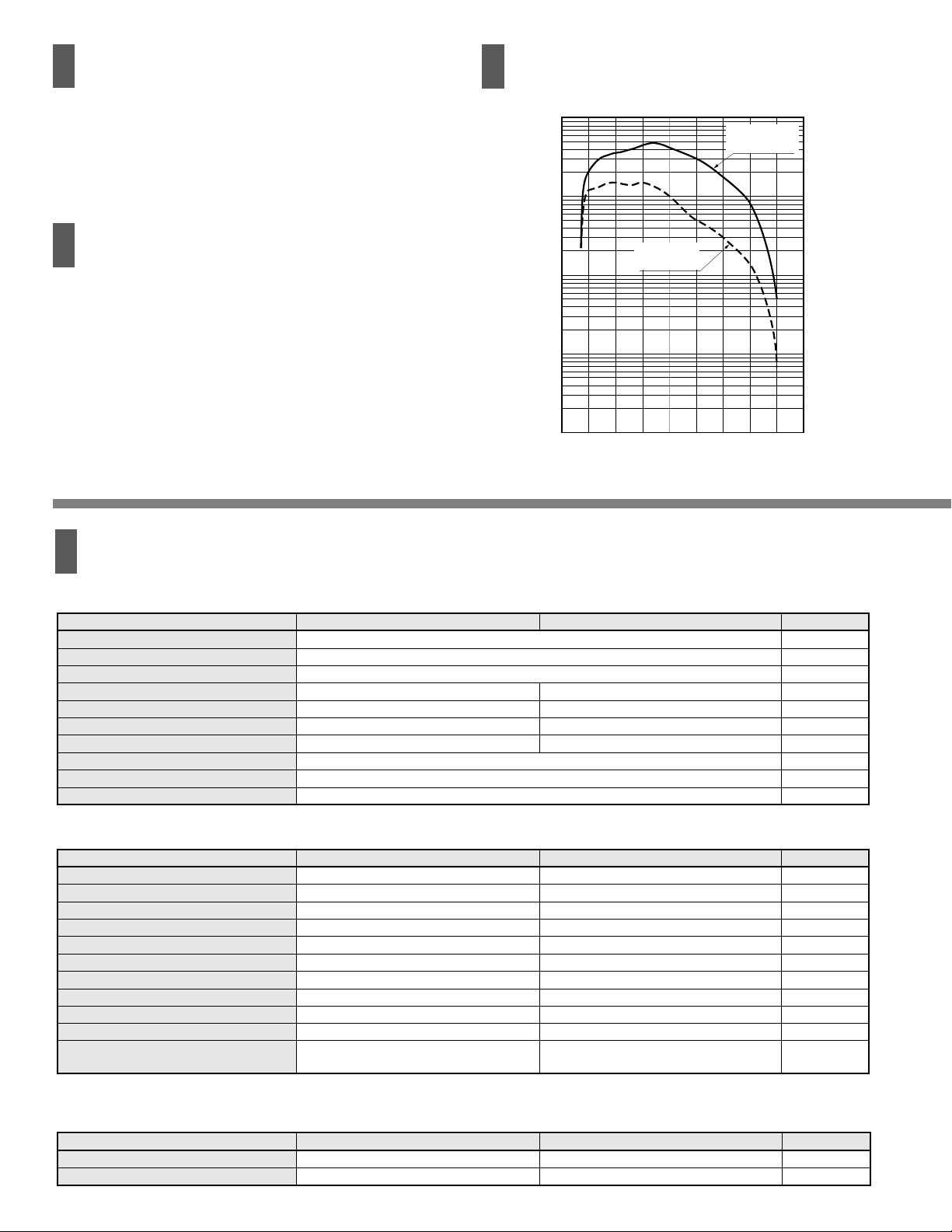
SPECTRAL RESPONSE
●High sensitivity video camera
• Semiconductor wafer inspection
• Real time fluorescence observation
• Biochemical emission imaging
• Biophoton imaging
FEATURES
TV scan rate type
●Resolution 400 TV lines
●Gain 700
●Detection limit
*1
0.3 mlx
Slow scan type
●Resolution 450 TV lines
●Gain 1300
●Detection limit Detectable down to single photon
region
*1: Minimum illuminance on the photocathode required to produce an image.
SPECIFICATIONS
TII B0020EA
2
10
1
10
QUANTUM
0
10
QUANTUM EFFICIENCY (%)
-1
10
CATHODE RADIANT SENSITIVITY (mA/W)
-2
10
100 200 300 400 500 600 700
EFFICIENCY
WAVELENGTH (nm)
CATHODE
SENSITIVITY
800 900
1000
●EB-CCD
Parameter
Focusing Method
Window Material
Photocathode
Maximum Supply Voltage
Gain
Limiting Resolution
Effective Area (H✕V)
Casing Material
Lead Wire Sheath
Dimension
*2: N7640
*2
(Typ.)
(Typ.)
at -6 kV, N7220 at -8 kV
9.2 ✕ 6.8
●Internal CCD
Parameter
Drive Method
CCD Format
Pixel Size
Number of Effective Pixels (H✕V)
Saturation Charge
Dark Current
Readout Noise
CCD Readout Frequency
Vertical Clock
Horizontal Clock
Output
*3: At 25 °C, MPP (Multi-Pinned Phase) operation, 33 ms/frame
*4: At 0 °C, MPP (Multi-Pinned Phase) operation
*5
MOSFET source follower, two stages
Frame transfer
2/3 inch format
658 ✕ 490
*3
80 e- / (pixel·frame)
2 phases
2 phases
with load
●Ratings
Parameter
Operating Temperature Range
Storage Temperature Range
N7640 N7220
Proximity-focused
Synthetic silica
Multialkali
-6
700
400
Poly Oxy Methylene (POM)
Teflon
φ53 ✕ 16.5 (excluding lead pins)
N7640 N7220 Unit
Full frame transfer
14 ✕ 14
3
65 ✕10
100
14
MOSFET source follower, one stage
*5: N7640 at 12 MHz, N7220 at 150 kHz
Min. Max.
-30
-40
*4
-8
1300
450
12.2 ✕ 12.2
1 inch format
24 ✕ 24
512 ✕ 512
200 ✕10
300 e- / (pixel·s)
2 phases
2 phases
3
50
1
+40
+40
Unit
kV
TV lines
mm
mm
mm
electrons
e- RMS
MHz
Unit
-
-
-
-
-
-
-
-
-
-
-
-
-
°C
°C
Page 3
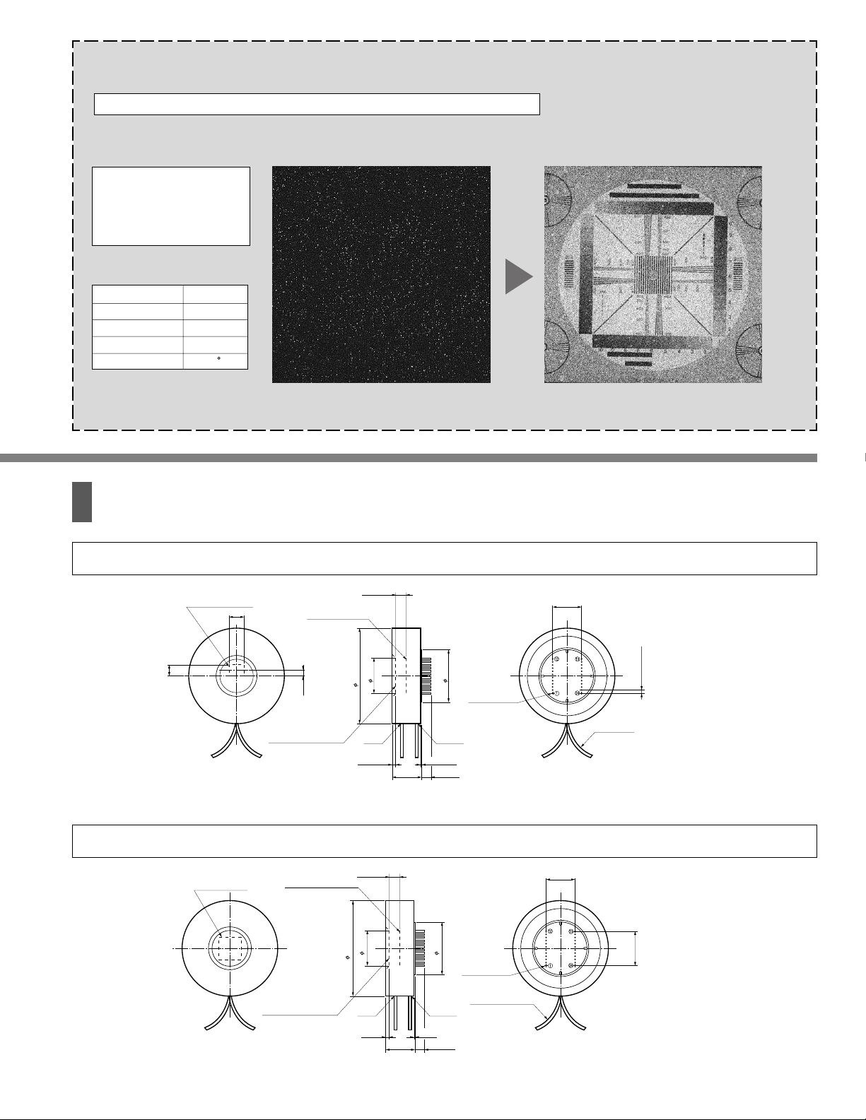
PHOTON COUNTING IMAGING EXAMPLE
Slow Scan Type N7220
Exposure Time: 0.02 s Exposure Time: 20 s
Object Illuminance
0.00002 lx
●Conditions
Light source
Object illuminance
Lens F value
Supply voltage
Ambient temperature
Tungsten lamp
-5
2✕10
lx
5.6
-8 kV
-25 C
(Resolution 450 TV lines)
DIMENSIONAL OUTLINES (Unit: mm)
TV Rate Type (Frame Transfer CCD) N7640
EFFECTIVE
IMAGING AREA
9.2(H)✕6.8(V) MIN.
6.8
LEAD (TEFLON COVER)
RED : PHOTOCATHODE (–HV)
BLACK : OUTER FLANGE (GND)
9.2
Input Side
PHOTOCATHODE
(MULTIALKALI)
3.57
INPUT WINDOW
(SYNTHETIC SILICA)
Slow Scan Type (Full Frame Transfer CCD) N7220
EFFECTIVE
IMAGING AREA
12.2✕12.2 MIN.
PHOTOCATHODE
(MULTIALKALI)
6.9 ± 0.1
+0
53-0.3
2.0 ± 0.3
5.9±0.1
19
16.5 ± 0.3
BLACKRED
0.5 ± 0.2
5 ± 0.3
29
INDEX MARK
15.2 ± 0.2
Output Side
15.2±0.2
1.78 ± 0.15
CABLE LENGTH
200 MIN.
TAPPA0037EA
INPUT WINDOW
(SYNTHETIC SILICA)
Input Side
LEAD (TEFLON COVER)
RED : PHOTOCATHODE (–HV)
BLACK : OUTER FLANGE (GND)
+0
19
53–0.3
2±0.2
16.5 ± 0.3
29
BLACKRED
0.5 ± 0.2
5 ± 0.3
INDEX MARK
CABLE LENGTH
200 MIN.
Output Side
=19.6
1.78×11
TAPPA0034ED
Page 4
EB-CCD
The C8080 is an EB-CCD camera incorporating a TV scan type EB-CCD (N7640). The
C8080 is designed for simple use and functions, yet capable of imaging at very low
CAMERA
C8080
light levels. Hamamatsu also provides the C8081 power supply ideal for use with the
C8080 EB-CCD camera.
●SPECIFICATIONS
Parameter
EB-CCD
Image Sensor
Spectral Response
Gain
Effective Area
8.58 ✕ 6.86 (2/3 inch format)
Number of Effective Pixels (H ✕ V)
Pixel Size
Saturation Charge
Frame Rate
Image Output Method
Operating Temperature Range
Storage Temperature Range
Humidity Range
Input Voltage
(Input Current)
Below 90 (no condensation)
(500 mA)
+15
Dimension (W ✕ H ✕ D)
Weight
●DEDICATED POWER SUPPLY C8081 (Option)
Parameter
Input Voltage
Maximum Power Consumption
Dimension (W ✕ H ✕ D)
Weight
Specifications
EB-CCD (N7640)
Frame transfer CCD
185 to 900
200 to 700
640 ✕ 480
14 ✕ 14
130 000
60 Hz interlace
RS-170 (EIA)
0 to +40
-10 to +40
, -15
(500 mA)
, +5
90 ✕ 75 ✕ 160
Approx. 1.4
Specifications
85 to 135 (50 Hz, 60 Hz)
90
161 ✕ 44 ✕ 213
Approx. 1.2
(500 mA)
Unit
-
-
nm
-
mm
-
µm
electrons
-
-
°C
°C
%
V
mm
kg
Unit
V ac
VA
mm
kg
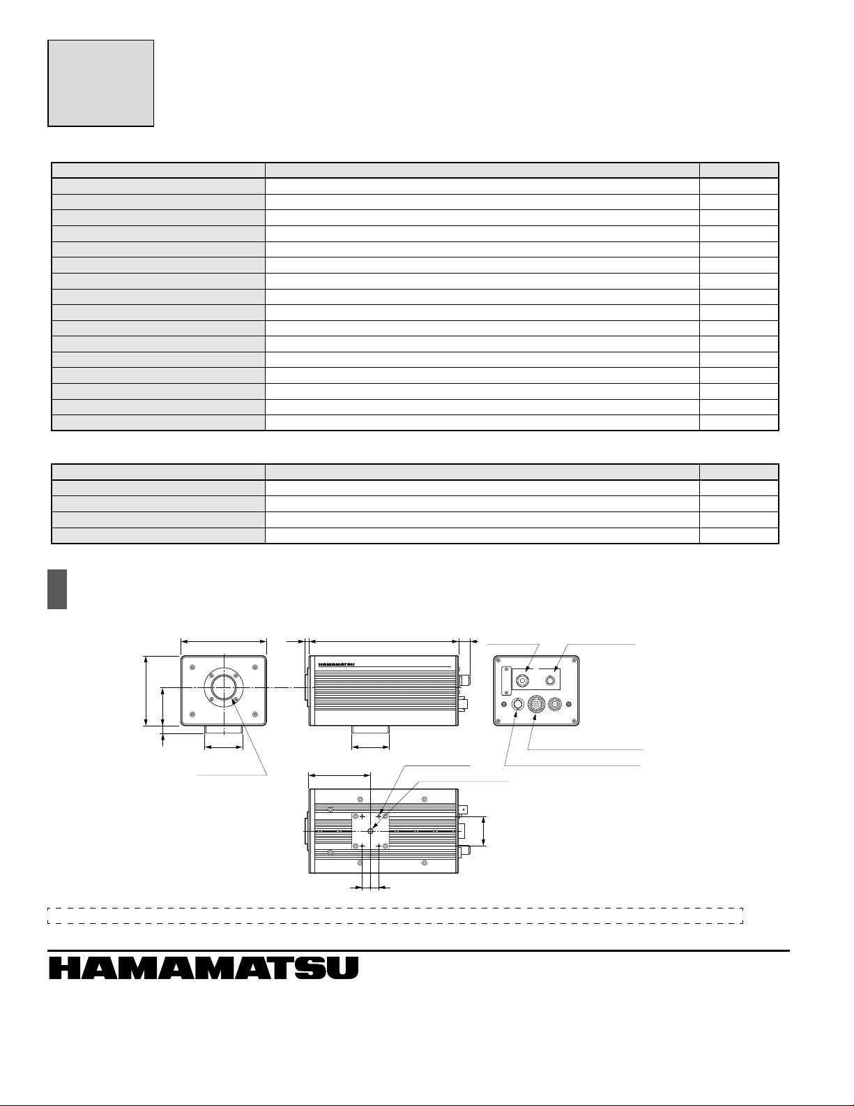
DIMENSIONAL OUTLINES (Unit: mm)
● C8080
75
418
Subject to local technical requirements and regulations, availability of products in this promotional material may vary. Please consult with our sales office.
Information furnished by HAMAMATSU is believed to be reliable. However, no responsibility is assumed for possible inaccuracies and omissions.
Specifications are subject to change without notice. No patent rights are granted to any of the circuits described herein. © 2000 Hamamatsu Photonics K.K.
HAMAMATSU PHOTONICS K.K., Electron Tube Center
314-5, Shimokanzo, Toyooka-village, Iwata-gun, Shizuoka-ken, 438-0193, Japan, Telephone: (81)539/62-5248, Fax: (81)539/62-2205
U.S.A.:
Hamamatsu Corporation: 360 Foothill Road, P. O. Box 6910, Bridgewater. N.J. 08807-0910, U.S.A., Telephone: (1)908-231-0960, Fax: (1)908-231-1218 E-mail: [email protected]
Germany:
Hamamatsu Photonics Deutschland GmbH: Arzbergerstr. 10, D-82211 Herrsching am Ammersee, Germany, Telephone: (49)8152-375-0, Fax: (49)8152-2658 E-mail: [email protected]
France:
Hamamatsu Photonics France S.A.R.L.: 8, Rue du Saule Trapu, Parc du Moulin de Massy, 91882 Massy Cedex, France, Telephone: (33)1 69 53 71 00, Fax: (33)1 69 53 71 10 E-mail: [email protected]
United Kingdom:
North Europe:
Italy:
Hamamatsu Photonics UK Limited: 2 Howard Court, 10 Tewin Road Welwyn Garden City Hertfordshire AL7 1BW, United Kingdom, Telephone: 44-(0)1707-294888, Fax: 44(0)1707-325777 E-mail: [email protected]
Hamamatsu Photonics Norden AB: Smidesvägen 12, SE-171-41 SOLNA, Sweden, Telephone: (46)8-509-031-00, Fax: (46)8-509-031-01 E-mail: [email protected]
Hamamatsu Photonics Italia: S.R.L.: Strada della Moia, 1/E, 20020 Arese, (Milano), Italy, Telephone: (39)02-935 81 733, Fax: (39)02-935 81 741 E-mail: [email protected]
90
C MOUNT
DEPTH: 6
160 124.1
EB-CCD CAMERA
4040
66
99
HOMEPAGE URL http://www.hamamatsu.com
C8080
4-M3, DEPTH: 8
1/4-20 UNC, DEPTH: 8
32
GAIN CONTROLH.V. SWITCH
HV
SENSITIVITYON/OFF
MIN. MAX.
VIDEO
CONTROL
POWER
POWER INPUT
(HIROSE HR10A-R13R-20SB)
VIDEO SIGNAL OUTPUT (BNC)
TAPPA0041EA
TAPP1032E01
OCT. 2000 (9910) IP
Printed in Japan (1000)
 Loading...