

Page 1
NIKO-SEM
1.5 MHz, 600mA Synchronous
Step-Down Converter
N6200
SOT-25
Lead-Free
GENERAL DESCRIPTION
N6200 is a 1.5Mhz constant frequency, slope compensated current mode PWM step-down converter. The
device integrates a main switch and a synchronous rectifier for high efficiency without an external Schottky
diode. It is ideal for powering portable equipment that runs from a single cell lithium-Ion (Li+) battery. The
N6200 can supply 600mA of load current from a 2.5V to 5.5V input voltage. The output voltage can be
regulated as low as 0.6V. The N6200 can also run at 100% duty cycle for low dropout operation, extending
battery life in portable system. Idle mode operation at light loads provides very low output ripple voltage for
noise sensitive applications.
The N6200 is offered in a low profile (1mm) 5-pin, thin SOT package, and is available in an adjustable
version and fixed output voltage of 1.2V, 1.5V and 1.8V.
APPLICATIONS
‧ Cellular and Smart Phones
‧ Microprocessors and DSP Core Supplies
‧ Wireless and DSL Modems
‧ PDAs
FEATURES
‧ High Efficiency: Up to 92%
‧ 1.5Mhz Constant Switching Frequency
‧ 600mA Output Current at V
‧ Integrated Main switch and synchronous
rectifier. No Schottky Diode Required
‧ 2.5V to 5.5V Input Voltage Range
‧ Output Voltage as Low as 0.6V
‧ 100% Duty Cycle in Dropout
IN
= 3V
‧ MP3 Player
‧ Digital Still and Video Cameras
‧ Portable Instruments
‧ Low Quiescent Current : 300µA
Slope Compensated ‧ Current Mode Control for
Excellent Line and Load Transient Response
Short Circuit Protection‧
Thermal Fault Protection‧
‧ <1uA Shutdown Current
‧Space Saving 5-Pin SOT-25 package
1
May-8-2006
Page 2
NIKO-SEM
1.5 MHz, 600mA Synchronous
Step-Down Converter
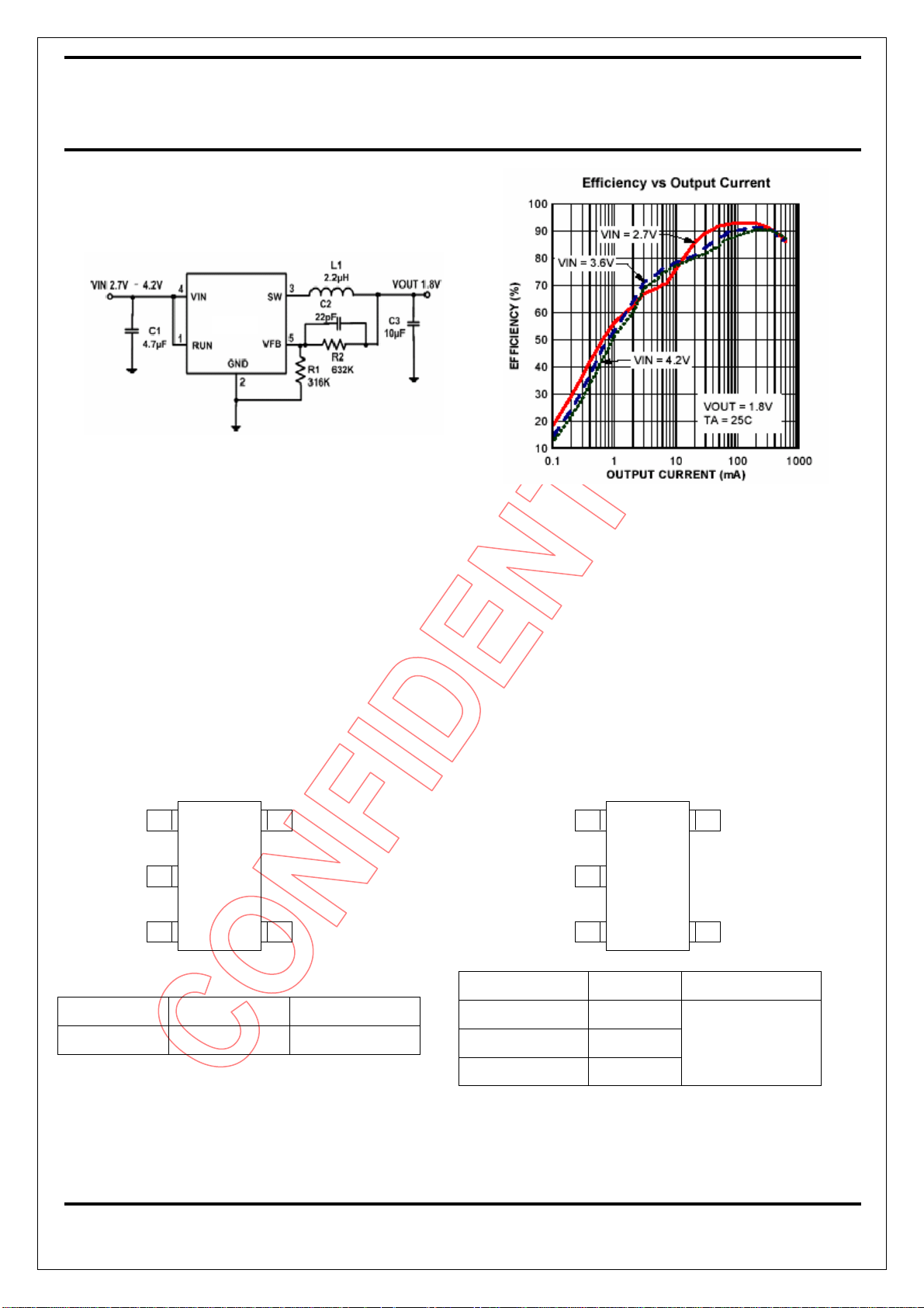
Typical Application
N6200
Figure 1 Basic Application Circuit with N6200
adjustable version, Vout = 1.8V
N6200
SOT-25
Lead-Free
Absolute Maximum Rating
Input Supply Voltage............................ -0.3V to +6V
RUN, V
SW, V
Peak SW Sink and Source Current ......................1.5A
Voltages ............................ -0.3V to VIN+0.3V
FB
Voltages...............................-0.3V to VIN+0.3V
OUT
(Note 1)
Operating Temperature Range........... ...0°C to +85°C
Junction Temperature
Storage Temperature Range ............ -40°C to +150°C
Lead Temperature (Soldering, 10s) ................+300°C
(Note2)
............................+125°C
Package/Order Information
Adjustable Output Version: Fixed Output Versions:
Run
GND
SW
Part Number Top Mark Temp range
N6200M5G A1XY
(note4)
V
VIN
FB
0°C to +85°C
Run
GND
SW
Part Number Top Mark Temp Range
N6200M5G-1.5 A2XY
N6200M5G-1.8 A3XY
N6200M5G-1.2 A4XYB
IN
V
VFB
0°C to +85°C
2
May-8-2006
Page 3
NIKO-SEM
Thermal Resistance
(Note 3)
1.5 MHz, 600mA Synchronous
Step-Down Converter
:
N6200
SOT-25
Lead-Free
Package
SOT-25
θ
θ
JA
220℃/W 110℃/W
JC
Note 1: Absolute Maximum Ratings are those values beyond which the life of a device may be impaired.
Note 2: T
is calculated from the ambient temperature TA and power dissipation PD according to the
J
following formula:
TJ = T
+ PD x θJA
A
Note 3: Thermal Resistance is specified with approximately 1 square of 1 oz copper.
Note 4: XY = Manufacturing Date Code
Electrical Characteristics
(Note 5)
:
(VIN =V
= 3.6V, TA = 25°C, Test Circuit Figure 1, unless otherwise noted.)
RUN
Parameter Conditions MIN TYP MAX unit
Input Voltage Range 2.5 5.5 V
Input DC Supply Current
Active Mode
Shutdown Mode
V
= 0.5V
FB
V
= 0V, VIN = 4.2V
FB
270
0.08
400
1.0
µA
µA
TA = +25°C 0.5880 0.6000 0.6120 V Regulated Feedback Voltage
= 0°C T≦A 85°C≦ 0.5865 0.6000 0.6135 V
T
A
VFB Input Bias Current VFB = 0.65V ±30 nA
Reference Voltage Line
VIN = 2.5V to 5.5V, V
OUT
= V
(R2=0)
FB
0.11 0.40 %/V
Regulation
Regulated Output Voltage
APS1006ET5-1.2, 0°C T≦A 85°C≦ 1.164 1.200 1.236 V
APS1006ET5-1.5, 0°C T≦A 85°C≦ 1.455 1.500 1.545 V
APS1006ET5-1.8, 0°C T≦
Output Voltage Line Regulation VIN = 2.5V to 5.5V, I
OUT
85°C≦ 1.746 1.800 1.854 V
A
= 10mA
0.40 %/V
0.11
Output Voltage Load Regulation I
from 0 to 600mA
OUT
0.0015
%/mA
Maximum Output Current VIN = 3.0V 600 mA
Oscillator Frequency VFB = 0.6V or V
R
R
of P-CH MOSFET ISW = 300mA 0.30 0.50 .Ω
DS(ON)
of N-CH MOSFET ISW = -300mA 0.20 0.45 Ω
DS(ON)
Peak Inductor Current VIN = 3V, VFB = 0.5V or V
= 100% 1.2 1.5 1.8 MHz
OUT
= 90% 1.20 A
OUT
3
May-8-2006
Page 4
NIKO-SEM
1.5 MHz, 600mA Synchronous
Step-Down Converter
Duty Cycle < 35%
N6200
SOT-25
Lead-Free
SW Leakage V
Output over voltage lockout ∆V
=0V, VSW = 0V or 5V, VIN = 5V ±0.01 ±1 µA
RUN
OVL
= V
- VFB 60 mV
OVL
RUN Threshold 0°C T≦A 85°C≦ 0.3 0.45 1.30 V
RUN Leakage Current ±0.1 ±1 µA
Note 5: 100% production test at +25°C. Specifications over the temperature range are guaranteed by
design and characterization.
4
May-8-2006
Page 5
NIKO-SEM
1.5 MHz, 600mA Synchronous
Step-Down Converter
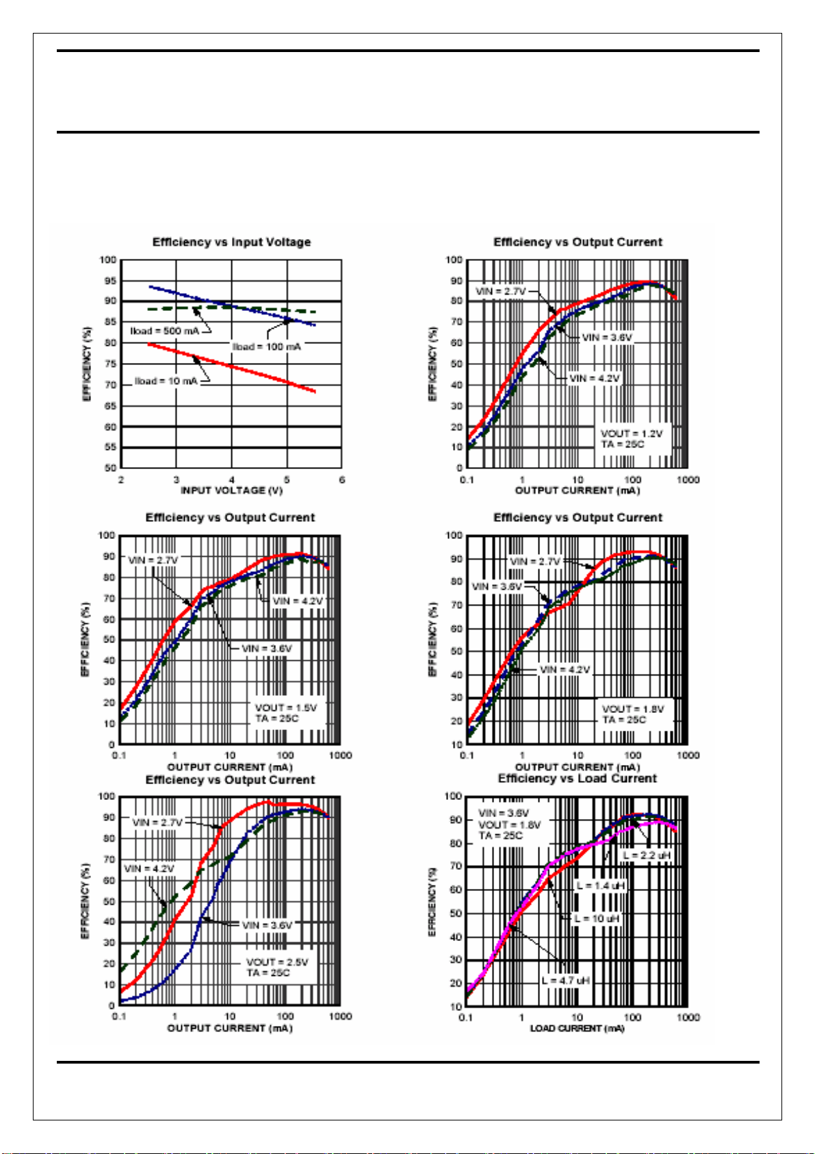
Typical Performance Characteristics
(Test Figure 1 above unless otherwise specified)
N6200
SOT-25
Lead-Free
5
May-8-2006
Page 6

NIKO-SEM
1.5 MHz, 600mA Synchronous
Step-Down Converter
N6200
SOT-25
Lead-Free
6
May-8-2006
Page 7

NIKO-SEM
1.5 MHz, 600mA Synchronous
Step-Down Converter
N6200
SOT-25
Lead-Free
Pin Description
7
May-8-2006
Page 8

NIKO-SEM
1.5 MHz, 600mA Synchronous
Step-Down Converter
PIN NAME FUNCTION
N6200
SOT-25
Lead-Free
1
2 GND Ground
3
4
5
RUN Regulator Enable control input. Drive RUN above 1.5V to turn on the part. Drive RUN below 0.3V to turn
it off. In shutdown, all functions are disabled drawing <1µA supply current. Do not leave RUN floating.
SW
IN
FB/VOU
T
Power Switch Output. It is the Switch note connection to Inductor. This pin connects to the drains of the
internal P-CH and N-CH MOSFET switches.
Supply Input Pin. Must be closely decoupled to GND, Pin 2, with a 2.2µF or greater ceramic capacitor.
VFB (N6200): Feedback Input Pin. Connect FB to the center point of the external resistor divider. The
feedback threshold voltage is 0.6V.
VOUT (N6200-1.2/N6200-1.5/N6200-1.8): Output Voltage Feedback Pin. An internal resistive divider
divides the output voltage down for comparison to the internal reference voltage.
Functional Block Diagram
Figure 2 N6200 Block Diagram
8
May-8-2006
Page 9

NIKO-SEM
1.5 MHz, 600mA Synchronous
Step-Down Converter
N6200
SOT-25
Lead-Free
Operation
N6200 is a monolithic switching mode Step-Down DC-DC converter. It utilizes internal MOSFETs to
achieve high efficiency and can generate very low output voltage by using internal reference at 0.6V. It
operates at a fixed switching frequency, and uses the slope compensated current mode architecture. This
Step-Down DC-DC Converter supplies 600mA output current at VIN = 3V with input voltage range from
2.5V to 5.5V.
Current Mode PWM Control
Slope compensated current mode PWM control provides stable switching and cycle-by-cycle current limit
for excellent load and line responses and protection of the internal main switch (P-Ch MOSFET) and
synchronous rectifier (N-CH MOSFET). During normal operation, the internal PCH MOSFET is turned on
for a certain time to ramp the inductor current at each rising edge of the internal oscillator, and switched
off when the peak inductor current is above the error voltage. The current comparator, ICOMP, limits the
peak inductor current. When the main switch is off, the synchronous rectifier will be turned on
immediately and stay on until either the inductor current starts to reverse, as indicated by the current
reversal comparator, I
, or the beginning of the next clock cycle. The OVDET comparator controls
ZERO
output transient overshoots by turning the main switch off and keeping it off until the fault is no longer
present.
Idle Mode Operation
At very light loads, the N6200 automatically enters Idle Mode. In the Idle Mode, the inductor current may
reach zero or reverse on each pulse. The PWM control loop will automatically skip pulses to maintain
output regulation. The bottom MOSFET is turned off by the current reversal comparator, I
ZERO
, and the
switch voltage will ring. This is discontinuous mode operation, and is normal behavior for the switching
regulator.
Dropout Operation
When the input voltage decreases toward the value of the output voltage, the N6200 allows the main
switch to remain on for more than one switching cycle and increases the duty cycle
(Note 5)
until it reaches
100%. The output voltage then is the input voltage minus the voltage drop across the main switch and the
inductor. At low input supply voltage, the R
of the P-Channel MOSFET increases, and the efficiency
DS(ON)
of the converter decreases. Caution must be exercised to ensure the heat dissipated not to exceed the
maximum junction temperature of the IC.
Note 5: The duty cycle D of a step-down converter is defined as:
Where TON is the main switch on time, and f
is the oscillator frequency (1.5Mhz).
OSC
9
May-8-2006
Page 10

NIKO-SEM
1.5 MHz, 600mA Synchronous
Step-Down Converter
N6200
SOT-25
Lead-Free
Maximum Load Current
The N6200 will operate with input supply voltage as low as 2.5V, however, the maximum load current
decreases at lower input due to large IR drop on the main switch and synchronous rectifier. The slope
compensation signal reduces the peak inductor current as a function of the duty cycle to prevent
sub-harmonic oscillations at duty cycles greater than 50%. Conversely the current limit increases as the
duty cycle decreases.
Layout Guidance
When laying out the PC board, the following suggestions should be taken to ensure proper operation of the
N6200. These items are also illustrated graphically in Figure 3.
1. The power traces, including the GND trace, the SW trace and the VIN trace should be kept short,
direct and wide.
2. The VFB pin should be connected directly to the feedback resistor. The resistive divider R1/R2 must
be connected between the (+) plate of C3 and ground.
3. Connect the (+) plate of C1 to the VIN pin as closely as possible. This capacitor provides the AC
current to internal power MOSFET.
4. Keep the switching node, SW, away from the sensitive VFB node.
5. Keep the (-) plates of C1 and C3 as close as possible.
N6200
Figure 3. N6200 Layout Example
10
May-8-2006
Page 11

NIKO-SEM
1.5 MHz, 600mA Synchronous
Step-Down Converter
APPLICATIONS INFORMATION
Figure 4 below shows the basic application circuit with N6200 fixed output versions.
N6200
Figure 4. Basic Application Circuit with fixed output versions
Setting the Output Voltage
N6200
SOT-25
Lead-Free
Figure 1 above shows the basic application circuit with N6200 adjustable output version. The external
resistor sets the output voltage according to the following equation:
R1=316kΩ for all outputs;
R2= 316kΩ for Vout=1.2V;
R2= 474kΩ for Vout=1.5V;
R2= 634kΩ for Vout=1.8V;
R2= 1MΩ for Vout=2.5V;
Inductor Selection
For most designs, the N6200 operates with inductors of 1µH to 4.7µH. Low inductance values are
physically smaller but require faster switching, which results in some efficiency loss. The inductor value
can be derived from the following equation:
Where ∆I
is inductor Ripple Current. Large value inductors lower ripple current and small value inductors
L
result in high ripple currents. Choose inductor ripple current approximately 35% of the maximum load
current 600mA, or ∆IL = 210mA.
11
May-8-2006
Page 12

NIKO-SEM
1.5 MHz, 600mA Synchronous
Step-Down Converter
N6200
SOT-25
Lead-Free
For output voltages above 2.0V, when light-load efficiency is important, the minimum recommended
inductor is 2.2µH. For optimum voltage-positioning load transients, choose an inductor with DC series
resistance in the 50mΩ to 150mΩ range. For higher efficiency at heavy loads (above 200mA), or minimal
load regulation (but some transient overshoot), the resistance should be kept below 100mΩ. The DC
current rating of the inductor should be at least equal to the maximum load current plus half the ripple
current to prevent core saturation (600mA+105mA). Table 1 lists some typical surface mount inductors
that meet target applications for the N6200.
Part # L (µH) Max DCR (m.) Rated D.C. Current (A) Size W x L x H (mm)
Sumida
1.4
2.2
56.2
71.2
2.52
1.75
4.5x4.0x3.5
CR43
3.3
4.7
1.5
86.2
108.7
1.44
1.15
Sumida
2.2
75
1.32
4.7x4.7x2.0
CDRH4D18
3.3
110
1.04
4.7
1.5
162
120
0.84
1.29
Toko
2.2
140
1.14
3.6x3.6x1.2
D312C
3.3
180
0.98
4.7
240
0.79
Table 1 Typical Surface Mount Inductors
Input Capacitor Selection
The input capacitor reduces the surge current drawn from the input and switching noise from the device.
The input capacitor impedance at the switching frequency shall be less than input source impedance to
prevent high frequency switching current passing to the input. A low ESR input capacitor sized for
maximum RMS current must be used. Ceramic capacitors with X5R or X7R dielectrics are highly
recommended because of their low ESR and small temperature coefficients. A 4.7µF ceramic capacitor for
most applications is sufficient.
Output Capacitor Selection
The output capacitor is required to keep the output voltage ripple small and to ensure regulation loop stability. The output
capacitor must have low impedance at the switching frequency. Ceramic capacitors with X5R or X7R dielectrics are
recommended due to their low ESR and high ripple current. The output ripple V
12
is determined by:
OUT
May-8-2006
Page 13

NIKO-SEM
1.5 MHz, 600mA Synchronous
Step-Down Converter
N6200
SOT-25
Lead-Free
SOT-25 (M5) MECHANICAL DATA
mm mm
Dimension
Min. Typ. Max.
A 0.9 1.1 e 1.9
A1 0.01 0.13 H 2.5 3.1
A2 L 0.35 0.8
b 0.3 0.5
C 0.09 0.2
Dimension
Min. Typ. Max.
D 2.8 3.0
E 1.5 1.7
D
C
L
HE
e
A
13
A1A2
May-8-2006
b
Page 14

 Loading...