

Page 1
NIKO-SEM
5 Bit Programmable Synchronous
Buck Converter with Dual LDOs
GENERAL DESCRIPTION
FEATURES
N3004
The N3004 is a 5 bit TTL-compatible input,
digital-to-analog (DAC) programmable, synchronous buck converter with dual LDOs
controller designed specifically to power the
Pentium ® II as well as the next generation of
P6 family or other high performance core
logic in desktop personal computer and file
servers CPU applications.
The N3004 switching section provides programmability of output voltage from 1.3V to
2.05V in 50mV steps and 2.0V to 3.5V in 100
mV increments and the linear sections use
external N-Channel power MOSFETs to
provide fixed output voltages of 1.5V for GTL
bus and 2.5V for clock.
The N3004 monitors all the output voltages.
A signal Power-Good signal is issued when
the core is within ±15% of the DAC setting.
Additional features are built-in over-voltage,
over-current protections for the core output
and logic compatible shutdown.
z Synchronous operation with high efficiency
z TTL-compatible 5 bit DAC, output voltage
selection from 1.3V to 3.5V programmable
z Fast transient response
z Provides 2 regulated voltages, 1.5V and
2.5V for linear section
z Power-Good output voltage monitor
z Over-Voltage and Over-Current protection
z Logic level enable input
z High performance and low cost solution
APPLICATIONS
z Powering Pentium, ® II, III or Deschutes,
K6 and other advanced processor
z High power DC to DC controller with triple
output supplies
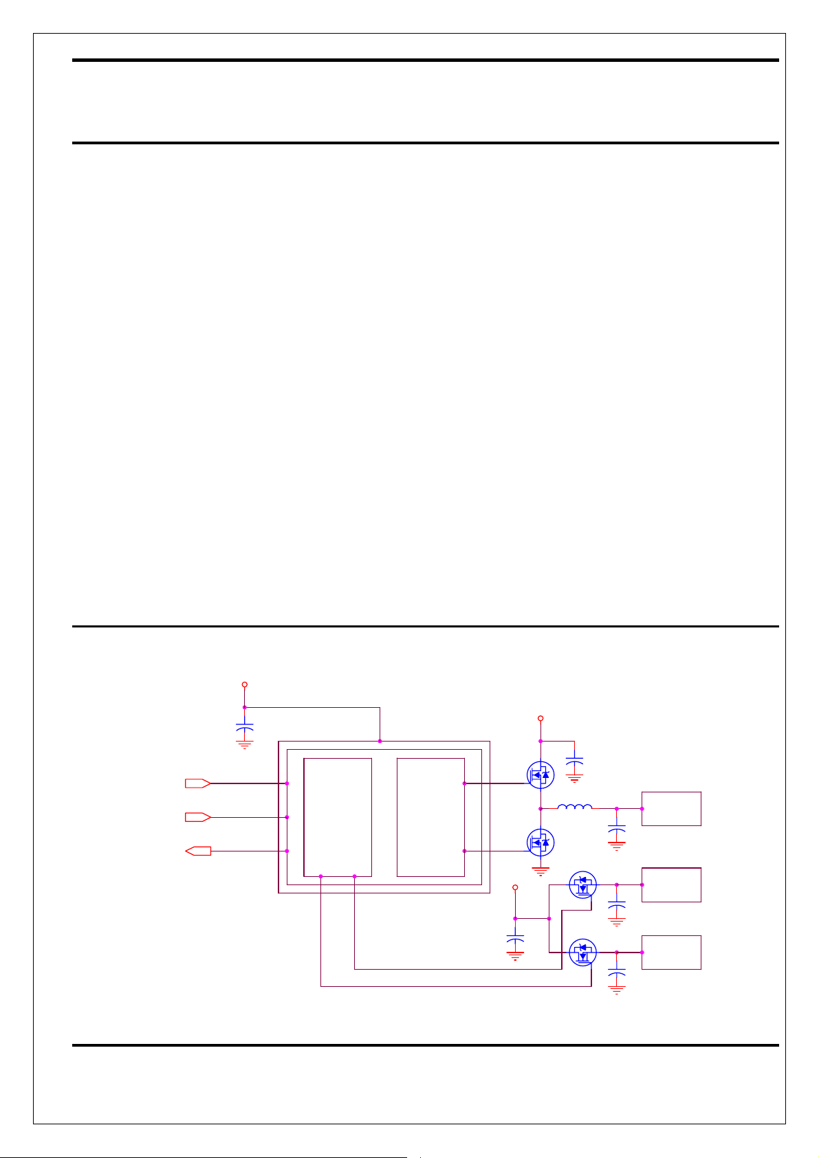
TYPICAL APPLICATION
ENABLE
VID 0~4
POWER-GOOD
12V
+
LINEAR
SECTION
SWITCHING
SECTION
3.3V
5V
+
VCORE
+
1.5V
GTC
+
+
+
BUS
2.5V
CLOCK
N3004, Motherboard Power Regulation for Computers
1
JAN-10-Y02
Page 2
NIKO-SEM
5 Bit Programmable Synchronous
N3004
Buck Converter with Dual LDOs
ABSOLUTE MAXIMUM RATINGS
PARAMETER VALUE
Supply Voltage (V5 to GND) 10V
Supply Voltage (V12 to GND) 20V
Thermal Resistance Junction to Case, θJC
Thermal Resistance Junction to Ambient, θJA
25°C/W
85°C/W
Operating Temperature Range 0 to 70°C
Storage Temperature Range -65 to +150°C
Junction Operating Temperature 0 to +125°C
Lead Temperature (Soldering, 10 Seconds) 300°C
ELECTRICAL SPECIFICATIONS
<Unless otherwise specified: V5 = 5V, V12 = 12V and TA = 25°C>
PARAMETER CONDITIONS MIN TYP MAX UNITS
SWITCHING SECTION
DAC Output Voltage (Note 1) 0.99Vs Vs 1.01Vs V
DAC Output Line Regulation 0.1 %
DAC Output Temp. Variation 0.5 %
VID Input LO 0.4 V
VID Input HI 2 V
VID Input Internal Pull-Up
Resistor to V5
27
KΩ
POWER GOOD SECTION
Power Good Threshold Voltage
85 115 %
Power Good Output LO IL = 3mA 0.4 V
Power Good Output HI
RL = 5KΩ pull up to 5V
4.8 V
SOFT START SECTION
Soft Star Current CS+ =0V, CS- =5V 10
μA
UVLO SECTION
UVLO Threshold for V12 Supply ramping up 9.2 10 10.8 V
UVLO Hysterises for V12 0.3 0.4 .05 V
UVLO Threshold for V5 Supply ramping up 4.1 4.3 4.5 V
UVLO Hysterises for V5 0.2 0.3 0.4 V
ERROR COMPARATOR SECTION
Input Bias Current 2
μA
Input Offset Voltage -2 +2 mV
Delay to Output V
= 10mV 100 nS
DIFF
2
JAN-10-Y02
Page 3
NIKO-SEM
5 Bit Programmable Synchronous
N3004
Buck Converter with Dual LDOs
PARAMETER CONDITIONS MIN TYP MAX UNITS
CURRENT LIMIT SECTION
C.S Threshold Set Current 160 200 240
μA
C.S Comparator Offset Voltage -5 +5 mV
Hiccup Duty Cycle
Css = 0.1μF
2 %
SUPPLY CURRENT
Operating Supply Current CL=3000 pF
V5 20
V12 14 mA
OUTPUT DRIVERS SECTION
Rise Time CL = 3,000pF 60 100 nS
Fall Time CL = 3,000pF 60 130 nS
Dead Band Time CL = 3,000pF 100 200 300 nS
OSCILLATOR SECTION
Oscillator Frequency CL = 150pF 220 KHz
Oscillator Valley 0.2 V
Oscillator Peak V5 V
LINEAR SECTIONS
V
& V
FB1
Input Bias Current 2
I
DRIVER1
Note 1: Vs refers to the set point voltage given in Table 1.
1.40 1.50 1.60 V
FB2
or I
DRIVER2
50 mA
μA
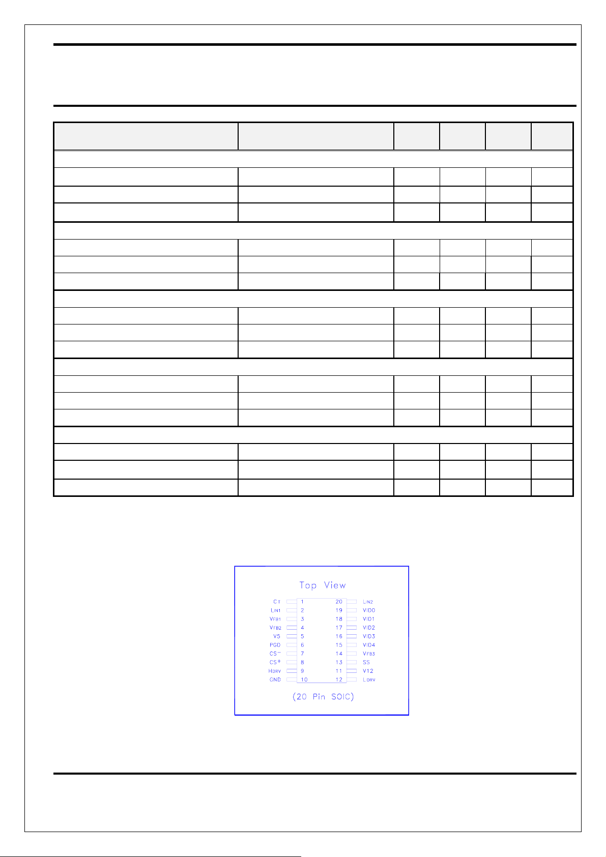
PIN CONFIGURATIONS
3
JAN-10-Y02
Page 4

NIKO-SEM
5 Bit Programmable Synchronous
Buck Converter with Dual LDOs
PIN DEFINITIONS
Pin # Pin Name Pin Function Description
N3004
1 CT
2 L
3 V
4 V
IN1
FB1
FB2
The oscillator frequency is programmed by connecting an external capacitor from this pin to GND. Operation in range of 50 KHz to 500 KHz.
Gate drive output regulator, Linear 1 for GTL+ or Clock supply.
Feedback input for L
Feedback input for L
IN1
IN2
.
.
5 V5 5V supply voltage.
6 PGD* Open collector logic output, high if VO within 10% of set point.
7 CS-
8
CS+
Current sense input (Negative), connected to the Source of the power
MOSFET for the core supply.
Current sense input (Positive), connected to the Drain of the power MOSFET for the core supply. An external resistor programs the C.S threshold
depending on the R
of the power MOSFET. An external capacitor is
DS(ON)
placed in parallel with the programming resistor to provide high frequency
noise filtering.
9 H
10
High side driver output.
DRV
GND
This pin serves as the ground pin and must be connected directly to the
ground plane. A high frequency capacitor (0.1 to 1μF) must be connected
directly from V5 and V12 pins to this pin for noise free operation.
11 L
12
Low side driver output.
DRV
V12
12V supply voltage for LINEAR section. A high frequency capacitor (0.1 to
1μF) must be connected directly from this pin to GND pin in order to
supply the peak current to the power MOSFET during the transients.
13
SS
This pin provides the soft start for the switching regulator. An internal
current source charges an external capacitor that is connected from this
pin to the GND which ramps up the outputs of the switching regulator,
preventing the outputs from overshooting as well as limiting the input
current. The second function of the soft start cap is to provide long off time
(HICCUP) for the synchronous MOSFET during current limiting.
14 V
Feedback input for V
FB3
CORE
.
15 VID4* Programming input (MSB).
16 VID3* Programming input.
17 VID2* Programming input.
18 VID1* Programming input.
19 VID0* Programming input (LSB).
20 L
* : All logic level inputs and outputs are open collector TTL compatible.
Gate drive output regulator, Linear 2 for GTL+ or Clock supply.
IN2
4
JAN-10-Y02
Page 5

NIKO-SEM
5 Bit Programmable Synchronous
Buck Converter with Dual LDOs
OUTPUT SET POINT VOLTAGE vs VID CODES
− Table 1 −
Vs VID4 VID3 VID2 VID1 VID0
1.30 0 1 1 1 1
1.35 0 1 1 1 0
1.40 0 1 1 0 1
1.45 0 1 1 0 0
1.50 0 1 0 1 1
1.55 0 1 0 1 0
1.60 0 1 0 0 1
1.65 0 1 0 0 0
1.70 0 0 1 1 1
1.75 0 0 1 1 0
1.80 0 0 1 0 1
1.85 0 0 1 0 0
1.90 0 0 0 1 1
1.95 0 0 0 1 0
2.00 0 0 0 0 1
2.05 0 0 0 0 0
2.00 1 1 1 1 1
2.10 1 1 1 1 0
2.20 1 1 1 0 1
2.30 1 1 1 0 0
2.40 1 1 0 1 1
2.50 1 1 0 1 0
2.60 1 1 0 0 1
2.70 1 1 0 0 0
2.80 1 0 1 1 1
2.90 1 0 1 1 0
3.00 1 0 1 0 1
3.10 1 0 1 0 0
3.20 1 0 0 1 1
3.30 1 0 0 1 0
3.40 1 0 0 0 1
3.50 1 0 0 0 0
N3004
5
JAN-10-Y02
Page 6

NIKO-SEM
5 Bit Programmable Synchronous
Buck Converter with Dual LDOs
APPLICATION CIRCUIT
N3004
5V
VID 0
VID 1
VID 2
VID 3
VID 4
12V
P.G
1000uF
+
3.3V
1uF
10K
1uF
+
0.1uF
1uF
+
150pF
0.1uF
2 uH
VCC
VID 0
VID 1
VID 2
VID 3
VID 4
V12
SS
CT
PGD
N3004
1000uF x 2
CS+
HDRV
CS-
LDRV
VFB3
LIN1
LIN2
VFB2
VFB1
GND
+
2.21K
MOSFET
P50N02L x 2
10
220pF
1K
470pF
10
Short or
5 OHM
1K
10K
150
100
2.5uH
SBD
1A/30V
100
100
100
1500uF x 5
3.3V
+
680uF
0.01uF
++ ++ + +
P3055LD x 2
0.1uF
+
10K
MOSFET
0.01uF
100
VCORE
1.5V
GTC
BUS
+
680uF
2.5V
CLOCK
+
220uF
6
JAN-10-Y02
Page 7

NIKO-SEM
Dimension
A 12.6 13.0 H 0.4 1.27
B 7.3 7.7 I 0.23 0.32
C 10 10.65 J 0.25 0.74
D 0.33 0.51 K
E 1.27 L
F 2.1 2.3 2.5 M
G 0.1 0.3 N
5 Bit Programmable Synchronous
Buck Converter with Dual LDOs
SOIC-20 (DW) MECHANICAL DATA
mm mm
Dimension
Min. Typ. Max.
N3004
Min. Typ. Max.
0°
8°
7
JAN-10-Y02
 Loading...