

Page 1
Date:- 20 Nov, 2001
WESTCODE
Phase Control Thyristor
Types N2500VC120 to N2500VC160
Absolute Maximum Ratings
VOLTAGE RATINGS
V
DRM
V
DSM
V
RRM
V
RSM
I
T(AV)
I
T(AV)
I
T(AV)
I
T(RMS)
I
T(d.c.)
I
TSM
I
TSM2
I2tI
I2t
diT/dt
V
RGM
P
G(AV)
P
GM
V
GD
T
HS
T
stg
Repetitive peak off-state voltage, (note 1) 1200-1600 V
Non-repetitive peak off-state voltage, (note 1) 1200-1600 V
Repetitive peak reverse voltage, (note 1) 1200-1600 V
Non-repetitive peak reverse voltage, (note 1) 1300-1700 V
OTHER RATINGS
Mean on-state current. T
Mean on-state current. T
Mean on-state current. T
Nominal RMS on-state current. T
D.C. on-state current. T
Peak non-repetitive surge tp=10ms, Vrm=0.6V
Peak non-repetitive surge tp=10ms, V
2
t capacity for fusing tp=10ms, Vrm=0.6V
I2t capacity for fusing tp=10ms, V
Maximum rate of rise of on-state current (repetitive), (Note 6) 150 A/µs
Maximum rate of rise of on-state current (non-repetitive), (Note 6) 300 A/µs
Peak reverse gate voltage 5 V
Mean forward gate power 5 W
Peak forward gate power 30 W
Non-trigger gate voltage, (Note 7) 0.25 V
Operating temperature range -40 to +125 °C
Storage temperature range -40 to +150 °C
=55°C, (note 2) 2500 A
sink
=85°C, (note 2) 1684 A
sink
=85°C, (note 3) 992 A
sink
=25°C, (note 2) 4985 A
sink
=25°C, (note 4) 4199 A
sink
, (note 5) 37000 A
RRM
≤
10V, (note 5)
rm
, (note 5) 6.85×10
RRM
≤
10V, (note 5)
rm
Data Sheet Issue:- 1
MAXIMUM
LIMITS
MAXIMUM
LIMITS
45000 A
6
10.1×10
6
UNITS
UNITS
A2s
A2s
Notes: -
1)
De-rating factor of 0.13% per °C is applicable for Tj below 25°C.
2)
Double side cooled, single phase; 50Hz, 180° half-sinewave.
3)
Single side cooled, single phase; 50Hz, 180° half-sinewave.
4)
Double side cooled.
5)
Half-sinewave, 125°C Tj initial.
6)
VD=67% V
7)
Rated V
Data Sheet. Types N2500VC120 to N2500VC160 Issue 1. Page 1 of 10 November, 2001
, ITM=1000A, IFG=2A, t
DRM
.
DRM
≤
0.5µs, T
r
case
=125°C.
Page 2
WESTCODE
Positive development in power electronics
Characteristics
N2500VC120 to N2500VC160
PARAMETER MIN. TYP. MAX. TEST CONDITIONS
V
V
r
S
dv/dt Critical rate of rise of off-state voltage 200 - - VD=80% V
I
DRM
I
RRM
V
I
GT
I
H
t
gd
t
gt
Q
Q
I
rm
t
rr
t
q
R
Maximum peak on-state voltage - - 1.28 ITM=3220A V
TM
Threshold voltage - - 0.88 V
0
Slope resistance - - 0.124
Peak off-state current - - 150 Rated V
Peak reverse current - - 150 Rated V
Gate trigger voltage - - 3.0 V
GT
T
Gate trigger current - - 300
DRM
RRM
=25°C, VD=10V, IT=3A
j
Holding current - - 1000 Tj=25°C mA
Gate controlled turn-on delay time - 1.0 2.0
Turn-on time - 1.5 2.5
Recovered Charge - 2200 - µC
rr
Recovered Charge, 50% chord - 1300 1800 µC
ra
Reverse recovery current - 100 - A
=67%V
V
D
I
=2A, tr=0.5µs, Tj=25°C
FG
I
=1000A, tp=1000µs, di/dt=10A/µs,
TM
V
=50V
r
Reverse recovery time, 50% chord - 20.0 -
ITM=1000A, tp=1000µs, di/dt=10A/µs,
V
=50V, Vdr=33%V
r
ITM=1000A, tp=1000µs, di/dt=10A/µs,
V
=50V, Vdr=33%V
r
Turn-off time
Thermal resistance, junction to heatsink
th(j-hs)
- 500 800
- 800 1200
--0.017 Double side cooled K/W
--
0.034 Single side cooled K/W
(Note 1)
, linear ramp, Gate O/C
DRM
, ITM=2000A, di/dt=10A/µs,
DRM
, dVdr/dt=20V/µs
DRM
, dVdr/dt=200V/µs
DRM
UNITS
m
V/µs
mA
mA
mA
µs
µs
µs
F Mounting force 27 - 34 kN
W
Weight - 1.0 - kg
t
Ω
Notes: -
Unless otherwise indicated Tj=125°C.
1)
Data Sheet. Types N2500VC120 to N2500VC160 Issue 1. Page 2 of 10 November, 2001
Page 3
WESTCODE
Notes on Ratings and Characteristics
1.0 Voltage Grade Table
Positive development in power electronics
N2500VC120 to N2500VC160
V
Voltage Grade
12 1200 1300 810
14 1400 1500 930
16 1600 1700 1040
2.0 Extension of Voltage Grades This report is applicable to other and higher voltage grades when supply has been agreed by Sales/Production.
3.0 De-rating Factor A blocking voltage de-rating factor of 0.13%/°C is applicable to this device for Tj below 25°C.
4.0 Repetitive dv/dt Standard dv/dt is 1000V/µs.
5.0 Rate of rise of on-state current The maxim um un-primed rate of r ise of on-state current mus t not ex c eed 300A/µs at any time during turnon on a non-repetitive basis. For repetitive performance, the on-state rate of rise of current must not exceed 150A/µs at any time during turn-on. Note that these values of rate of rise of current apply to the total device current including that from any local snubber network.
6.0 Gate Drive The recomm ended pulse gate drive is 30V, 15Ω with a short-circuit current rise time of not more than
0.5µs. This gate drive must be applied when using the full di/dt capability of the device.
DRM VDSM VRRM
V
V
RSM
V
V
V
D
DC V
R
The pulse duration may need to be configured acc ording to the application but should be no shorter than
20µs, otherwise an increase in pulse current may be needed to supply the necessary charge to trigger.
7.0 Computer Modelling Parameters
7.1 Device Dissipation Calculations
∆
2
4
=
I
AV
00
2
Where V0=0.88V, rs=0.124m
R
= Supplementary thermal impedance, see table below.
th
ff
= Form factor, see table below.
Conduction Angle 30° 60° 90° 120° 180° 270° d.c.
Square wave Double Side Cooled 0.0263 0.0237 0.022 0.0207 0.0192 0.0179 0.0171
Square wave Single Side Cooled 0.0438 0.0418 0.040 0.038 0.0367 0.0357 0.034
Sine wave Double Side Cooled 0.0238 0.021 0.0196 0.0187 0.0169
Sine wave Single Side Cooled 0.0426 0.0396 0.0382 0.0373 0.0356
Ω,
2
2
⋅⋅
rff
s
Supplementary Thermal Impedance
⋅⋅⋅++−
WrffVV
AVs
and:
W
AV
=
R
max
T
th
−=∆
TTT
Hsj
Form Factors
Conduction Angle 30° 60° 90° 120° 180° 270° d.c.
Square wave 3.46 2.45 2 1.73 1.41 1.15 1
Sine wave 3.98 2.78 2.22 1.88 1.57
Data Sheet. Types N2500VC120 to N2500VC160 Issue 1. Page 3 of 10 November, 2001
Page 4

WESTCODE
=
=
p
=
p
=
7.2 Calculating VT using ABCD Coefficients The on-state characteristic I (i) the well established V (ii) a set of constants A, B, C, D, forming the coefficients of the representative equation for V
Positive development in power electronics
terms of I
given below:
T
vs. VT, on page 5 is represented in two ways;
T
and rs tangent used for rating purposes and
0
N2500VC120 to N2500VC160
T
in
()
ln
The constants, derived by curve fitting soft ware, are given below for both hot and c old c harac teris tic s. T he
resulting values for V
that plotted.
7.3 D.C. Thermal Impedance Calculation
Where p = 1 to n, n is the number of terms in the series and:
Duration of heating pulse in seconds.
t
r
Thermal resistance at time t.
t
Amplitude of pth term.
r
τ
Time Constant of rth term.
agree with the true device characteristic over a current range, which is limited to
T
125°C Coefficients
A 0.592114202
B -7.608075×10
C 6.807×10
D 9.342666×10
=
np
∑
=
p
1
1
pt
-3
-5
-3
−
t
τ
p
−⋅=
err
⋅+⋅+⋅+=
IDICIBAV
TTTT
D.C. Double Side Cooled
Term1234
r
p
τ
p
Term1234567
r
p
τ
p
8.0 Reverse recovery ratings (i) Qra is based on 50% Irm chord as shown in Fig. 1.
(ii) Q
rr
(iii)
0.0204 4.47×10
9.877 5.385 0.781 0.161 0.0524 0.0106 1.77×10
is based on a 150µs integration time.
i.e.
8.74×10
-3
1.328 0.157 0.0242 2.3×10
D.C. Single Side Cooled
-3
150
=
FactorK
∫
0
µ
s
rrrr
2.66×10
dtiQ
.
=
t
1
t
5.08×10
-3
2
-3
4.62×10
-3
-3
1.08×10
Fig. 1
1.54×10
-3
1.80×10
-3
1.50×10
-3
-3
1.29×10
-3
-3
Data Sheet. Types N2500VC120 to N2500VC160 Issue 1. Page 4 of 10 November, 2001
Page 5

WESTCODE
Positive development in power electronics
N2500VC120 to N2500VC160
Curves
Figure 1 - On-state characteristics of Limit device Figure 2 - Transient Thermal Impedance
0.1
N2500VC120-160
0.01
Issue 1
(A)
TM
10000
Tj = 25°C
Tj = 125°C
SSC
0.034K/W
DSC
0.017K/W
1000
Instantaneous On-state current - I
N2500VC120-160
Issue 1
100
00.511.52
Instantaneous On-state voltage - V
(V)
TM
0.001
Transient thermal impedance (K/W)
0.0001
0.00001
1E-05 0.0001 0.001 0.01 0.1 1 10 100
Time (s)
Figure 3 - Gate Characteristics - Trigger Limits Figure 4 - Gate Characteristics - Power Curves
7
N2500VC120-160
Issue 1
Tj=25°C
6
5
Max VG dc
25
N2500VC120-160
Tj=25°C
20
Issue 1
Max VG dc
15
(V)
4
G
IGT, V
3
Gate Voltage - V
GT
(V)
G
10
Gate Voltage - V
PG Max 30W dc
2
-10°C
125°C
25°C
-40°C
Min VG dc
5
PG 5W dc
1
IGD, V
GD
0
0 0.2 0.4 0.6 0.8
Gate Current - I
Data Sheet. Types N2500VC120 to N2500VC160 Issue 1. Page 5 of 10 November, 2001
(A)
G
0
0246810
Gate Current - I
Min VG dc
(A)
G
Page 6

WESTCODE
Positive development in power electronics
N2500VC120 to N2500VC160
Figure 5 – Recovered Charge, Q
10000
(µC)
rr
Recovered charge - Q
1000
1 10 100 1000
di/dt (A/µs)
rr
4000A
2000A
1000A
500A
N2500VC120-160
Tj=125°C
Issue 1
Figure 6 – Recovered charge, Qra (50% chord)
10000
, 50% chord (µC)
ra
Recovered charge - Q
1000
1 10 100 1000
di/dt (A/µs)
N2500VC120-160
Issue 1
Tj=125°C
4000A
2000A
1000A
500A
Figure 7 – Reverse recovery current, I
1000.00
(A)
rm
Reverse recovery current - I
N2500VC120-160
Issue 1
Tj=125°C
100.00
10.00
1 10 100 1000
di/dt (A/µs)
rm
4000A
2000A
1000A
500A
Figure 8 – Reverse recovery time, trr (50% chord)
100
(µs)
rr
10
Reverse recovery time (50% chord) - t
1
1 10 100 1000
di/dt (A/µs)
N2500VC120-160
Issue 1
Tj=125°C
4000A
2000A
1000A
500A
Data Sheet. Types N2500VC120 to N2500VC160 Issue 1. Page 6 of 10 November, 2001
Page 7

WESTCODE
Positive development in power electronics
N2500VC120 to N2500VC160
Figure 9 – On-state current vs. Power dissipation – Double Side Cooled (Sine wave)
7000
6000
5000
30°
4000
3000
Maximum forward dissipation (W)
2000
1000
0
0 1000 2000 3000 4000
Mean forward current (A) (Whole cycle averaged)
90°
60°
180°
120°
N2500VC120-160
Issue 1
Figure 10 – On-state current vs. Heatsink temperature - Double Side Cooled (Sine wave)
150
125
100
75
50
Maximum permissable heatsink temperature (°C)
25
0
0 500 1000 1500 2000 2500 3000 3500
Mean forward current (A) (Whole cycle averaged)
30° 60° 90° 120° 180°
N2500VC120-160
Issue 1
Figure 11 – On-state current vs. Power dissipation – Double Side Cooled (Square wave)
7000
6000
5000
4000
d.c.
3000
Maximum forward dissipation (W)
2000
1000
0
0 1000 2000 3000 4000 5000
Mean Forward Current (Amps) (Whole Cycl e Averaged)
270°
180°
120°
90°
60°
30°
N2500VC120-160
Issue 1
Figure 12 – On-state current vs. Heatsink temperature - Double Side Cooled (Square wave)
150
125
100
75
50
Maximum permissible heatsink temperature (°C)
25
0
0 1000 2000 3000 4000 5000
Mean Forward Current (Amps) (Whol e C ycle Av er aged)
N2500VC120-160
Issue 1
30°
60°
90°
120°
180°
270°
d.c.
Data Sheet. Types N2500VC120 to N2500VC160 Issue 1. Page 7 of 10 November, 2001
Page 8

WESTCODE
Positive development in power electronics
N2500VC120 to N2500VC160
Figure 13 – On-state current vs. Power dissipation – Single Side Cooled (Sine wave)
3000
180°
120°
90°
2500
2000
1500
1000
Maximum forward dissipation (W)
500
0
0 500 1000 1500 2000
Mean forward current (A) (Whole cycle averaged)
30°
60°
N2500VC120-160
Issue 1
Figure 14 – On-state current vs. Heatsink temperature - Single Side Cooled (Sine wave)
150
125
100
75
50
Maximum permissable heatsink temperature (°C)
25
0
0 500 1000 1500 2000 2500
Mean forward current (A) (Whole cycle averaged)
30° 60° 90° 120°
N2500VC120-160
Issue 1
180°
Figure 15 – On-state current vs. Power dissipation – Single Side Cooled (Square wave)
3000
2500
2000
d.c.
270°
180°
1500
1000
Maximum forward dissipation (W)
500
0
0 500 1000 1500 2000 2500
Mean Forward Current (Amps) (Whole Cycl e Averaged)
120°
90°
60°
30°
N2500VC120-160
Issue 1
Figure 16 – On-state current vs. Heatsink temperature - Single Side Cooled (Square wave)
150
125
100
75
50
Maximum permissible heatsink temperature (°C)
25
0
0 500 1000 1500 2000 2500
Mean Forward Current (Amps) (Whole Cycl e Averaged)
N2500VC120-160
Issue 1
30°
60°
90°
120°
180°
270°
d.c.
Data Sheet. Types N2500VC120 to N2500VC160 Issue 1. Page 8 of 10 November, 2001
Page 9

WESTCODE
Positive development in power electronics
Figure 17 – Maximum surge and I2t Ratings
N2500VC120 to N2500VC160
1000000
N2500VC120-160
Issue 1
Tj (initial) = 125°C
100000
Total peak half sine surge current (A)
10000
135101 5 10 50 100
I
TSM
I2t: V
: 60% V
RRM
RRM
≤
10V
I2t: 60% V
I
: V
TSM
RRM
RRM
≤
10V
1.00E+08
1.00E+07
1.00E+06
s)
2
t (A
2
Maximum I
Duration of surge (ms) Duration of surge (cycles @ 50Hz)
Data Sheet. Types N2500VC120 to N2500VC160 Issue 1. Page 9 of 10 November, 2001
Page 10
WESTCODE
Positive development in power electronics
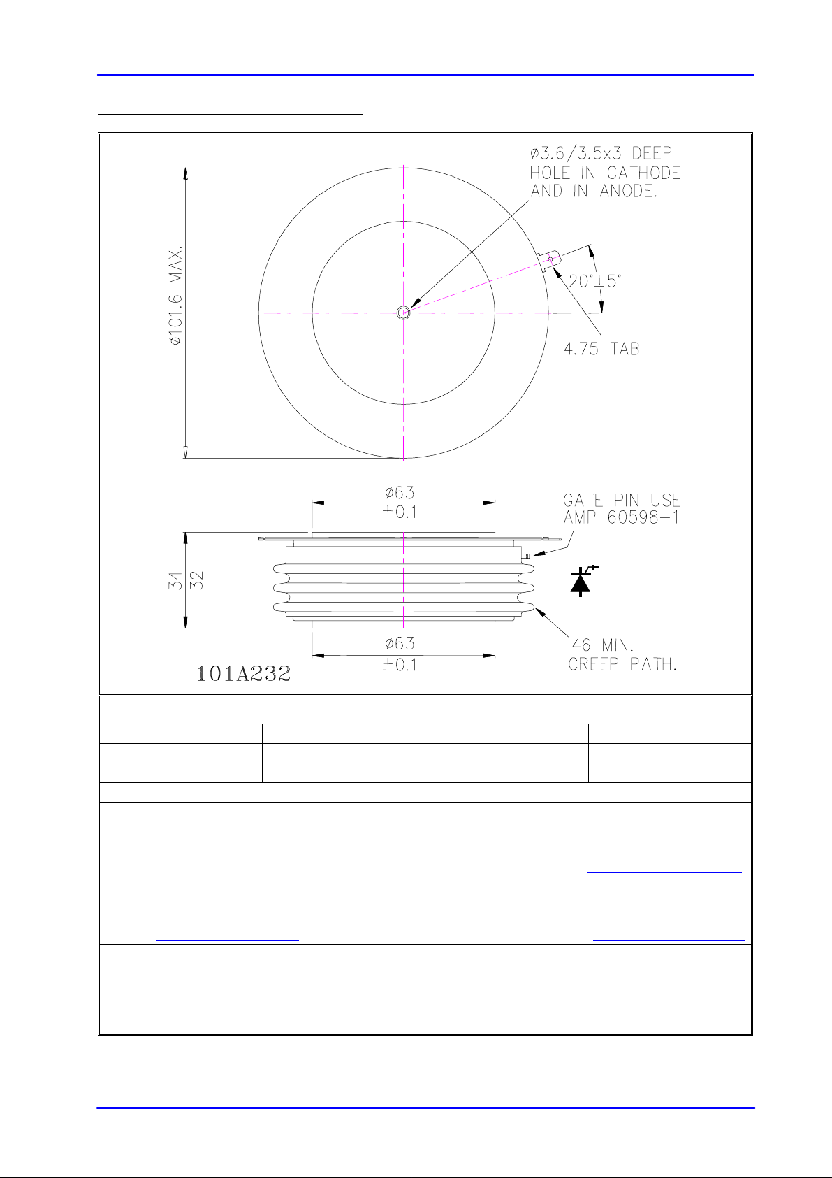
Outline Drawing & Ordering Information
N2500VC120 to N2500VC160
ORDERING INFORMATION
N2500 VC
Fixed
Type Code
Typical order code: N2500VC120 – 1200V V
Fixed
Outline Code
DRM/VRRM
, 34mm clamp height capsule.
WESTCODE
Internet: http://www.westcode.com
The information contained herein is confidential and is protected by Copyright. The information may not be used or disclosed
except with the written permission of and in the manner permitted by the proprietors Westcode Semiconductors Ltd.
In the interest of product improvement, Westcode reserves the right to change specifications at any time without prior notice.
Devices with a suffix code (2-letter or letter/digit/letter combination) added to their generic code are not necessarily subject to
the conditions and limits contained in this report.
Data Sheet. Types N2500VC120 to N2500VC160 Issue 1. Page 10 of 10 November, 2001
(Please quote 10 digit code as bel ow)
♦ ♦
♦ ♦
♦ ♦♦ ♦
Voltage Code
12-16
UK: Westcode Semiconductors Ltd.
P.O. Box 57, Chippenham, Wiltshire, England. SN15 1JL.
Tel: +44 (0) 1249 444524 Fax: +44 (0) 1249 659448
E-Mail: WSL.sales@westcode.com
USA: Westcode Semiconductors Inc.
3270 Cherry Avenue, Long Beach, California 90807
Tel: +1 (562) 595 6971 Fax: +1 (562) 595 8182
E-Mail: WSI.sales@westcode.com
© Westcode Semiconductors Ltd.
0
Fixed turn-off
time code
 Loading...