

Page 1
The MXD205 is a very low cost dual-axis acceleration sensor on a monolithic IC. With no moving parts,
the device is extremely reliable and is manufactured on a submicron CMOS process enabling small
geometries and small die size, resulting in low overall cost and high functionality. The MXD205 is primarily designed for applications requiring high performance and where overall system cost is a driving
factor in component selection. The MXD205 measures acceleration with a full-scale range of up to ±5
g
and produces a PWM digital signal output. Sensor is shipped with a duty cycle period of 10 milliSeconds (100 Hz). Special order sensors are available with a duty cycle period of 2.5 milli-Seconds
(400 Hz). Typical noise floor is .004 % Duty Cycle/√Hz, allowing signals below 1.0 milli-
g to be resolved.
Frequency response extends to 40 Hz. The frequency response can be extended to 160 Hz with the
implementation of a simple external circuit..
The MXD205 is a dc accelerometer with the capability to measure both ac acceleration, (typ-
ical of vibration) or dc accelerations, (such as inertial force or constant, gravity-induced accelerations).
The MXD205 offers digital output signals which duty cycles (ratio of pulse width to period)
are proportional to the acceleration in each of the axes of sensitivity. The outputs can be measured
directly with a microprocessor counter, eliminating the need for A/D converter or glue logic. The output
duty cycle is programmable over a wide range of sensitivity. MXD205 offers a calibrated temperature
sensor output with a positive temperature coefficient of 5.0 mV/°C. This device can be temperature
compensated easily. The change in sensitivity over the temperature range –40°C to 125°C is predictable and follows the physical gas laws. The following equation can be used to predict the sensitivi-
ty at any given temperature:
SINX (TIN)
2.67
= S
FIN
X (T
FIN
)
2.67
(Temperature in °K) See Application Note
(AN-00MX-001).
The MXD205 is available in a metal can (TO-100) or a surface mount (LCC); both are hermetic and are specified over the temperature range -40°C to 125°C.
General Description
MXD205 (DIGITAL)
Features
Low Cost, 5.0g, Dual Axis Accelerometer
with Digital Outputs
Applications
• Automotive - Vehicle Security/Active Suspension/ABS/HED Angle Control
• Security - Gas Line/Elevator/Fatigue Sensing
• Office Automation Equipment - Computer Peripherals/Disk Drives/PDA’s/Mouse
Smart Pens/Cell Phones/Printer Head Acceleration Sensor
• Gaming - Joystick/RF Interface/Menu Selection
• White Goods - Spin Control/Cooktop Vibration
Information furnished by MEMSIC is believed to be
accurate and reliable. However, no responsibility is
assumed by MEMSIC for its use, nor for any infringements of patents or other rights of third parties which
may result from its use. No license is granted by
implications or otherwise under any patent or patent
rights of MEMSIC.
Technical information.
Subject to change without notice.
®MEMSIC, Inc. 2000.
100 Burtt Road, Andover, MA 01810
Tel: 978.623.8188 • Fax: 978.623.9945
www.memsic.com
MXD205 DIGITAL Data Sheet J 8/1/01
Page 1 of 8
Data Sheet
MXD205
• Dual axis acceleration outputs
• Digital outputs
• 1.0 mg Resolution in 1Hz bandwidth
• 40 Hz Bandwidth expandable to 160 Hz
• Quiescent Supply Voltage: 3.5 mA
• 0g output 50% duty cycle
• 50,000g shock survival
• 2.70V to 5.25V Single Supply
• On-chip mixed signal processing
• Continuous sensors self test
• Temperature sensor output (Tout) 5mV/°K
• Packaged in 8 pin LCC SMD or
10 pin TO-100 THRU-HOLE
• Hermetically sealed packaging
• Reference voltage (V
REF
) 2.50V
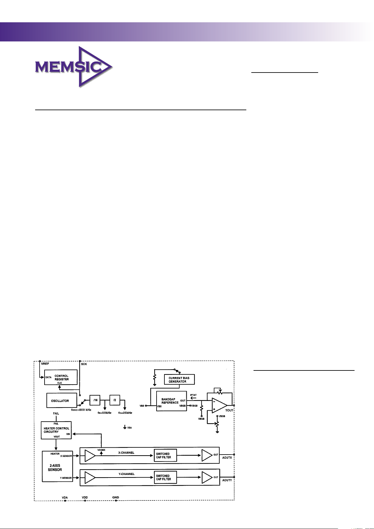
Block Diagram of MX20XX
Page 2
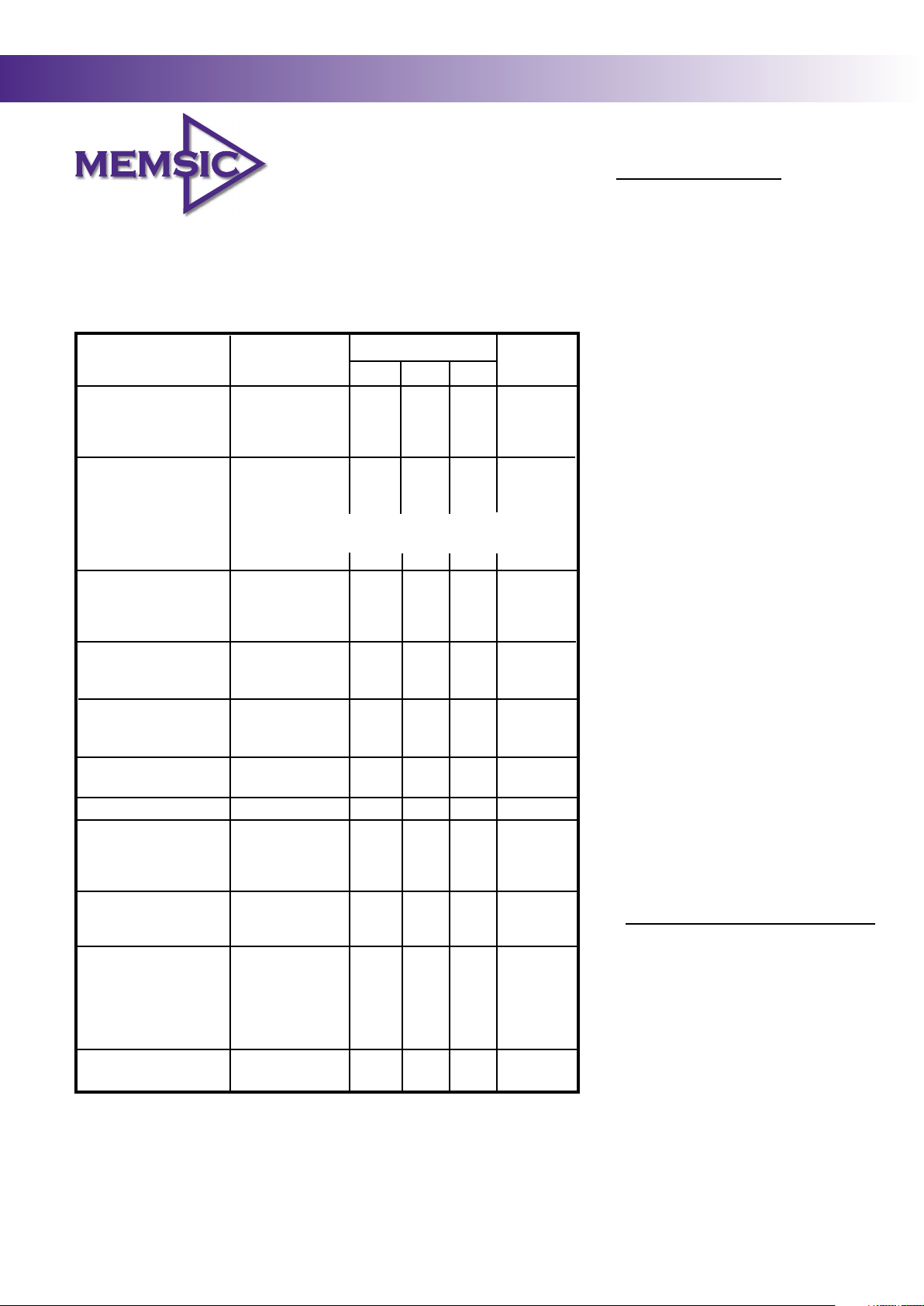
MXD205 SPECIFICATIONS
Digital Electrical Characteristics
NOTES
1
Guarantee by measurements of initial offset
and sensitivity.
2
Alignment error is specified as the angle between
the true and indicated axis of sensitivity.
3
Cross-axis sensitivity is the algebraic sum of the
alignment and the inherent sensitivity errors.
4
Specification refers to the maximum change in
parameter from its initial value at 25°C to its
worst case value at Tmin to Tmax of the specified
temperature range.
5
Noise density (% Duty Cycle√/Hz) is the average
noise at any frequency in the bandwidth of the device.
6
The voltage is required to ramp full scale before
making a measurement.
7
Note: Frequency compensating circuit will achieve
160 Hz operations.
8
Defined as the output change from ambient to
maximum temperature or minimum. Output change
expressed in % change of duty cycle.
9
For more details refer to
Application Note (AN-00MX-001).
All min and max specifications are subject to change
without notification.
Information furnished by MEMSIC is believed to be
accurate and reliable. However, no responsibility is
assumed by MEMSIC for its use, nor for any infringements of patents or other rights of third parties which
may result from its use. No license is granted by
implications or otherwise under any patent or patent
rights of MEMSIC.
Technical information.
Subject to change without notice.
Page 2 of 8
Data Sheet
®MEMSIC, Inc. 2000.
100 Burtt Road, Andover, MA 01810
Tel: 978.623.8188 • Fax: 978.623.9945
www.memsic.com
MXD205 DIGITAL Data Sheet J 8/1/01
MXD205
Temperature Changes
8
Delta from 25°C per formula
S
IN
X (TIN)
2.67
= S
FIN
X (T
FIN
)
2.67
SENSOR Each axis
Measurement Range
1
Nonlinearity Best Fit Straight
Alignment Error
2
Line
SENSITIVITY Each axis
Output in Duty Cycle per g
ZERO g BIAS LEVEL Each axis 48 50 52 % Duty Cycle
0g Offset vs. 2.0 mg/°C
Temperature
4
NOISE PERFORMANCE
Noise Density
5
@ +25°C .004 .005 % Duty Cycle
% Duty Cycle /√Hz
FREQUENCY RESPONSE
3 dB Bandwidth 40 Hz
3 dB Bandwidth
7
160 Hz
SELF TEST
Voltage Delta at outputs Continuous,
@5V Supply Output rails with 5.0 V
@2.7V Supply failure 2.7 V
X, Y OUTPUTS Digital signal of100Hz
Rise/Fall Time 90 100 110 nsec
TEMPERATURE RANGE
Operating Range
Tout Voltage 25°C 1.23 1.25 1.27 V
Temp sensor sensitivity 5 mV/°K
V REFERENCE
9
25°C 2.4 2.5 2.6 V
+/- 5.0
2
+/- 1.0 +/- 2.5
4.0
% Duty Cycle
/g
g
% of FS
degrees
Min Typ Max
Parameter Conditions
MEMSIC MXD205 Units
2.7 5.25 V
3.0 3.5 mA
4.0 4.5 mA
200 400 ms
-40 125 °C
POWER SUPPLY
Operating Voltage Range
Specified Performance
Quiescent Supply Current @ 5V
Quiescent Supply Current @ 2.7V
Turn-On Time
6
Measurements @ 25°C Acceleration = 0g unless otherwise noted
V
DD, VDA = 5.0V unless otherwise specified
Cross-Axis Sensitivity
3
X sensor to Y sensor +/- 2 %
Page 3
Data Sheet
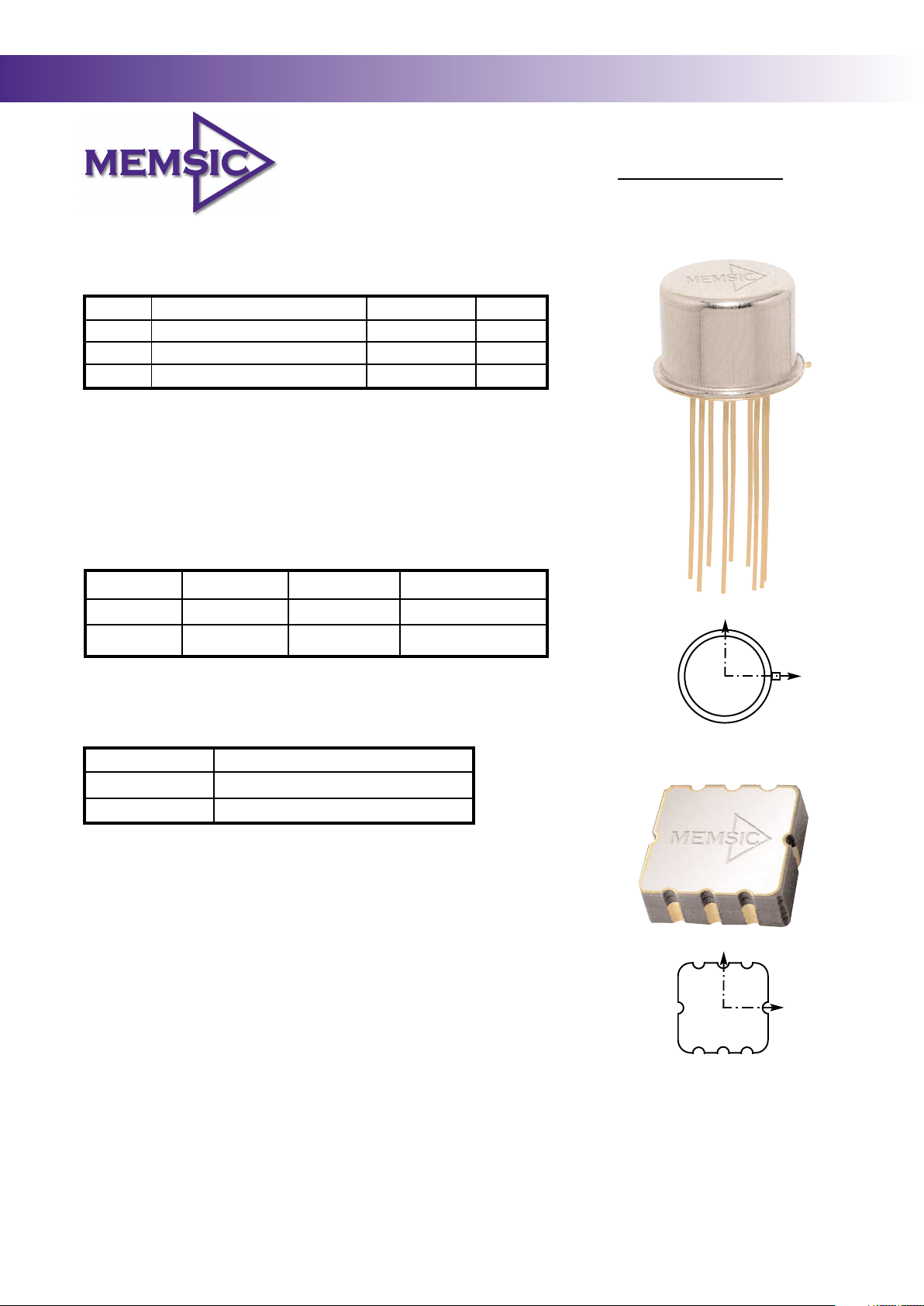
PACKAGE CHARACTERISTICS
Package ThetaJA ThetaJC Device Weight
TO-100 150°C/W 25°C/W 0.04 oz
LCC-8 110°C/W 22°C/W 0.02 oz
Page 3 of 8
®MEMSIC, Inc. 2000.
100 Burtt Road, Andover, MA 01810
Tel: 978.623.8188 • Fax: 978.623.9945
www.memsic.com
MXD205 DIGITAL Data Sheet J 8/1/01
MXD205
TO-100
LCC-8
TO-100
TOP
VIEW
TOP
VIEW
+g
+g
+g
+g
X
X
Y
Y
Axes of Sensitivity
LCC-8
Axes of Sensitivity
ORDERING GUIDE
Model Package Style
MXD205AC TO-100 Metal Can
MXD205AL LCC-8 SMD
*
NOTE
Drops onto hard surfaces can cause shocks of greater than 50,000g
and exceed the absolute maximum rating of the device.
Care should be exercised in handling to avoid damage.
CAUTION
ESD (electrostatic discharge) sensitive device.
*Stresses above those listed under "Absolute Maximum Ratings" may cause permanent damage
to the device. These are stress ratings only; the functional operation of this device at these or any
other conditions above those indicated in the operational sections of this specification is not implied.
Exposure to absolute maximum rating conditions for extended periods may affect device reliability.
ABSOLUTE MAXIMUM RATINGS*
Symbol Parameter Rating Units
VDD Supply Voltage to Ground Potential -0.5 to 7.0 Volts
T
STG
Storage Temperature -65 to +150 Deg C
Acceleration 50,000 g
*
LCC parts are shipped in tape and reel packaging.
Page 4
1
2
3
6
7
8
9
10
5
4
Page 4 of 8
Data Sheet
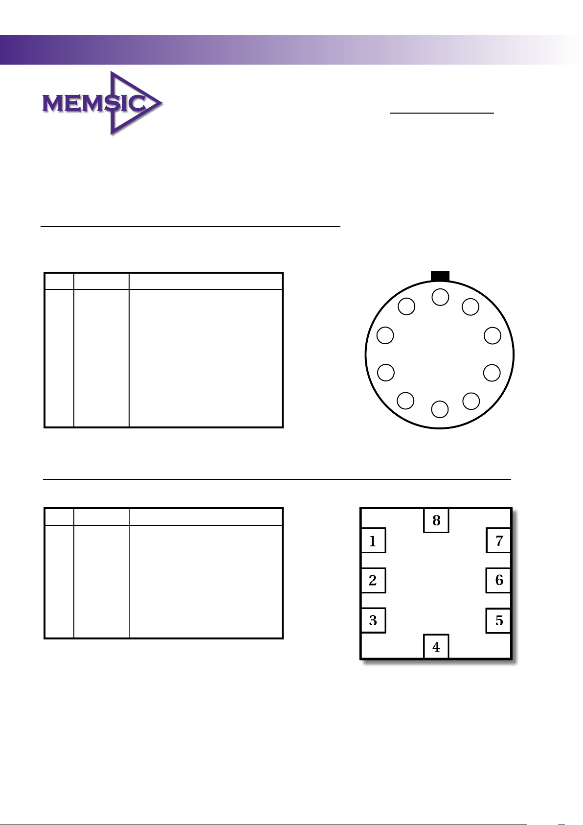
Pin Function Descriptions
TOP-100 and LCC-8
Top View
Top View
®MEMSIC, Inc. 2000.
100 Burtt Road, Andover, MA 01810
Tel: 978.623.8188 • Fax: 978.623.9945
www.memsic.com
MXD205 DIGITAL Data Sheet J 8/1/01
MXD205
Optional external clock factory programmed
per customer request
*
PIN DESCRIPTION: TO -100 Package
Pin Name Description
1 VDD Digital Supply Voltage
2 TOUT Temperature
3 AOUTY Acceleration Signal
4 GND Ground
5 n/c no connection
6 VDA Analog Supply Voltage
7 AOUTX Acceleration Signal
8 VREF 2.50V Reference Voltage
9 SCK Serial Clock
10 n/c no connection
PIN DESCRIPTION: LCC-8 Package
Pin Name Description
1 TOUT Temperature
2 AOUTY Acceleration Signal
3 GND Ground
4 VDA Analog Supply Voltage
5 AOUTX Acceleration Signal
6 VREF 2.50V Reference Voltage
7 SCK Serial Clock
8 VDD Digital Supply Voltage
*
*
Page 5

Page 5 of 8
Data Sheet
Pin Definition
VDD - This is the digital power supply input for the MX20XX. The DC voltage should be between 2.70 and
5.25 volts.
VDA - This is the analog power supply input for the MX20XX. VDA should always be connected to VDD.
GND - This is the ground pin for the MX20XX.
AOUTX - This pin is the output of the x-acceleration sensor.
AOUTY - This pin is the output of the y-acceleration sensor.
TOUT - This pin is the buffered output of the temperature sensor. The voltage at TOUT is an indication of the
die temperature. This voltage can be measured and used to compensate out the temperature dependence of
accelerometer sensitivity.
SCK - Standard product is delivered with an Internal Clock option. Ground this pin when operating with the
Internal Clock. The External Clock must be ordered special from the factory.
VREF - A reference voltage is output from this pin.
®MEMSIC, Inc. 2000.
100 Burtt Road, Andover, MA 01810
Tel: 978.623.8188 • Fax: 978.623.9945
www.memsic.com
MXD205 DIGITAL Data Sheet J 8/1/01
MXD205
Page 6
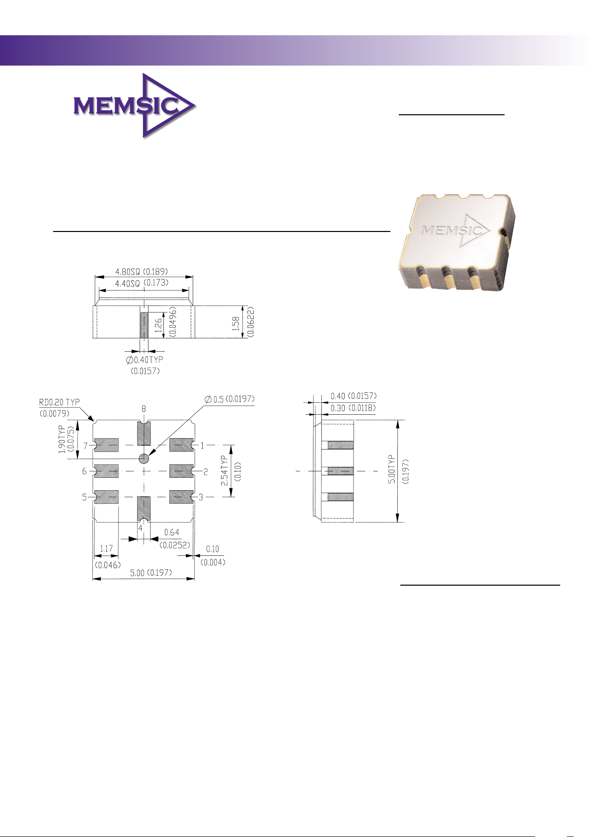
Package Outline
LCC-8 mm (in)
Information furnished by MEMSIC is believed to be
accurate and reliable. However, no responsibility is
assumed by MEMSIC for its use, nor for any infringements of patents or other rights of third parties which
may result from its use. No license is granted by
implications or otherwise under any patent or patent
rights of MEMSIC.
Preliminary technical information.
Subject to change without notice.
Data Sheet
Page 6 of 8
®MEMSIC, Inc. 2000.
100 Burtt Road, Andover, MA 01810
Tel: 978.623.8188 • Fax: 978.623.9945
www.memsic.com
MXD205 DIGITAL Data Sheet J 8/1/01
MXD205
Page 7
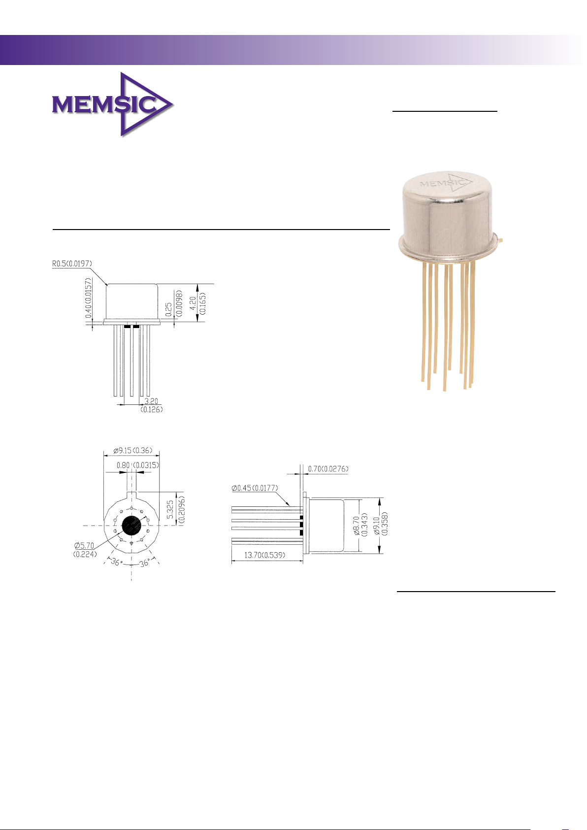
Package Outline
TO-100 mm (in)
Information furnished by MEMSIC is believed to be
accurate and reliable. However, no responsibility is
assumed by MEMSIC for its use, nor for any infringements of patents or other rights of third parties which
may result from its use. No license is granted by
implications or otherwise under any patent or patent
rights of MEMSIC.
Preliminary technical information.
Subject to change without notice.
Data Sheet
Page 7 of 8
®MEMSIC, Inc. 2000.
100 Burtt Road, Andover, MA 01810
Tel: 978.623.8188 • Fax: 978.623.9945
www.memsic.com
MXD205 DIGITAL Data Sheet J 8/1/01
MXD205
Page 8
Information furnished by MEMSIC is believed to be
accurate and reliable. However, no responsibility is
assumed by MEMSIC for its use, nor for any infringements of patents or other rights of third parties which
may result from its use. No license is granted by
implications or otherwise under any patent or patent
rights of MEMSIC.
Technical information.
Subject to change without notice.
Page 8 of 8
Data Sheet
NOTES
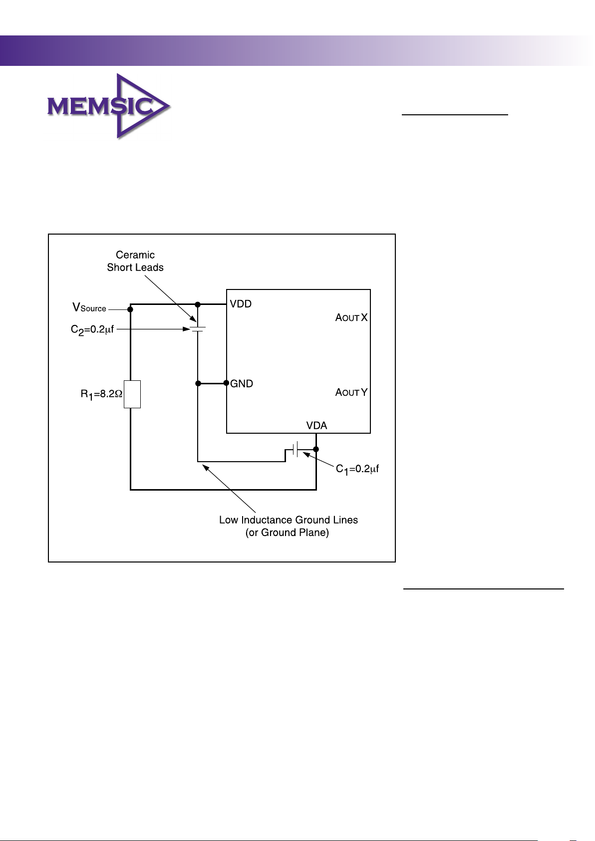
1. Use robust low inductance ground wiring
2. Liberal use of ceramic bypass capacitors
3. The Capacitors should be located as close
as possible to the device supply pins (VDA, VDD).
4. The capacitor lead length should be as short
as possible. Surface mount capacitors are preferred.
Printed Circuit Board Layout and
Fabrication Requirements
®MEMSIC, Inc. 2000.
100 Burtt Road, Andover, MA 01810
Tel: 978.623.8188 • Fax: 978.623.9945
www.memsic.com
MXD205 DIGITAL Data Sheet J 8/1/01
MXD205
 Loading...