

Datasheet MXD1005C-D100, MXD1005C-D150, MXD1005C-D175, MXD1005C-D200, MXD1005C-D250 Datasheet (Maxim)
...Page 1
TAP4
For free samples & the latest literature: http://www.maxim-ic.com, or phone 1-800-998-8800.
For small orders, phone 408-737-7600 ext. 3468.
_______________General Description
The MXD1005 silicon delay line offers five equally
spaced taps with delays ranging from 12ns to 250ns
and a nominal accuracy of ±2ns or ±3%, whichever is
greater. Relative to hybrid solutions, this device offers
enhanced performance and higher reliability, and
reduces overall cost. Each tap can drive up to ten 74LS
loads.
The MXD1005 is available in multiple versions, each
offering a different combination of delay times. It comes
in the space-saving 8-pin µMAX package, as well as an
8-pin SO or DIP, allowing full compatibility with the
DS1005 and other delay line products.
________________________Applications
Clock Synchronization
Digital Systems
____________________________Features
♦ Improved Second Source to DS1005
♦ Available in Space-Saving 8-Pin µMAX Package
♦ 17mA Supply Current vs. Dallas’ 40mA
♦ Low Cost
♦ Delay Tolerance of ±2ns or ±3%, whichever is
Greater
♦ TTL/CMOS-Compatible Logic
♦ Leading- and Trailing-Edge Accuracy
♦ Custom Delays Available
MXD1005
5-Tap Silicon Delay Line
________________________________________________________________
Maxim Integrated Products
1
TAP3
TAP5GND
1
2
87V
CC
TAP1TAP2
TAP4
IN
DIP/SO/µMAX
TOP VIEW
3
4
6
5
MXD1005
14
13
12
11
10
9
8
1
2
3
4
5
6
7
V
CC
N.C.
TAP1
N.C.TAP2
N.C.
N.C.
IN
MXD1005
TAP3
N.C.
TAP5GND
TAP4
N.C.
DIP
_________________Pin Configurations
_____Part Number and Delay Times
19-1309; Rev 0; 10/97
PART
MXD1005C/D__
MXD1005PA__
MXD1005PD__ -40°C to +85°C
-40°C to +85°C
0°C to +70°C
TEMP. RANGE PIN-PACKAGE
Dice*
8 Plastic DIP
14 Plastic DIP
______________Ordering Information
*
Dice are tested at TA= +25°C.
Note: To complete the ordering information, fill in the blank with
the part number extension from the Part Number and Delay
Times table to indicate the desired delay per output.
MXD1005SA__
MXD1005SE__
MXD1005UA__ -40°C to +85°C
-40°C to +85°C
-40°C to +85°C 8 SO
16 Narrow SO
8 µMAX
Pin Configurations continued at end of data sheet.
60 12
PART NUMBER
EXTENSION
(MXD1005_ _ __)
75 15
125
100 20
25
175
150 30
35
250
200 40
50
24
30
40
50
60
70
80
100
36
45
60
75
90
105
120
150
48
60
80
100
120
140
160
200
DELAY (t
PHL
, t
PLH
) PER OUTPUT (ns)
60
75
100
125
150
175
200
250
Note: Contact factory for characterization data.
Functional Diagram appears at end of data sheet.
TAP1 TAP2 TAP3 TAP4 TAP5
Page 2
MXD1005
5-Tap Silicon Delay Line
2 _______________________________________________________________________________________
ABSOLUTE MAXIMUM RATINGS
ELECTRICAL CHARACTERISTICS
(VCC= +5.0V ±5%, TA = -40°C to +85°C, unless otherwise noted. Typical values are at TA= +25°C.) (Note 1)
TIMING CHARACTERISTICS
(VCC= +5.0V ±5%, TA= +25°C, unless otherwise noted.)
Stresses beyond those listed under “Absolute Maximum Ratings” may cause permanent damage to the device. These are stress ratings only, and functional
operation of the device at these or any other conditions beyond those indicated in the operational sections of the specifications is not implied. Exposure to
absolute maximum rating conditions for extended periods may affect device reliability.
Note 1: Specifications to -40°C are guaranteed by design, not production tested.
Note 2: All voltages referenced to GND.
Note 3: Measured with outputs open.
Note 4: I
CC
is a function of frequency and TAP5 delay. Only an MXD1005_ _60 operating with a 40ns period and VCC= +5.25V will
have a maximum I
CC
of 70mA. For example, an MXD1005_ _100 will not exceed 30mA. See Supply Current vs. Input
Frequency graph in
Typical Operating Characteristics.
Note 5: Guaranteed by design.
Note 6: Pulse width and/or period specifications may be exceeded, but accuracy is application sensitive (i.e., layout, decoupling, etc.).
Note 7: VCC= +5V at +25°C. Typical delays are accurate on both rising and falling edges within ±2ns or ±3%.
Note 8: See
Test Conditions
section.
Note 9: The combination of temperature variations from +25°C to 0°C or +25°C to +70°C and voltage variation from 5.0V to 4.75V
or 5.0V to 5.25V may produce an additional typical input-to-tap delay shift of ±1.5ns or ±4%, whichever is greater.
Note 10: All taps and outputs delays tend to vary unilaterally with temperature or supply variations. For example, if TAP1 slows
down, all other taps will also slow down; TAP3 cannot be faster than TAP2.
V
CC
to GND..............................................................-0.5V to +6V
All Other Pins..............................................-0.5V to (V
CC
+ 0.5V)
Short-Circuit Output Current (1sec)....................................50mA
Continuous Power Dissipation (T
A
= +70°C)
8-Pin Plastic DIP (derate 9.1mW/°C above +70°C) ......727mW
14-Pin Plastic DIP (derate 10.0mW/°C above +70°C) ..800mW
8-Pin SO (derate 5.9mW/°C above +70°C)..................471mW
16-Pin Narrow SO (derate 8.7mW/°C above +70°C)....696mW
8-Pin µMAX (derate 4.1mW/°C above +70°C).............330mW
Operating Temperature Range ...........................-40°C to +85°C
Storage Temperature Range.............................-65°C to +160°C
Lead Temperature (soldering, 10sec).............................+300°C
(Note 2)
(Note 2)
(Note 2)
TA= +25°C (Note 5)
0V ≤ VIN≤ V
CC
VCC= 5.25V, period = minimum (Notes 3, 4)
VCC= 4.75V, VOH= 4.0V
VCC= 4.75V, VOL= 0.5V
CONDITIONS
V0.8V
IL
Input Voltage Low
V2.2V
IH
V4.75 5.00 5.25V
CC
Supply Voltage
Input Voltage High
pF5 10C
IN
Input Capacitance
µA-1 1I
L
Input Leakage Current
mA17 70I
CC
Active Current
mA-1I
OH
Output Current High
mA12I
OL
Output Current Low
UNITSMIN TYP MAXSYMBOLPARAMETER
(Notes 7–10)
(Notes 7–10)
(Note 6)
(Note 6)
CONDITIONS
ns
See
Part Number and
Delay Times
table
t
PHL
Input-to-Tap Delay
(trailing edge)
ns
See
Part Number and
Delay Times
table
t
PLH
ns
40% of TAP5
t
PLH
t
WI
Input Pulse Width
Input-to-Tap Delay
(leading edge)
ms100t
PU
Power-Up Time
ns4(tWI)Period
UNITSMIN TYP MAXSYMBOLPARAMETER
Page 3
MXD1005
5-Tap Silicon Delay Line
_______________________________________________________________________________________
3
__________________________________________Typical Operating Characteristics
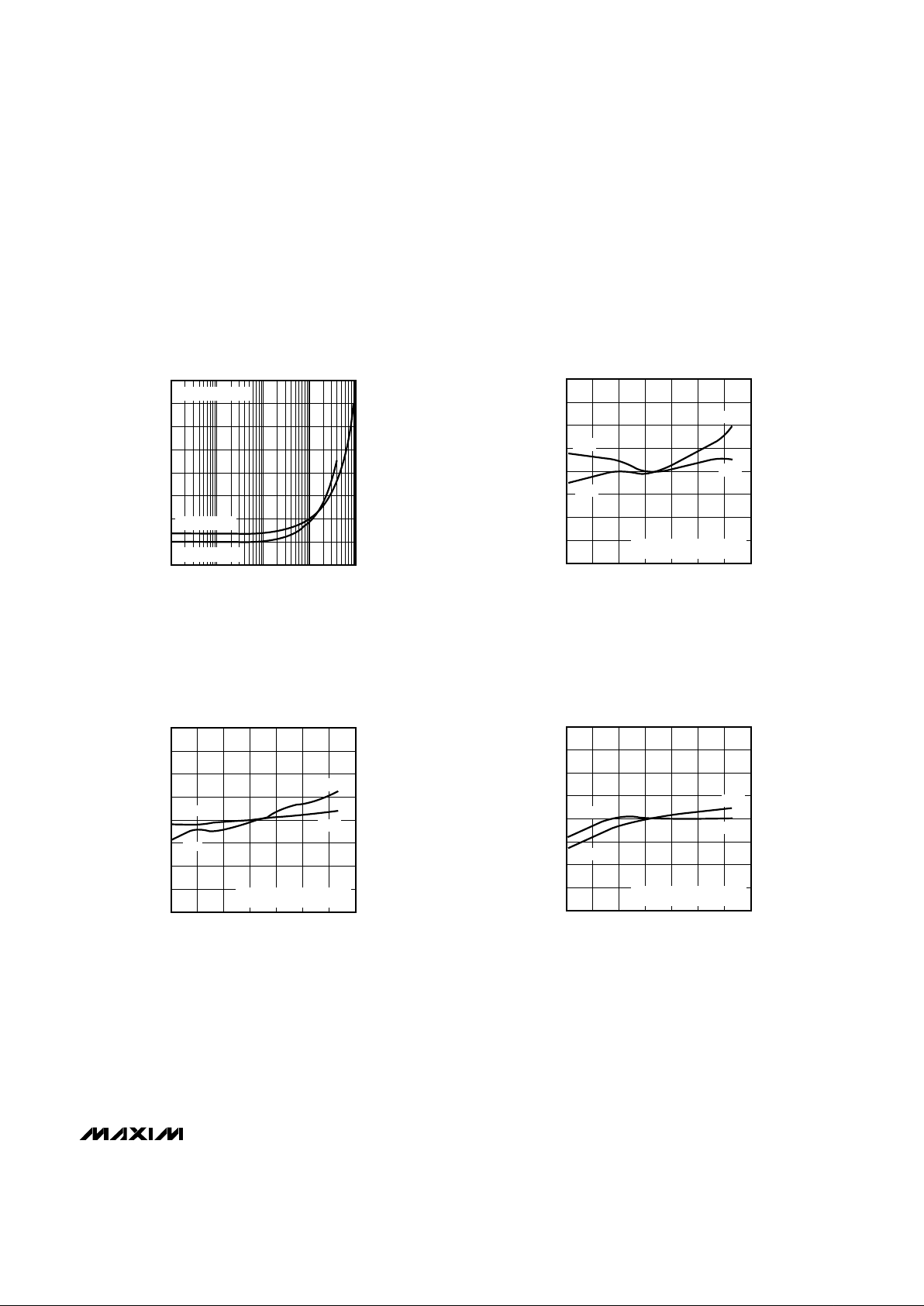
(VCC= +5V, TA= +25°C, unless otherwise noted.)
-2.0
-1.0
-1.5
0
-0.5
1.5
1.0
0.5
2.0
-40 0-20 20 40 60 80 100
MXD1005_ _75
PERCENT CHANGE IN DELAY
vs. TEMPERATURE
MXD1005 TOC1
TEMPERATURE (°C)
% CHANGE IN DELAY (TAP2)
t
PLH
RELATIVE TO NOMINAL (+25°C)
t
PHL
t
PHL
t
PLH
-2.0
-1.0
-1.5
0
-0.5
1.5
1.0
0.5
2.0
-40 0-20 20 40 60 80 100
MXD1005_ _100 TO MXD1005_ _200
PERCENT CHANGE IN DELAY
vs. TEMPERATURE
MXD1005 TOC2
TEMPERATURE (°C)
% CHANGE IN DELAY (TAP2)
t
PHL
RELATIVE TO NOMINAL (+25°C)
t
PHL
t
PLH
t
PLH
-2.0
-1.0
-1.5
0
-0.5
1.5
1.0
0.5
2.0
-40 0-20 20 40 60 80 100
MXD1005_ _250
PERCENT CHANGE IN DELAY
vs. TEMPERATURE
MXD1005 TOC3
TEMPERATURE (°C)
% CHANGE IN DELAY (TAP2)
t
PHL
RELATIVE TO NOMINAL (+25°C)
t
PLH
t
PLH
t
PHL
18
10
11
12
13
14
15
16
17
0.001 0.1 10.01 10
ACTIVE CURRENT
vs. FREQUENCY
MXD1005 TOC4
FREQUENCY (MHz)
ACTIVE CURRENT (mA)
50% DUTY CYCLE
MXD1005_ _75
MXD1005_ _200
Page 4

_______________Definitions of Terms
Period: The time elapsed between the first pulse’s
leading edge and the following pulse’s leading edge.
Pulse Width (tWI): The time elapsed on the pulse
between the 1.5V level on the leading edge and the
1.5V level on the trailing edge, or vice-versa.
Input Rise Time (t
RISE
): The time elapsed between
the 20% and 80% points on the input pulse’s leading
edge.
Input Fall Time (t
FALL
): The time elapsed between
the 80% and 20% points on the input pulse’s trailing
edge.
Time Delay, Rising (t
PLH
): The time elapsed between
the 1.5V level on the input pulse’s leading edge and the
corresponding output pulse’s leading edge.
Time Delay, Falling (t
PHL
): The time elapsed between
the 1.5V level on the input pulse’s trailing edge and the
corresponding output pulse’s trailing edge.
____________________Test Conditions
Ambient Temperature: +25°C ±3°C
Supply Voltage (VCC): +5V ±0.01V
Input Pulse: High = 3.0V ±0.1V
Low = 0.0V ±0.1V
Source Impedance: 50Ω max
Rise and Fall Times: 3.0ns max
Pulse Width: 500ns max
Period: 1µs
Each output is loaded with a 74F04 input gate. Delay is
measured at the 1.5V level on the rising and falling
edges. The time delay due to the 74F04 is subtracted
from the measured delay.
MXD1005
5-Tap Silicon Delay Line
4 _______________________________________________________________________________________
______________________________________________________________Pin Description
1 1 Signal Input
14-PIN DIP
FUNCTION
8-PIN
DIP/SO/µMAX
NAME
16-PIN SO
2 4 40% of specified maximum delay4
1 IN
TAP2
3
PIN
6 80% of specified maximum delay
4 7 Device Ground8
6 TAP4
GND
5 8 100% of maximum specified delay
6 10 60% of specified maximum delay11
9 TAP5
TAP3
7 12 20% of specified maximum delay
8 14 Power-Supply Input16
13 TAP1
V
CC
—
2, 3, 5, 9, 11,
13
No Connection. Not internally connected.
2, 3, 5, 7, 10,
12, 14, 15
N.C.
Note: Maximum delay is determined by the part number extension. See the Part Number and Delay Times table for more information.
Page 5

__________Applications Information
Supply and Temperature
Effects on Delay
Variations in supply voltage may affect the MXD1005’s
fixed tap delays. Supply voltages beyond the specified
range may result with larger variations. The devices are
internally compensated to reduce the effects of temperature variations. Although these devices might vary with
supply and temperature, the delays vary unilaterally,
which suggests that TAP3 can never be faster than
TAP2.
Capacitance and Loading
Effects on Delay
The output load can affect the tap delays. Larger
capacitances tend to lengthen the rising and falling
edges, thus increasing the tap delays. As the taps are
loaded with other logic devices, the increased load will
increase the tap delays.
Board Layout Considerations/Decoupling
The device should be driven with a source that can
deliver the required current for proper operation. A
0.1µF ceramic bypassing capacitor could be used. The
board should be designed to reduce stray capacitance.
MXD1005
5-Tap Silicon Delay Line
_______________________________________________________________________________________ 5
V
IL
V
IH
PERIOD
t
RISE
IN
OUT
0.6V
0.6V
2.4V
2.4V
1.5V
1.5V 1.5V
1.5V
1.5V
t
FALL
t
WI
t
PLH
t
PHL
20%
50Ω
0.1µF
V
CC
IN
(+5V)
20%
TIME
MEASUREMENT
UNIT
TAP1
TAP2
TAP3
TAP4
TAP5
74FO4
20%
20%
20%
MXD1005
Figure 1. Timing Diagram
Figure 2. Test Circuit
Page 6

MXD1005
5-Tap Silicon Delay Line
6 _______________________________________________________________________________________
_________________________________________________________Functional Diagram
___________________Chip Information
TRANSISTOR COUNT: 824
MXD1005
TAP1 TAP2 TAP3 TAP4 TAP5
IN
20% 20% 20% 20% 20%
____Pin Configurations (continued)
TOP VIEW
16
15
14
13
12
11
10
9
1
2
3
4
5
6
7
8
IN V
CC
N.C.
N.C.
TAP1
N.C.
TAP3
N.C.
TAP5
MXD1005
SO
N.C.
N.C.
TAP4
TAP2
N.C.
N.C.
GND
Page 7

MXD1005
5-Tap Silicon Delay Line
_______________________________________________________________________________________ 7
________________________________________________________Package Information
8LUMAXD.EPS
Page 8

MXD1005
5-Tap Silicon Delay Line
Maxim cannot assume responsibility for use of any circuitry other than circuitry entirely embodied in a Maxim product. No circuit patent licenses are
implied. Maxim reserves the right to change the circuitry and specifications without notice at any time.
8
_____________________Maxim Integrated Products, 120 San Gabriel Drive, Sunnyvale, CA 94086 408-737-7600
© 1997 Maxim Integrated Products Printed USA is a registered trademark of Maxim Integrated Products.
___________________________________________Package Information (continued)
SOICN.EPS
 Loading...