

Page 1
P/N: PM0306
1
FEATURES
• Single +5V power supply
• Sigma-Delta A/D D/A with digital filters
• Support u/A Law and 16-bit linear format
• On-chip automatic level control
• On-chip differential line driver
• On-chip digital volume control
• Programmable transmit/receive gain control
• Support switch paths for DAM (Digital Answering
Machine) applications
• Easy interface to general purpose DSPs
• Easy read/write of control register by microprocessors
• Programmable power-down
• Support power-low/battery-low detection
• 28-pin DIP/SOP package
REV. 3.0, JUL 15, 1996
MX93000
MX93000
PRODUCT OVERVIEW
The MX93000 Special Codec integrates key functions
of the analog-front-end of Digital Answering Machine
(DAM) into a single integrated circuit. The MX93000 is
intended to provide a complete, low cost, and single
chip solution for telephone applications requiring a
single +5V power supply.
The MX93000 Special Codec is especially powerful
when applied to some DAM models which are intended
to meet different countries' specifications in the same
system hardware. User can achieve this goal by
simply setting control firmware. This benifit will help
DAM system makers to save developing time and R/D
resources.
The A/D D/A converters are implemented with 2ndorder sigma-Delta modulators. The on-chip digital
filters, which are carried out with 16-bit and 2's
complement format, are used to get the required
frequency response of a PCM Codec. The Codec can
support 8-bit u/A law and linear format. For the latter,
it is 16-bit format with 14-bit resolution .
Before the A/D digitizing the voice-band analog signal
into digital format, the analog signal can be processed
by a built-in Automatic Level Control (ALC) and programmable Gain Amplifier (PGA). The ALC circuit
controls the input level of A/D converter to about 1.5
Volt, so as to get a better signal to noise ratio during a
low-level input. The PGA circuit is used to control the
gain of different sources : microphone, aux or line
input.
After the digital data is converted into analog signal by
the D/A converter, a fully differential line driver is
supported to drive the telephone line directly without
the need of external amplifier. On the other hand, the
analog signal can be monitored by passing the analog
signal to the on-chip volume control circuit, which can
drive an external driver like LM386.
In addition, the MX93000 supports switches and
control registers so that users can program the Special
Codec to be under line operations and all other specific
operations of DAM. To enhance an easy read/write of
control registers by microprocessors, the control data
is clocked by the 8 kHz sampling clock and synchronized by SDEN\, where SDEN\ is coming from the
output port of microprocessor by detecting one of the
rising edge of 8 kHz clock.
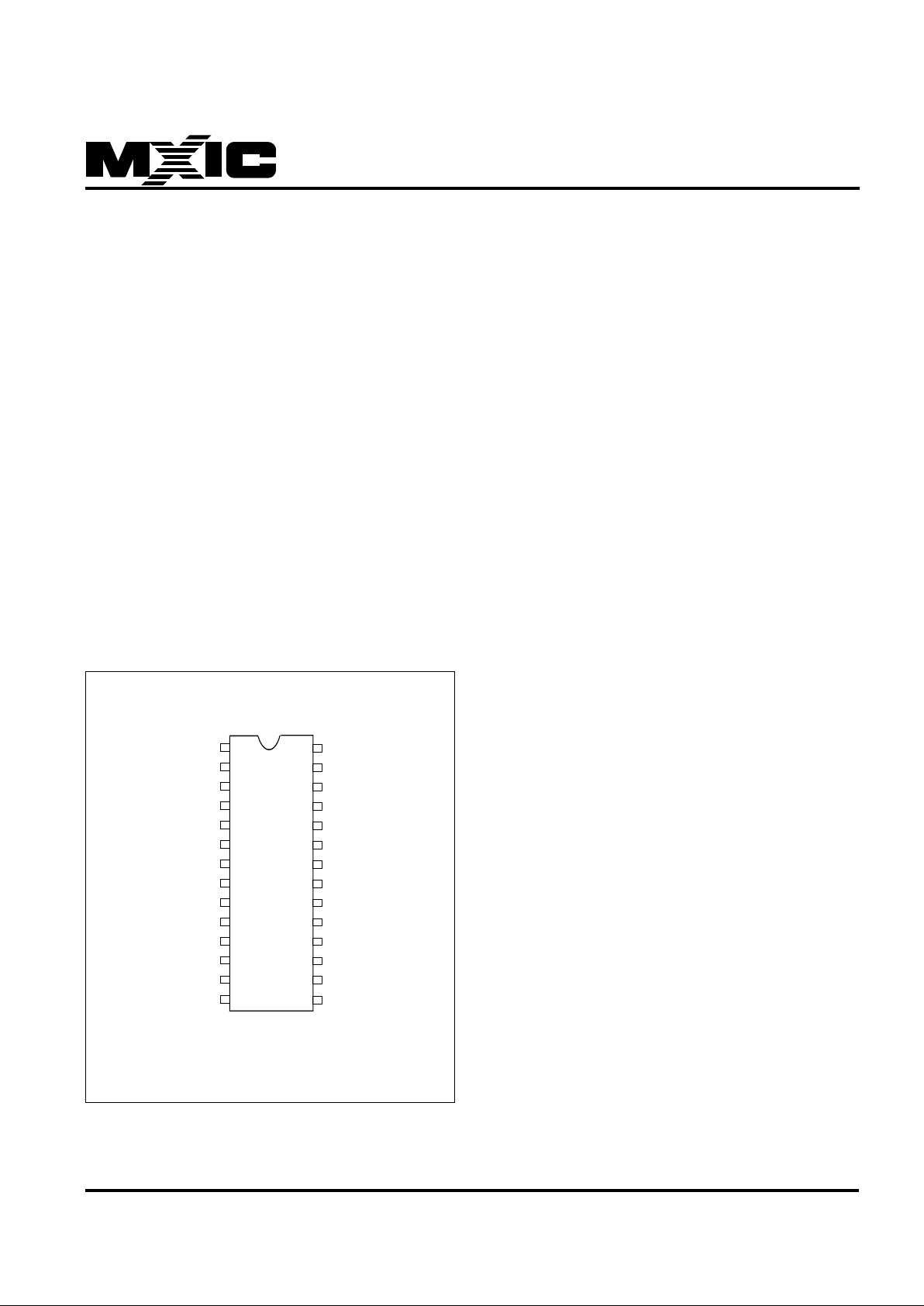
PIN CONFIGURATION
28PIN SOP/DIP
28
27
26
25
24
23
22
21
20
19
18
17
16
15
2
3
4
5
6
7
8
9
10
11
12
13
14
SDATA
SDEN\
DX
DR
FS
MCLK
VDD
GND
PRST
BAT\
VBAT
PDN\
VPOW
LIN
SPK
VR
VREF
FILT
ALCC
ALCRC
PGAC
AUX
MIC
AG
AGND
AVDD
LOUT2
LOUT1
MX93000
1
Page 2
MX93000
MX93000
2
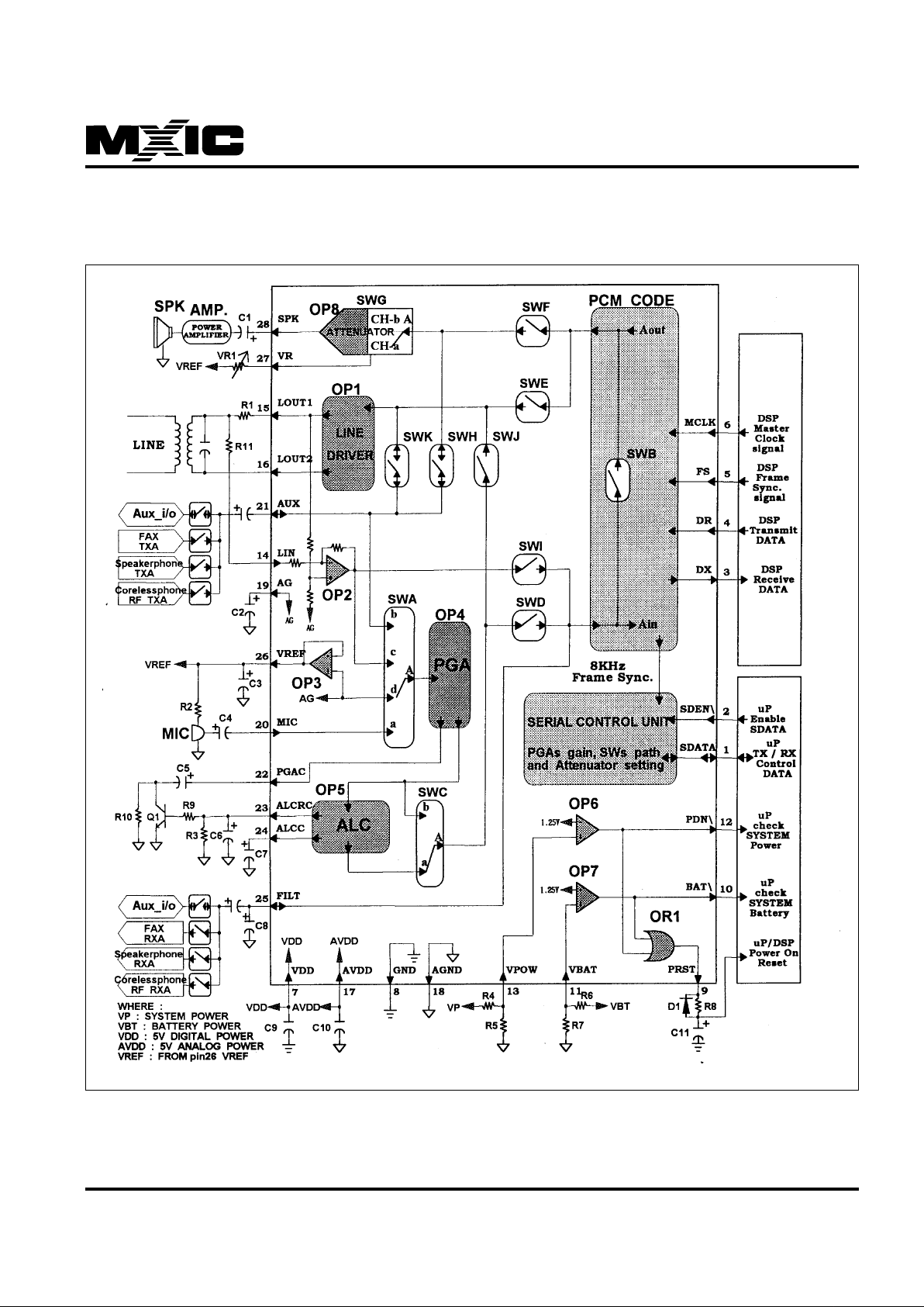
SPECIAL CODEC BLOCK
DIAGRAM
Page 3

MX93000
MX93000
3
PCM CODEC :
This block includes A/D & D/A converters and all of the digital filters.
A/D & D/A converters:
which are implemented with 2nd-order sigma-delta modulation. Output formats are A-Law/u-Law/16-bit linear,
where u/A laws are of CCITT specifications and the 16-bit linear data can get 14-bit resolution and higher linearity
than that of u/A law.
Digital filters :
For the purpose of A/D out-of-band noise filtering and D/A image attenuation, digital filters are implemented on
the same chip.
The digital input applied to D/A converter can not be a dc signal other than idle (bits all zero), as limit cycles in
the digital modulator at a level of -70 dBm will present at the analog output.
POWER MANAGEMENT :
The MX93000 supports the automatic power-down control and power supply detection. This function will work well
even under 3V power supply.
Regarding the power_down procedure please refer to register 4 description for details.
POWER_LOW/BATTERY_LOW detectors : active low
2 comparators and references are used to check whether POWER_LOW/BATTERY_LOW or not. The
relationship between POWER_ON_RESET and POWER_LOW/BATTERY_LOW is as the following table:
(I) POWER_LOW (PDN\) 0 0 1 1
(I) BATTERY_LOW (BAT\) 0 1 0 1
(0)POWER_ON_RESET (PRST) 0 1 1 1
LINE DRIVER :
Not only support the programmable gain from 0 to 22.5 dB with 16 steps and 1.5 dB/step, but also fully differentially
drive -5 dBm power over 300 ohms. If switches SWE , SWJ , and SWK are opened, then the line driver will be
muted to -70dB automatically. In addition, when SWJ or SWK are turned on, there are loss at the line driver output
due to single-ended to fully-differential transform.
LINE_IN BUFFER :
Buffer stage with selection of echo cancellation path or not. For the echo cancellation path, 3-6 dB cancellation
can get it.
PROGRAMABLE GAIN CONTROL (PGA) :
It supports 0 to 22.5 dB gain with 16 steps and 1.5dB/step. The gain value is controlled separately by 3 registers,
where different input signal paths will have a different gain value, and when the input path is changed, the
respective register value will keep no change.
FUNCTIONAL DESCRIPTION
Page 4

MX93000
MX93000
4
AUTOMATIC LEVEL CONTROL (ALC) :
The ALC can support 36 dB gain with the attack time and release time controlled by C6 and R3 * C6, respectively.
SPK ATTENUATOR :
Speaker output signal can be attenuated either by internal register or external resister. For the former, the
attenuation is from 0 to -45 dB with 16 steps and -3.0dB/step. For the later, 10K ohms variable resistor is
suggested. If switches SWF and SWH are open, then attenuator will be muted to -70dB automatically.
SERIAL_CONTROL_INTERFACE :
To read/write the internal registers.
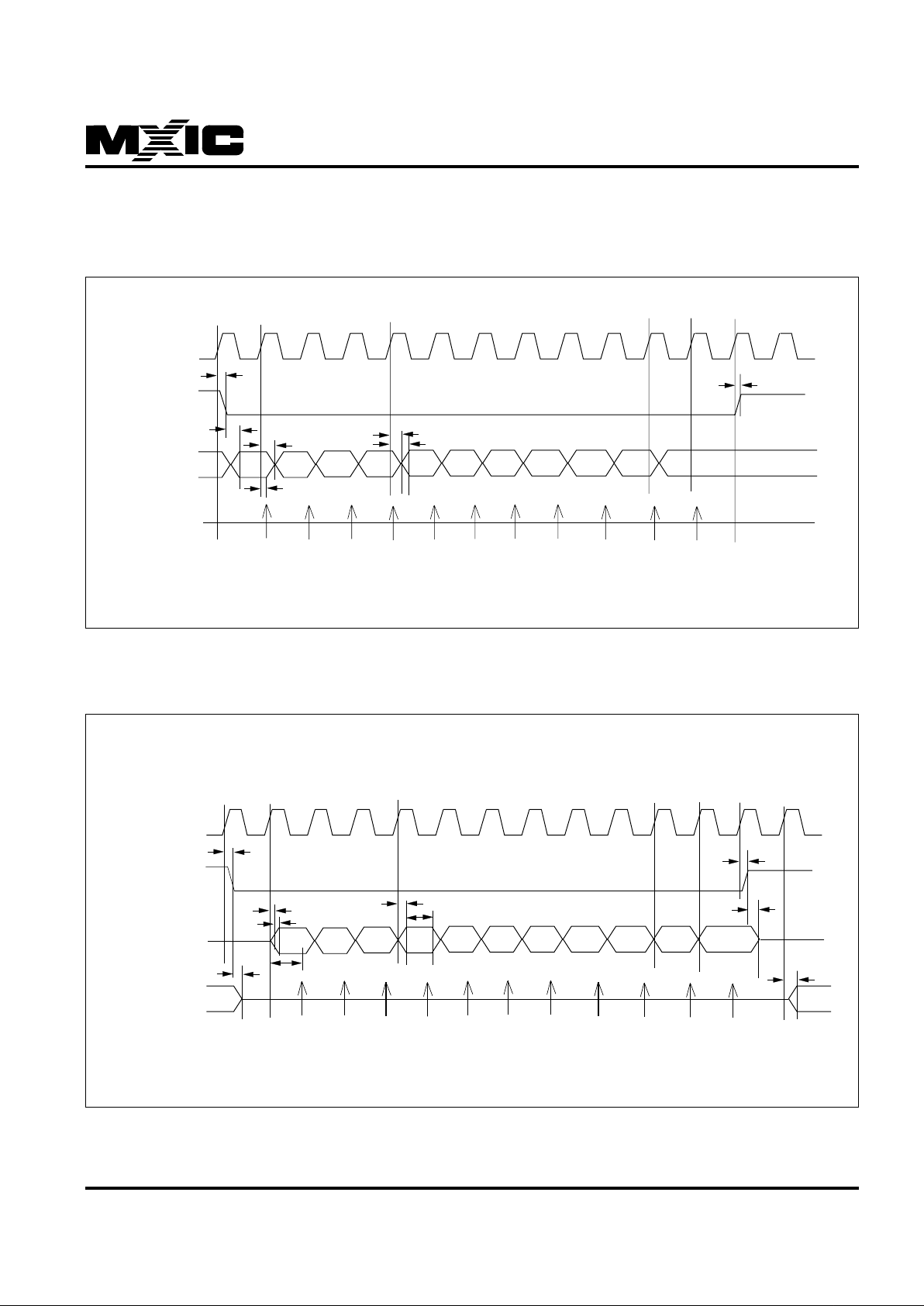
SDEN\ (serial data enable) is used to start receiving control signal.
8kHz frame sync.is used to transmit/receive the serial data (SDATA).
CODEC_SERIAL_PORT :
4-pin signal will complete the data trasmitting/receiving.
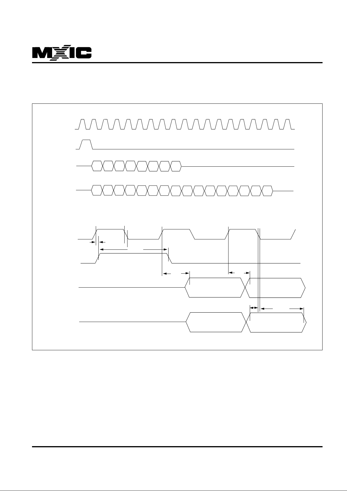
MCLK is not only the data rate but also the chip master clock. Currently, it is fixed at 1.536 MHz and the frame
synchronization clock, Fs, is 8 kHz. For simplicity, the A/D and D/A are synchronous so that MCLK and Fs are
enough.
Data transfer of DX/DR are MSB first in both 8-bit and 16-bit formats.
VOLTAGE REFERENCE :
Two 2.25V voltage references are on-chip generated . VREF is for external and AG is for internal uses. Both two
pins need the decoupling capacitors AGND at all times. VREF can be used to bias the microphone, the level shift
circuits, or others.
SWITCHES :
There are 2 registers which are used to control all of the switches so that user can direct many different signal
paths, of which 3 of them are :
a) Path of normal operation
MIC input --> SWA --> PGA/ALC --> SWC --> SWD --> PCM Codec Ain
LOUT1/LOUT2 <-- LINE DRIVER <-- SWE <-- PCM Codec Aout
b) Path of room monitor
MIC input --> SWA --> PGA/ALC --> SWC --> SWJ --> Line Driver
LINE IN --> Line Buffer --> SWI --> PCM Codec Ain
c) Path of line play
LINE IN --> SWA --> PGA/ALC --> SWC --> SWD --> PCM Codec Ain
LOUT1/LOUT2 <-- Line Driver <-- SWE <-- PCM Codec Aout
SPK <-- Attenuator <-- SWF <-- PCM Codec Aout
Page 5
MX93000
MX93000
5
PARAMETER MIN TYP MAX UNITS
Input Voltage with max S/(N+THD)
MIC/AUX/LINE/FILT 3.4 Vpp
Input Resistance* 15 Kohm
Input Capacitance* 15 pF
ANALOG INPUT
PARAMETER REG.5 D1=0 REG.5 D1=1 UNITS
MIN TYP MAX MIN TYP MAX
Dynamic Range* 36 30 dB
THD*
< 75 mVpp 40 dB
< 1 Vpp 30 dB
< 100 mVpp 40 dB
<1 Vpp 25 dB
PARAMETER MIN TYP MAX UNITS
Gain Range 0 22.5 dB
Step Size 1.3 1.5 1.7 dB
PROGRAMMABLE GAIN AMPLIFIER
SPECIFICATIONS
PARAMETER MIN TYP MAX UNITS
Line Driver:
Gain Range 0.0 22.5 dB
Step Size 1.2 1.5 1.8 dB
Full Swing Output (@600 ohm load)
-- Fully differential(LOUT1-LOUT2) 6.0 Vpp
-- Single Ended (LOUT1) 3.0 Vpp
External Load
-- Resistance* 300 ohm
-- Capacitance* 200 pF
ANALOG OUTPUT
AUTOMATIC LEVEL CONTROL
Page 6

MX93000
MX93000
6
SPK Attenuator :
Gain Range -45 0.0 dB
Step Size -3.5 -3.0 -2.4 dB
Full Swing Output 3.0 Vpp
External Load
-- Resistance* 10 Kohm
-- Capacitance* 100 pF
Mute Attenuation* -70 dB
FILT (I/O)
Input Resistance* 10 Kohm
Output Resistance* 10 Kohm
External Load
-- Capacitance * 1000 pF
AUX (I/O)
Input Capacitance* 15 pF
Input Resistance* 20 Kohm
Output Resistance* 1 Kohm
External Load
-- Capacitance* 100 pF
PARAMETER MIN TYP MAX UNITS
VREF Output 2.0 2.25 2.5 V
VREF Output Current* 800 uA
VOLTAGE REFERENCE
PARAMETER MIN TYP MAX UNITS
Comparator Transfer point 1.10 1.25 1.40 V
Hysteresis* 0.15 V
COMPARATOR DETECTOR
Page 7

MX93000
MX93000
7
PARAMETER MIN TYP MAX UNITS
Dynamic Range (-40 dB FS) 72 dB
THD+N (-6 dB FS) -50 dB
THD+N (u Law) -36 dB
Interchannel Isolation*
Line/AUX/MIC 70 dB
Gain Variation (Note 3) 5 %
Frequency Response
50-60 -25 dB
300-3k -1.0 +1.0 dB
3.2k-3.4k -0.9 +0.25 dB
4K -15 dB
> 4.6 K -32 dB
A/D PATH CHARACTERISTICS (Note 1)
PARAMETER MIN TYP MAX UNITS
Dynamic Range (-40 dB FS) 72 dB
THD+N (-6 dB FS) -50 dB
Gain Variation (Note 3) 5 %
Total Out-of-Band Energy
.6 Fs to 20 KHz -50 dB
Frequency Response
< 300 -0.25 +0.25 dB
300-3k -0.25 +0.25 dB
3.2k-3.4k -0.9 +0.25 dB
4K -15 dB
> 4.6k -32 dB
D/A PATH CHARACTERISTICS (Note 2)
Page 8

MX93000
MX93000
8
PARAMETER MIN TYP MAX UNITS
Idle-channel Noise (Note 4)
-- A/D Path -70 dB
-- D/A Path -70 dB
VDD Power Supply Rejection (Note 5)
-- A/D Channel 40 dB
-- D/A Channel 40 dB
AVDD Power Supply Rejection (Note 5)
-- A/D Channel -50 dB
-- D/A Channel -50 dB
Crosstalk*
-- A/D to D/A (Note 6) -65 dB
-- D/A to A/D (Note 7) -65 dB
NOISE
PARAMETER MIN TYP MAX UNITS
High Level Input Voltage (VIH) 2.0 VDD Volt
Low Level Input Voltage (VIL) 0 0.8 Volt
High Level Output Voltage (VOH) 2.4 VDD Volt
Low Level Output Voltage (VOL) 0.4 Volt
Output Capacitance* 15 pF
Input Capacitance* 15 pF
DIGITAL STATIC SPECIFICATIONS
PARAMETER MIN TYP MAX UNITS
Power Supply - Digital & Analog 4.5 5.5 Volt
Power Supply Current -- Operating
-- Analog (Note 8) 24 mA
-- Digital 6 mA
Power Supply Current -- Power Down 0.6 mA
POWER SUPPLY
Page 9

MX93000
MX93000
9
PARAMETER Symbol MIN MAX UNITS
Supply Voltage VDD-GND -0.3 6.0 Volt
Voltage on any I/O pin GND-0.3 VDD+0.3 Volt
Current on any I/O pin +-8 mA
Operating Ambient Temperature 0 70 °C
Storage Temperature -65 150 °C
Absolute Maximum Ratings
NOTE:
* These items are guaranteed by characterization, not production testing.
1.VDD=AVDD=5.0V, Temp=25°C, Sampling Rate=8KHz, Linear Mode,
fin=1 KHz, Measurement Bandwidth=300--3.4K Hz
A/D Path=MIC --> PGA (0dB) --> A/D, No ALC.
2.VDD=AVDD=5.0V, Temp=25°C, Sampling Rate=8KHz, Linear Mode,
fin=1 KHz, Measurement Bandwidth=300--3.4K Hz
D/A Path=D/A --> SPK (0dB) output
3.Vin=0dB -- -50dB, fin=1KHz.
4. Input is grounded. Measurement Bandwidth=300 -- 3.4K Hz.
5. A/D & D/A input grounded,
Frequency=1KHz, 100m Vp signal on power supply.
6. 0 dB at A/D input, D/A input grounded, then D/A output measured.
7. 0 dB at D/A input, A/D input grounded, then A/D output measured.
8. Power supply current does not include output loading.
Page 10
MX93000
MX93000
10
TIMING DESCRIPTION MIN MAX UNIT
Tfs from Vmckh1 to Vfsh1 0 ns
Tfsh Holding time for Frame Sync. MCLK ns
from Vfsh1 to Vfsh2
Tdxs setting time for Codec Transmit Data 110 ns
from Vmckh1(n) to DX(n) data ready
Tdrh1 Holding time for Codec Receive Data 0 ns
from DR(n) data ready to Vmckh2(n)
Tdrh2 Holding time for Codec Receive Data 150 ns
from Vmckl(n) to DR(n) ending
Tupen1 from Vfsh1 to Venl 40 FS ns
Tupen2 from Vfsh1 to Venh 40 FS ns
Tups1 Setting time for uP/DSP Transmit SDATA 40 FS ns
from Vupenl to uP/DSP SDATA (n) ready
(where Tupen1 + Tups1 must be less than FS)
Tups2 Setting time for uP/DSP Transmit SDATA 40 FS ns
from Vfsh1(n+1) to uP/DSP SDATA (n+1) ready
Tuph Holding time for uP/DSP Transmit SDATA 40 Tups2 ns
from Vfsh1(n+1) to uP/DSP SDATA(n) ending
Tcdrd from Vfsh(n+1) to Codec read SDATA(n) 20 ns
Tupo2i from Vupenl to uP/DSP changing its SDATA interface into 40 FS ns
input port
Tcdi2o from Vfsh1 to Codec changing its SDATA 20 ns
interface into output port
Tcds1 Setting time for Codec Transmit SDATA 20 ns
from Vcdi2o to Codec SDATA(n) ready
Tcds2 Setting time for Codec Transmit SDATA 20 ns
from Vfsh1(n+2) to Codec SDATA(n+1) ready
Tcdh Holding time for Codec Transmit SDATA FS ns
from SDATA(n) ready to Vfsh1(n+2)
Tcdo2i from Venh to Codec changing its SDATA 20 ns
interface into input port
Tuprd from Vfsh1(n+1) to uP/DSP reading SDATA(n) 40 FS ns
Tupi2o from Vfsh1 to uP/DSP changing its SDATA 40 FS ns
interface into output port
SPECIAL CODEC TIMING DESCRIPTION :
Page 11
MX93000
MX93000
11
SPECIAL CODEC TIMING DIAGRAM :
PCM CODEC MASTER CLOCK , FRAME SYNC. & DATA TIMING
MCLK
FS
u-LAW,A-LOW
DR/X
LINEAR
DR/X
1
2
3
4
5
68
7
9
12
345
6
78
12
345
6
78
9101112
14 1513
16
LSB
1
2
1
2
1
2
Tfsh
Tfs
Vmckh1
Vmckh2
Vmckl
Vfsh1
Vfsh2
Vmckh1
Tdxs
(n)
(n+1)
(n)
(n)
(n+1)
(n+1)
Tdxs
Tdrh2
Tdrh1
MCLK
FS
DX
DR
LSB
MSB
MSB
10 11 12 13
14
15
16
Page 12
MX93000
MX93000
12
PCM CODEC CONTROL REGISTER R/W TIMING
CODEC READ SDATA
CODEC WRITE SDATA
FSR/X
SDEN\
uP/DSP SDATA
INTERFACE
CODEC SDATA
INTERFACE
1
23
4
5
678
9
12 13 14
Venl
Tupen1
Tuph
Tups1
A2 A1
A0
D7
D6 D5 D4 D3
D2 D0
D1
Tuph
Tups2
Venh
Tupen2
CODEC
READ SDATA
n
n+1
n+2
10
11
Tcdrd
n n+1
FSR/X
SDEN\
CODEC SDATA
INTERFACE
uP/DSP SDATA
INTERFACE
1
23
4
5
678
9
10
11
12
13 14
Vcdi2o
Tupen1
Tcdo2i
A2 A1
A0
D7
D6 D5 D4 D3
D2 D0
D1
Tupo2i
n
n+1
n+2
Tcds1
Tcdi2o
uP/DSP
READ SDATA
Tcds2
Tcdh
Tupen2
Tupi2o
Vfsh1
Tuprd
n+1
n
Page 13
MX93000
MX93000
13
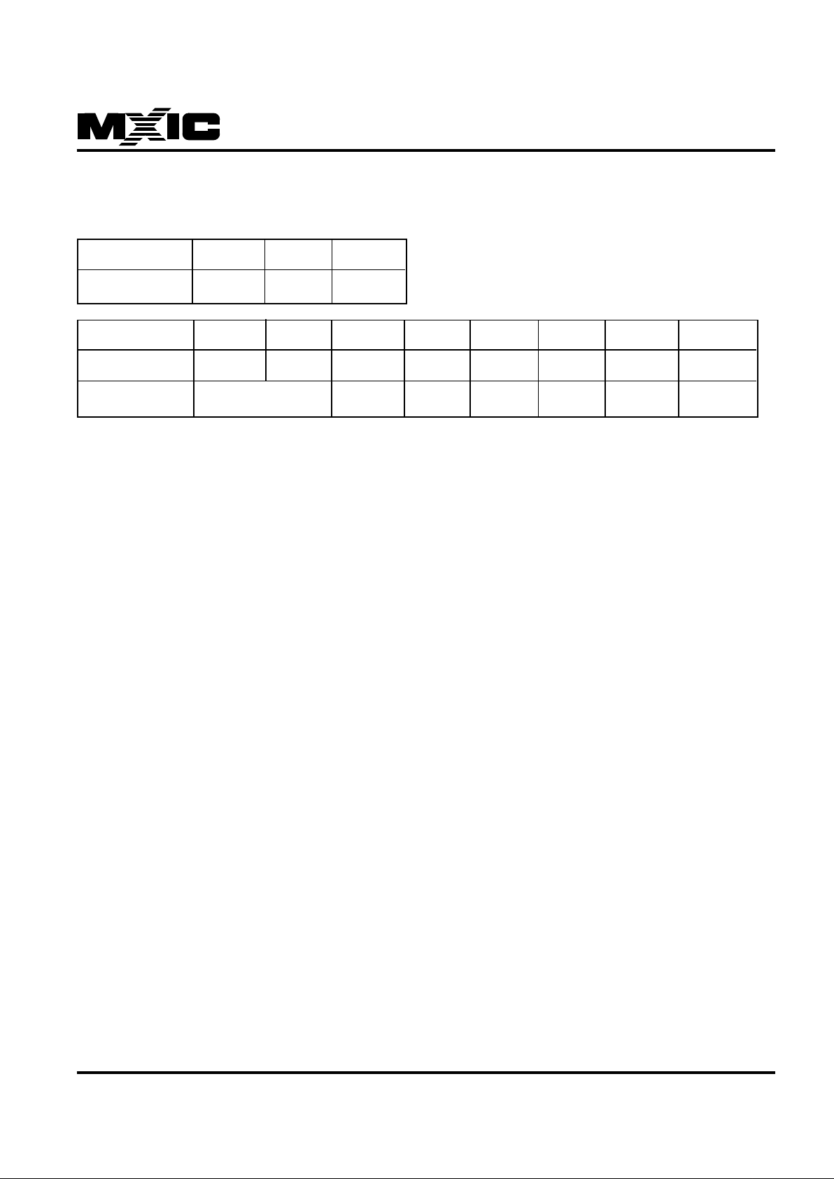
REGISTER 0:
ADDRESS BIT A2 A1 A0
DATA 0 0 0
DATA BIT D7 D6 D5 D4 D3 D2 D1 D0
POWER-ON 0 0 0 0 0 0 0 0
DESCRIPTION SWA-CTL SWB-CTL SWC-CTL SWD-CTL SWE-CTL SWF-CTL SWG-CTL
REGISTERS DEFINITION :
(SWA-CTL) D(7,6) = (1,1) : path of SWA is "c==>A"
PGA setting following LINE-IN GAIN SETTING
= (1,0) : path of SWA is "b==>A"
PGA setting following AUX-IN GAIN SETTING (see Note 1.)
= (0,1) : path of SWA is "a==>A"
PGA setting following MIC-IN GAIN SETTING
= (0,0) : path of SWA is "d==>A" (grounding to AG)
(SWB-CTL) D(5) = (1) : path of SWB is "CLOSE"
= (0) : path of SWB is "OPEN"
(SWC-CTL) D(4) = (1) : path of SWC is "b==>A"
= (0) : path of SWC is "a==>A"
(SWD-CTL) D(3) = (1) : path of SWD is "CLOSE"
= (0) : path of SWD is "OPEN"
(SWE-CTL) D(2) = (1) : path of SWE is "CLOSE"
= (0) : path of SWE is "OPEN"
(SWF-CTL) D(1) = (1) : path of SWF is "CLOSE"
= (0) : path of SWF is "OPEN"
(SWG-CTL) D(0) = (1) : path of SWG (ATTENUATOR) is "A==>b"
ATTENUATOR setting following ALARM-OUT SETTING
= (0) : path of SWG (ATTENUATOR) is "A==>a"
ATTENUATOR adjusted by external VR1
Page 14
MX93000
MX93000
14
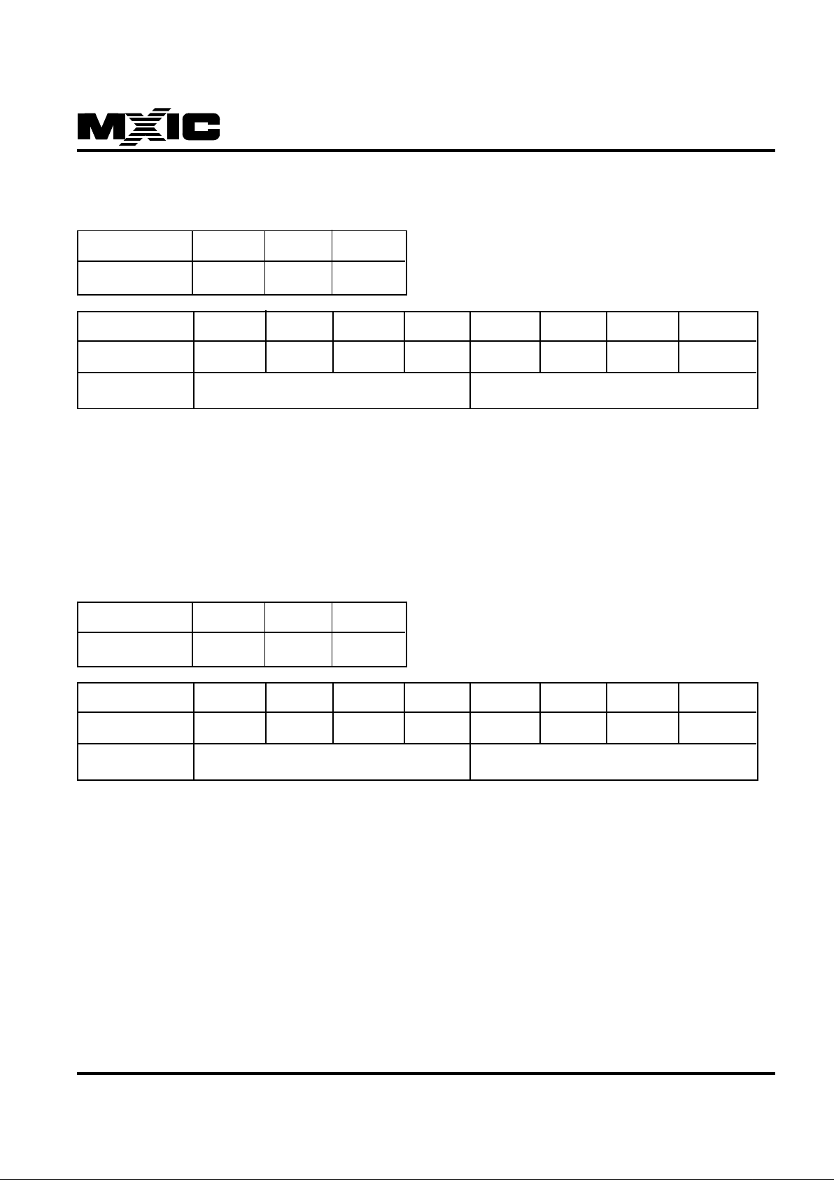
REGISTER 1 :
ADDRESS BIT A2 A1 A0
DATA 0 0 1
DATA BIT D7 D6 D5 D4 D3 D2 D1 D0
POWER-ON 0 0 0 0 0 0 0 0
DESCRIPTION LINE-IN GAIN SETTING LINE-OUT GAIN SETTING
(AUX-IN GAIN SETTING) D(7-4) = (F) - (0) : 22.5dB - 0dB, 1.5dB/STEP
(MIC-IN GAIN SETTING) D(3-0) = (F) - (0) : 22.5dB - 0dB, 1.5dB/STEP
REGISTER 2 :
ADDRESS BIT A2 A1 A0
DATA 0 1 0
DATA BIT D7 D6 D5 D4 D3 D2 D1 D0
POWER-ON 0 0 0 0 0 0 0 0
DESCRIPTION AUX-IN GAIN SETTING MIC-IN GAIN SETTING
(LINE-IN GAIN SETTING) D(7-4) = (F) - (0) : 22.5dB - 0dB, 1.5dB/STEP
(LINE-OUT GAIN SETTING) D(3-0) = (F) - (0) : 22.5dB - 0dB, 1.5dB/STEP
Page 15
MX93000
MX93000
15
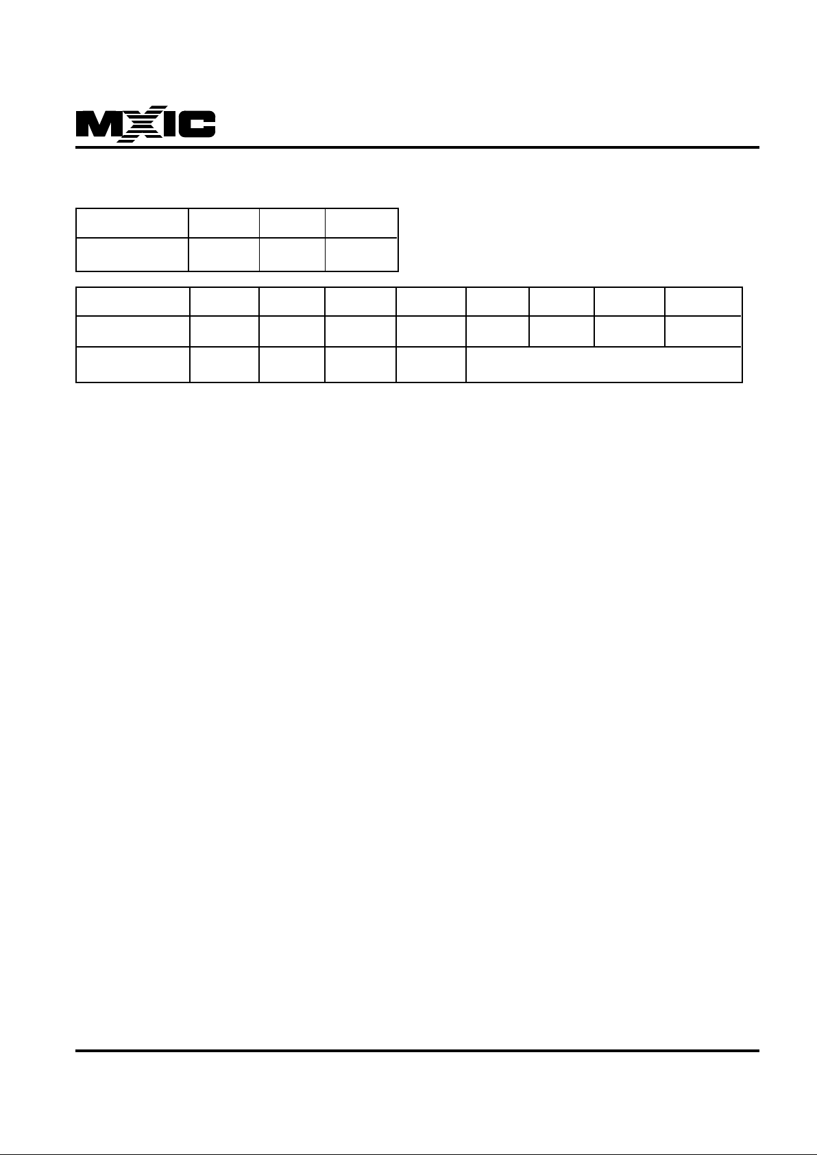
REGISTER 3 :
ADDRESS BIT A2 A1 A0
DATA 0 1 1
DATA BIT D7 D6 D5 D4 D3 D2 D1 D0
POWER-ON 0 0 0 0 1 1 1 1
DESCRIPTION SWH-CTL SWI-CTL SWJ-CTL SWK-CTL ALARM-OUT ATTENUATOR SETTING
(SWH-CTL) D(7) = (1) : path of SWH is "CLOSE"
= (0) : path of SWH is "OPEN" (see Note 1.)
(SWI-CTL) D(6) = (1) : path of SWI is "CLOSE"
= (0) : path of SWI is "OPEN"
(SWJ-CTL) D(5) = (1) : path of SWJ is "CLOSE"
= (0) : path of SWJ is "OPEN"
(SWK-CTL) D(4) = (1) : path of SWK is "CLOSE"
= (0) : path of SWK is "OPEN" (see Note 1.)
(ALARM-OUT ATTENUATOR SETTING) D(3-0) = (F) - (0) : -45dB - 0dB 3dB/STEP
where ALARM-OUT ATTENUATOR ==> ATTENUATOR CHANNEL-b
SPK-OUT ATTENUATOR ==> ATTENUATOR CHANNEL-a (adjusted by VR1 10Ký)
Page 16
MX93000
MX93000
16
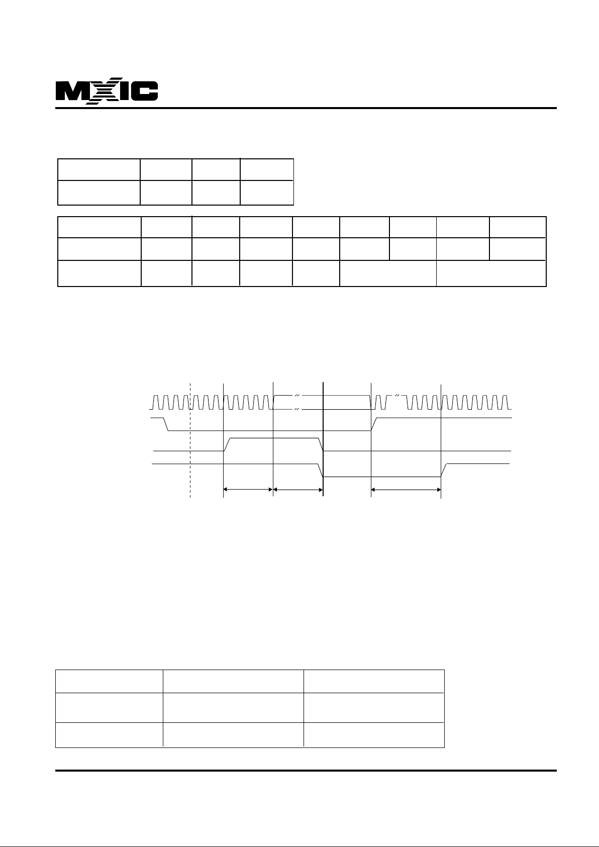
DATA BIT D7 D6 D5 D4 D3 D2 D1 D0
POWER_ON 0 0 0 0 0 0 0 0
DESCRIPTION PDN ECHO MASTER CLOCK CODEC FORMAT
REGISTER 4 :
ADDRESS BIT A2 A1 A0
DATA 1 0 0
(PDN) D(6)=1 : POWER DOWN MODE.
a.When D(6) is set to 1, the MX93000 will enter power down mode after 5 MCLKS.
The 5_MCLK period is for the initialization of digital circuits in the MX93000.
b.When the MX93000 enters power down mode, it will clear all registers after 20us.
c.When system power recovers and MCLK is enabled, the MX93000 will wake up
after 30ms and then user can restore all registers.
SIGN\SCALE MIN MAX
POSITIVE 0000 0000 0000 0000 0111 1111 1111 1100
NEGATIVE 1111 1111 1111 1100 1000 0000 0000 0000
LINEAER 16 BITS FORMAT : 14 BITS RESOLUTION with 2LSB=0
(ECHO) D(5) = (1):ECHO CANCELLER ON (3-6dB)
(0):ECHO CANCELLER OFF
(MASTER CLOCK) D(3,2) = (0,0): 1.536 MHz
(CODEC FORMAT) D(1,0) = (1,1): LINEAR CODER & DECODER (16 BITS FORMAT)
= (1,0): LINEAR CODER & DECODER (16 BITS FORMAT)
= (0,1): A-LAW CODER & DECODER (8 BITS FORMAT)
= (0,0): u-LAW CODER & DECODER (8 BITS FORMAT)
MCLK (pin 6)
PDN\ (pin12)
REG4 PDN bit
CODEC
power-consumption
> 5 MCLKs
20 us
30 ms
MCLK Keep Hi or Low
CKTs power_on
up set PDN = 1
Page 17
MX93000
MX93000
17
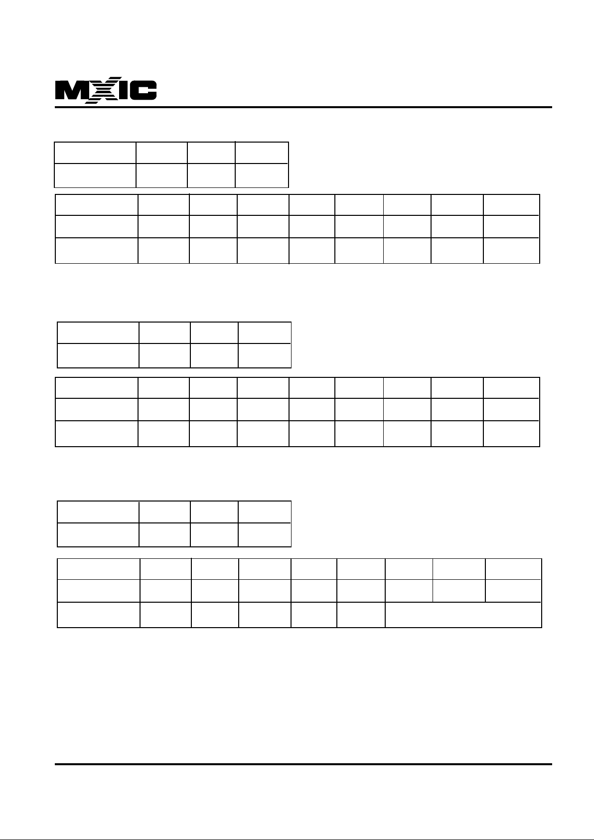
REGISTER 5 :
ADDRESS BIT A2 A1 A0
DATA 1 0 1
DATA BIT D7 D6 D5 D4 D3 D2 D1 D0
POWER-ON 0 0 0 0 0 0 0 0
DESCRIPTION ALC
(ALC) D(1) = 1 : ALC loop gain attenuate 6dB
D(1) = 0 : ALC loop gain attenuate 0dB
REGISTER 6 :
ADDRESS BIT A2 A1 A0
DATA 1 1 0
@@ reserve for internal use
DATA BIT D7 D6 D5 D4 D3 D2 D1 D0
POWER-ON 0 0 0 0 0 0 0 0
DESCRIPTION
@@ reserve for future use
DATA BIT D7 D6 D5 D4 D3 D2 D1 D0
POWER-ON 0 0 0 0 0 0 0 0
DESCRIPTION READ REGISTER ADDRESS
REGISTER 7 :
ADDRESS BIT A2 A1 A0
DATA 1 1 1
(READ) D(3) = 1 : read data from register 0-6
= 0 : write data to register 0-7
(REGISTER ADDRESS) D(2-0) :
1.When READ = 1, READ will be cleared automatically.
2.When READ = 1, next uP/DSP SDEN\ signal active low, CODEC will change CODEC SDATA interface into
output and following the last time REGISTER ADDRESS to output the content of register.
Note 1. :When using SWK or SWH, the path between AUX and SWA will disconnect. Oppositely, if using the path
between AUX and SWA, then SWK and SWH will be invalid.
Page 18
MX93000
MX93000
18
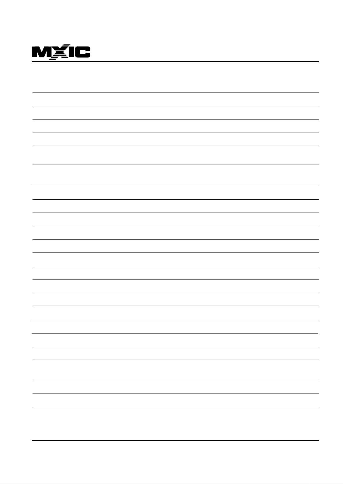
REFERANCE PART DESCRIPTION
R1 620 ý matching resistor; to reflect 600ý at the transformer primary
R2 2 Ký current-limit resistor; to limit MIC bias current ; please follow MIC specification
R3 75 Ký time constant ; ALC release time constant = R3 * C6
R4,R5 to scale down SYSTEM power supply (VPOW) and compare with 1.25V to
do power-down check
R6,R7 to scale down BATTERY (VBAT) and compare with 1.25V to do power-down
check
R8 10Ký the time constant for power-on-reset circuits ; where RC=R8 * C11
R9 10 Ký current-limit resistor for Q1
R10 330 Ký discharge path for ALC circuit when Q1 turns off
R11 200 Ký to attenuate line-in signal
C1,C4 0.1 uF DC blocking capacitor
C2,C3 10 uF to decouple analog virtual ground ; where AG = VREF = 2.25v
C5 10 uF DC blocking capacitor
C6 47 uF time constant ; ALC Attack time contant > 2ký ± 10% * C6
C7 1uF DC offset cancellation decouple capacitor
C8 1000 pF anti-aliasing capacitor
C9 0.1 uF decoupling capacitor for power supply of Codec digital circuit
C10 0.1 uF decoupling capacitor for power supply of Codec analog circuit
C11 10 uF the time constant for power-on-reset circuits ; where RC = R8 * C11
VR1 10Ký to attenuate the input signal from SWH or SWF ; if using digital volume control,
then connecting pin-27 VR to VREF
Q1 2N3904 ALC feedback component ; all NPN (ß > 100) transistor can play this role
D1 1N4148 to protect reset circuits from spike
THE FOLLOWING LIST IS BASIC COMPONENT REQUIRED :
Page 19
MX93000
MX93000
19
PIN DESCRIPTIONS :
SYMBOL PIN TYPE PIN NUMBER DESCRIPTION
SDATA I/O(D) 1 Bidirectional serial port ; It's an interface for microprocessor
serial data transfer
SDEN\ I (D) 2 Serial data enable ; active low ; for starting to receive/transmit
serial data (A2-D0)
DX O (D) 3 Transmit data pin (Codec serial data)
DR I (D) 4 Receive data pin (Codec serial data)
FS I (D) 5 Codec frame sync ; 8KHz frame synchronization clock for the
transmit/receive channel
MCLK I (D) 6 Master clock input (MCLK=1.536 MHz)
When this pin is continuously high or low and set register4/bit-
6
"PDN=1", then the MX93000 will enter power-down mode
VDD (D) 7 Digital power ; 5V power supply for all internal digital logic
GND (D) 8 Digital ground ; ground reference (0V) for all internal digital
logic
PRST O (D) 9 Power on reset (active high) ; Determined by PDN\ and BATT\
input signal
BAT\ O (A) 10 Battery detector output (active low); referenced to 1.25V
VBAT I (A) 11 Battery detector input ; the voltage is divided from battery
power for reference to 1.25V
PDN\ O (A) 12 Power down detector output (active low) ; referenced to 1.25V
VPOW I (A) 13 Power down detector input ; System DC power is divided and
then connected so as to compare with reference voltage
(1.25v)
LIN I (A) 14 Telephone signal line input , can be switched to PGA.
LOUT1 O (A) 15 Telephone line output (postive) with PGA ; where PGA gain is
from 0 to 22.5dB
LOUT2 O (A) 1 6 Telephone line output (negative) with PGA ; where PGA gain
is from 0 to 22.5dB
Note : "D" means digital
"A" means analog
Page 20
MX93000
MX93000
20
SYMBOL PIN TYPE PIN NUMBER DESCRIPTION
AVDD (A) 17 Analog power supply ; 5V power for all internal analog circuitry
AGND (A) 18 Analog ground ; ground reference(0V) for all internal analog
circuitry
AG O (A) 19 Internal analog ground ; nominal 2.25V and must not be used
to sink or source current
MIC I (A) 20 Microphone signal input, can be switched to PGA, where PGA
gain is from 0 to 22.5dB
AUX I/O (A) 21 1.Auxiliary signal input, can be switched to PGA, where PGA
gain is from 0 to 22.5dB
2.As an output port for Aout or an input port for attenuator or
line driver
PGAC O (A) 22 Programmable Gain Amplifier output port
ALCRC O (A) 2 3 Auto level control time constant ; where RC=2K±10%*C6
ALCC O (A) 24 Offset cancellation capacitor (positive) ; normally add a 1 uF
capacitor
FILT I/O (A) 25 1.Anti-aliasing filter; normally add a 1000pF capacitor
2.As an input port for Codec or an output port for SWD or SWI
VREF O (A) 26 Voltage reference ; normal 2.25V and can sink 500uA
VR 0 (A) 27 Speaker volume control ; use a variable resistor 10ký
SPK O (A) 28 Speaker output ; it can be attenuated by VR or control register
from 0 to -45dB
Page 21

MX93000
MX93000
21
APPENDIX :
MX93000 Buglist
1.A/D Full Swing :
Full Swing of A/D is 3.4 Volt in stead of the original target 3.0 Volt.
2.Maximum External Attenuation of SPK through VR pin is only 27 dB.
3.Line Drive Gain:
Line driver will behave as a gain loss rather than a gain loss rather than a gain stage whenever line driver inputs
are come from SWK and/or SWJ.
Line Driver gain if input from
SWE SWK/SWJ
0.0 dB -9.0 dB
1.5 dB -8.7 dB
3.0 dB -7.6 dB
4.5 dB -6.8 dB
6.0 dB -6.0 dB
7.5 dB -5.3 dB
9.0 dB -4.6 dB
10.5 dB -4.0 dB
12.0 dB -3.5 dB
13.5 dB -3.0 dB
15.0 dB -2.6 dB
16.5 dB -2.2 dB
18.0 dB -1.9 dB
19.5 dB -1.6 dB
21.0 dB -1.4 dB
22.5 dB -1.2 dB
4.The larger of VREF's bypass capacitor, the better of D/A idle channel noise.
100 uF rather than 10uF can get a good performance.
Page 22
MX93000
MX93000
22
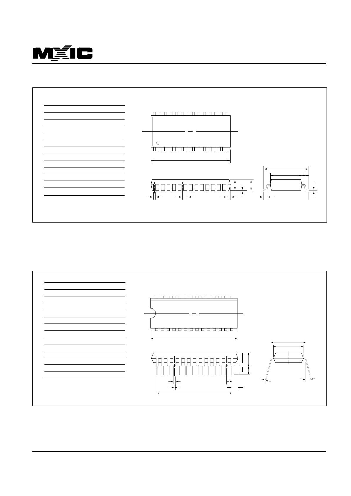
ITEM MILLIMETERS INCHES
A 17.83 max. .702 max.
B 1.194 max. .026 max.
C 1.27 [TP] .047 [TP]
D .41 [Typ.] .016 [Typ.]
E .20 min. .008 min.
F 2.54 max. .100 max.
G 2.34 ± .13 .092 ± .005
H 10.31 ± .31 .406 ± .012
I 7.60 ± .13 .299 ±.005
J 1.37 ± .20 .054 ± .008
K .25 [Typ.] .010 [Typ.]
L .91 ± .20 .036 ± .008
28-PIN PLASTIC SOP (300 mil)
NOTE: Each lead centerline is located within .25
mm[.01 inch] of its true position [TP] at a
maximum material condition.
114
1528
A
DC B
E
GF
L
K
JI
H
28-PIN PLASTIC DIP (300 mil)
NOTE: Each lead centerline is located within .25
mm[.01 inch] of its true position [TP] at a
maximum material condition.
ITEM MILLIMETERS INCHES
A 34.29 max 1.350 max
B .64 [REF] .025 [REF]
C 2.54 [TP] .100 [TP]
D .46 [Typ.] .018 [Typ.]
E 32.99 1.300
F 1.52 [Typ.] .060 [Typ.]
G 3.30 ± .25 .130 ± .010
H .51 [REF] .020 [REF]
I 3.30 ± 2.5 .130±.098
J 3.81 max. .150 max.
K 7.87 ± 2.5 .310±.098
L 7.32 ± 2.5 .288±.098
M .25 [Typ.] .010 [Typ.]
IJ
HG
B
C
F
D
E
A
1
14
K
L
M
2~8°
15
28
Page 23

MX93000
MX93000
23
ORDERING INFORMATION
MX 93 000 K C
COMMERICIAL 0 ~ 70×C
MXIC
COMPONY
PREFIX
FAMILY
PREFIX
PRODUCT NUMBER
PACKAGE TYPE
K:PDIP
S:SOP
Page 24

MX93000
MX93000
24
MACRONIX INTERNATIONAL CO., LTD
HEADQUARTERS :
TEL : +886-3-578-8888
FAX : +886-3-578-8887
EUROPE OFFICE :
TEL : +32-2-456-8020
FAX : +32-2-456-8021
JAPAN OFFICE :
TEL : +81-44-246-9100
FAX : +81-44-246-9105
SINGAPORE OFFICE :
TEL : +65-747-2309
FAX : +65-748-4090
TAIPEI OFFICE :
TEL : +886-2-2509-3300
FAX : +886-2-2509-2200
MACRONIX AMERICA INC.
TEL : +1-408-453-8088
FAX : +1-408-453-8488
CHICAGO OFFICE :
TEL : +1-847-963-1900
FAX : +1-847-963-1909
http : //www.macronix.com
MACRONIX INTERNATIONAL CO., LTD. reserves the right to change product and specifications without notice.
 Loading...