

Page 1
DATA BULLETIN
MX803A
Audio Signaling Processor
Features Applications
Full Duplex Audio Signaling Processor
•
Single Tone
Selective Call systems
Tone Decoder with programmable
•
NOTONE timer.
Two Individual tone encoders and a
•
programmable TX Period Timer.
Low Power CMOS Device
•
On-Chip programmable amplifier.
•
C-BUS Compatible
•
SIGNAL INPUT BIAS
(RX)
AUDIO IN
V
DD
V
BIAS
V
SS
XTAL/
CLOCK
XTAL
AUDIO SWITCH IN
CLOCK
GENERATOR
DIGITAL
NOISE
FILTER 1
PROGRAMMABLE
(TX PERIOD)
TIMER
AUDIO
SWITCH
RX FILTER
SWITCH
DIGITAL
NOISE
FILTER 2
TONE 1
GENERATOR
5-/2-TONE
DTMF 1
V
BIAS
TONE 2
GENERATOR
CUES/DTMF 2
_
+
SUMMING
AMPLIFIER
Signaling Systems supported
•
SelCall (CCIR, EEA, ZVEI I / II /III)
2-Tone SelCall
DTMF Encode
Inband Tone Signaling capability for
•
LMR and other Radio Systems.
QUALITY
METER
GATE TIME
GENERATOR
FREQUENCY
COUNTER
PROGRAMMABLE
NOTONE
TIMER
CUES
CAL
SUMMING
SWITCH
CAL/CUES
SWITCH
PRELIMINARY INFORMATION
COMMAND DAT A
REPLY DATA
C-BUS
AND
LOGIC
LOW
LOW
CHIP SELECT
INTERRUPT
SERIAL CLOCK
LOGIC INPUT
TONE 1 OUT
SUM IN
SWITCHED SUM OUT
SUM OUT
CAL/CUES OUT
TONE 2 OUT
SWITCH OUT
INTERF ACE
CONTROL
PASS
FILTER
PASS
FILTER
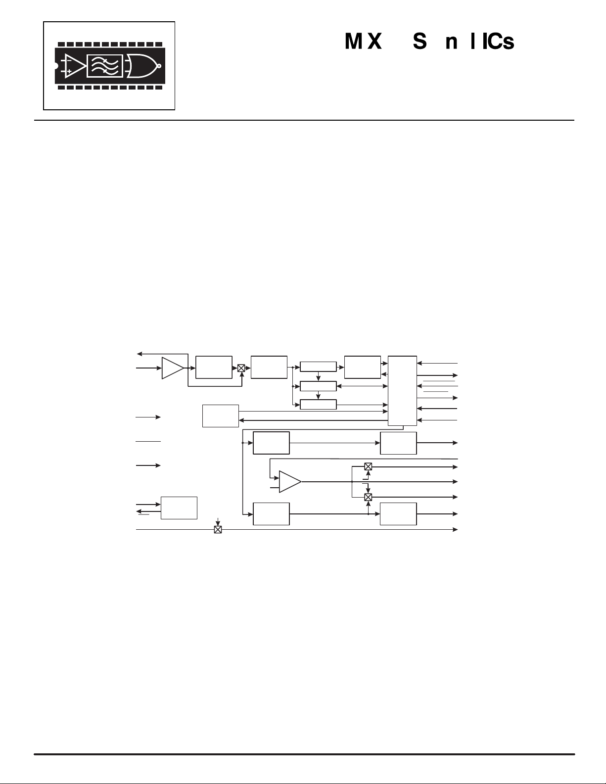
The MX803A is an audio signaling processor that provides inband tone signaling capabilities for LMR and other Radio
systems. A low-power CMOS device, the MX803A is a member of the DBS800 (Digitally integrated Baseband Subsystem) IC family (See section 4.2). Supported Signaling systems include SelCall (CCIR, EEA, ZVEI I, II, and III) 2-Tone
SelCall and DTMF encode. The use of a non-predictive decoder and a versatile encoder, allows the MX803A to operate
in any standard or non-standard tone system.
The MX803A is a full-duplex device for use with Single Tone or Selective Call systems. The MX803A consists of a tone
decoder with a programmable NOTONE timer, two individual tone encoders and a programmable TX period timer, and an
on-chip summing amplifier. Under the control of a µC, the MX803A will simultaneously encode and transmit 1 or 2 audio
tones in the 208-3000Hz range, as well as detect, decode, and indicate the frequency of any non-predicted input tone in
the frequency range of 313 to 6000Hz.
The MX803A is available in 24-pin CDIP (MX803AJ), 24-pin PLCC (MX803ALH), and 24-pin SOIC (MX803ADW)
packages.
1996 MX•COM, INC. Tele: 800 638 5577 910 744 5050 Fax: 910 744 5054 Doc. # 20480122.003
Page 2

Audio Signaling Processor 2 MX803A PRELIMINARY INFORMATION
CONTENTS
Section Page
1. Block Diagram.................................................................................................................................. 3
2. Signal List......................................................................................................................................... 4
3. External Components...................................................................................................................... 6
4. General Description......................................................................................................................... 7
4.1 DESCRIPTION.......................................................................................................................................... 7
4.2 DBS800 Systems...................................................................................................................................... 7
4.3 C-BUS Control .......................................................................................................................................... 8
5. Application ....................................................................................................................................... 8
5.1 MX803A Internal Registers....................................................................................................................... 8
5.2 Address/Commands.................................................................................................................................. 9
5.3 Powersave ............................................................................................................................................... 18
5.4 Interrupt Request
5.5 Operational Recommendations................................................................................................................ 19
5.6 General Reset.......................................................................................................................................... 20
.............................................................................................................................. 19
IRQ
6. Timing Information.......................................................................................................................... 20
7. Performance Specification............................................................................................................. 22
7.1 Electrical Performance............................................................................................................................. 22
7.2 Packaging ................................................................................................................................................ 25
MX•COM, Inc. reserves the right to change specifications at any time and without notice.
1996 MX•COM, INC. Tele: 800 638 5577 910 744 5050 Fax: 910 744 5054 Doc. # 20480122.003
Page 3
Audio Signaling Processor 3 MX803A PRELIMINARY INFORMATION
1. Block Diagram
SIGNAL INPUT BIAS
(RX)
AUDIO IN
V
DD
DIGITAL
NOISE
FILTER 1
PROGRAMMABLE
(TX PERIOD)
TIMER
RX FILTER
SWITCH
DIGITAL
NOISE
FILTER 2
QUALITY
METER
GATE TIME
GENERATOR
FREQUENCY
COUNTER
PROGRAMMABLE
NOTONE
TIMER
C-BUS
INTERFACE
AND
CONTROL
LOGIC
COMMAND DATA
REPLY DATA
CHIP SELECT
INTERRUPT
SERIAL CLOCK
LOGIC INPUT
V
BIAS
V
SS
XTAL/
CLOCK
CLOCK
GENERATOR
XTAL
AUDIO SWITCH IN
AUDIO
SWITCH
TONE 1
GENERATOR
5-/2-TONE
DTMF 1
_
V
BIAS
+
SUMMING
AMPLIFIER
TONE 2
GENERATOR
CUES/DTMF 2
Figure 1: Block Diagram
CUES
CAL
SUMMING
SWITCH
CAL/CUES
SWITCH
LOW
PAS S
FILTER
LOW
PAS S
FILTER
TONE 1 OUT
SUM IN
SWITCHED SUM OUT
SUM OUT
CAL/CUES OUT
TONE 2 OUT
SWITCH OUT
1996 MX•COM, INC. Tele: 800 638 5577 910 744 5050 Fax: 910 744 5054 Doc. # 20480122.003
Page 4

Audio Signaling Processor 4 MX803A PRELIMINARY INFORMATION
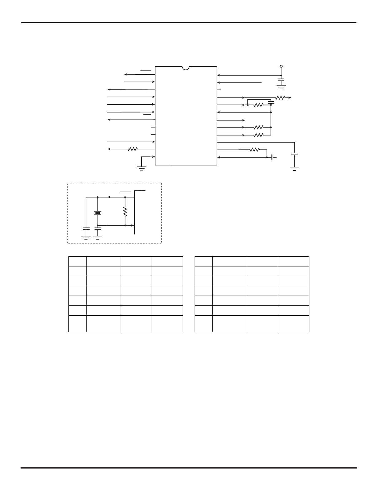
2. Signal List
Pin No. Name Type Description
1
XTAL
2 Xtal/Clock Input Input to the on-chip clock oscillator inverter. A Xtal or externally derived clock
3 Reply Data Output
4
CS
5 Command Data Input
6 Logic Input Input This “real-time” input is available as a general purpose logic input port which
7
IRQ
10 Audio Switch In Input Input to the stand-alone on-chip Audio Switch. This function is
11 Audio Switch Out Output Output of the stand-alone on-chip Audio Switch..
12 V
SS
13 Rx Audio In Input Received audio tone signaling input. This input must be ac coupled and
14 Signal Input Bias Input External components are required between this input and the RX Audio In pin.
15 V
BIAS
16 Tone 1 Out Output Tone 1 Generator (2-/5-tone Selcall or DTMF 1) output. External gain and
17 Tone 2 Out Output Tone 2 Generator (2-/5-tone Selcall, CUES or DTMF 2) output. External gain
Output Output of the on-chip clock oscillator. External components are required at this
output when a Xtal is used. See Figure 2.
should be connected here. See Figure 2.
C-BUS serial data output to the µC. The transmission of Reply Data bytes is
synchronized to the Serial Clock under the control of the Chip Select input.
This 3-state output is held at high impedance when not sending data to the µC.
See Figure 8 and Figure 9.
Input
C-BUS data loading control function. This input is provided by the µC. Data
transfer sequences are initiated, completed or aborted by the chip select signal.
See Figure 8 and Figure 9.
C-BUS serial data input from the µC. Data is loaded to this device in 8-bit
bytes, MSB (B7) first and LSB (B0) last, synchronized to the Serial Clock. See
Figure 8 and Figure 9.
can be read from the Status Register. See Table 3.
G/Purpose Timer Period Expired
NOTONE Timer Period Expired
RX Tone Measurement Complete
These interrupts are inactive during relevant powersave conditions and can be
disabled by bits 5 and 6 in the Control Register.
Output
Output of this pin indicates an interrupt condition to the µC by going to a logic
“0.” This is a “wire-or-able” output, allowing the connection of up to 8
peripherals to 1 interrupt port on the µC. This pin has a low impedance
pulldown to logic “0” when active and a high impedance when inactive. The
system IRQ line requires one pullup resistor to V
. The conditions that cause
DD
interrupts are indicated in the Status Register and are shown below:
enabled/disabled by Bit 7 of the Control Register
Power Negative supply (GND).
connected, using external components, to the Signal Input Bias pin. See Figure
2.
See Figure 2.
Output Internal circuitry bias signal, held at VDD/2. This pin should be decoupled to V
SS
by capacitor C2. See Figure 2..
coupling components are required at this output when operating in a complete
DBS 800 audio installation. The frequency of this output is determined by
writing to the TX Tone Generator 1 Register (Table 5). See Figure 2.
and coupling components are required at this output when operating in a
complete DBS 800 audio installation. The frequency of this output is
determined by writing to the TX Tone Generator 2 Register (Table 5).
See Figure 2.
1996 MX•COM, INC. Tele: 800 638 5577 910 744 5050 Fax: 910 744 5054 Doc. # 20480122.003
Page 5

Audio Signaling Processor 5 MX803A PRELIMINARY INFORMATION
Pin No. Name Type Description
18 CAL/CUES Out Output An auxiliary, selectable tone frequency output, providing a square wave
CALibration signal from the Tone 2 Generator or a sine wave CUES (beep)
signal from the Summing Amplifier. The output mode (CAL or CUES) is
selected by Bit 14 in the TX Tone Generator 2 Register (Table 5). When Tone
Generator 2 is set to Notone, the CAL input is pulled to V
powersave of Tone Generator 2 it is held at V
SS
.
; during a
BIAS
19 Sum in Input Input to the on-chip Summing Amplifier. This amplifier is available for
combining Tone 1 and Tone 2 outputs (DTMF). Gain and coupling components
should be used at this input to provide the required system gains. See Figure 2
and Figure 3
20 Sum Out Output Output of the on-chip summing amplifier. Combined tones (1 and 2) are
available at this output. See Figure 2 and Figure 3.
21 Switched Sum
Out
Output This is the combined tone output available for transmitter modulation. The
switch allows control of the MX803A output. Control of this switch is by Bit 4 of
the Control Register. See Figure 2 and Figure 3.
23 Serial Clock Input
C-BUS serial clock input. This clock, produced by the µC, is used for transfer
timing of commands and data to and from the MX803A. See Figure 8 and
Figure 9.
24 V
DD
Power Positive supply. A single +5 volt power supply is required. Levels and voltages
within this Audio Signaling Processor are dependent upon this supply..
8, 9, 22 N/C No Internal Connection. These pins may be connected to VSS to improve
screening and reduce noise levels around the MX803A.
1996 MX•COM, INC. Tele: 800 638 5577 910 744 5050 Fax: 910 744 5054 Doc. # 20480122.003
Page 6
Audio Signaling Processor 6 MX803A PRELIMINARY INFORMATION
3. External Components
V
DD
V
SEE INSET
BELOW
XTAL/CLOCK
REPLY DATA
COMMAND DATA
LOGIC INPUT
AUDIO SWITCH IN
AUDIO SWITCH OUT
R
7
XTAL
CS
IRQ
V
1
2
3
4
5
6
MX803A
7
8
9
10
11
SS
12
BIAS
24
SERIAL CLOCK
23
22
SWITCHED SUM OUT
21
SUM OUT
20
SUM IN
19
CAL/CUES OUT
18
TONE 2 OUT
17
TONE 1 OUT
16
V
BIAS
15
SIGNAL BIAS
14
RX AUDIO IN
13
C
6
R
6
C
R
4
R
5
R
2
5
TONE LEVEL
AND GAIN
COMPONENTS
C
1
C
2
R
3
INSET
C
4
C
R1
R2
R3 Note 2, 3
R4 Note 2, 3
R5 Note 2, 3
R6 Note 2
R7 Note 2, 5
R
X
1
XTAL/CLOCK
3
XTAL
1
1.0M
2.0M
100k
82.0k
122k
100k
100k
1
MX803A
2
Ω
Ω
Ω
Ω
Ω
Ω
Ω
±10% C1
±10% C2
0.1µF
1.0µF
±20%
±20%
±10% C3 Note 4 33.0pF ±20%
±10% C4 Note 4 33.0pF ±20%
±10% C5 Note 3 22.0pF ±20%
±10% C6
1.0µF
±20%
±10% X1 Note 1, 4 4.00MH
z
Figure 2: Recommended External Components
Notes:
1. Xtal/clock components described are recommended in accordance with MX-COM's Application Note on Standard and
DBS 800 Crystal Oscillator Circuits (April 1990). For best results, a crystal oscillator design should drive the clock
inverter input with signal levels of at least 40% of V
, peak to peak. Tuning fork crystals generally cannot meet this
DD
requirement. To obtain crystal oscillator design assistance, consult your crystal manufacturer.
2. System Components whose values are calculated to allow the MX803A to operate with other DBS 800 microcircuits.
Figure 3 shows these components used in the system signal paths.
3. R3, R4, R5 and C5 are tone mixing components calculated to provide a 3dB tone differential (twist) for use in a DTMF
configuration. Single tone output levels are set independently.
4. When X1 > 5.00MHz, C3 = C4 = 18pF
5. R7 provides modulation level and matching outputs for the MX803A.
1996 MX•COM, INC. Tele: 800 638 5577 910 744 5050 Fax: 910 744 5054 Doc. # 20480122.003
Page 7
Audio Signaling Processor 7 MX803A PRELIMINARY INFORMATION
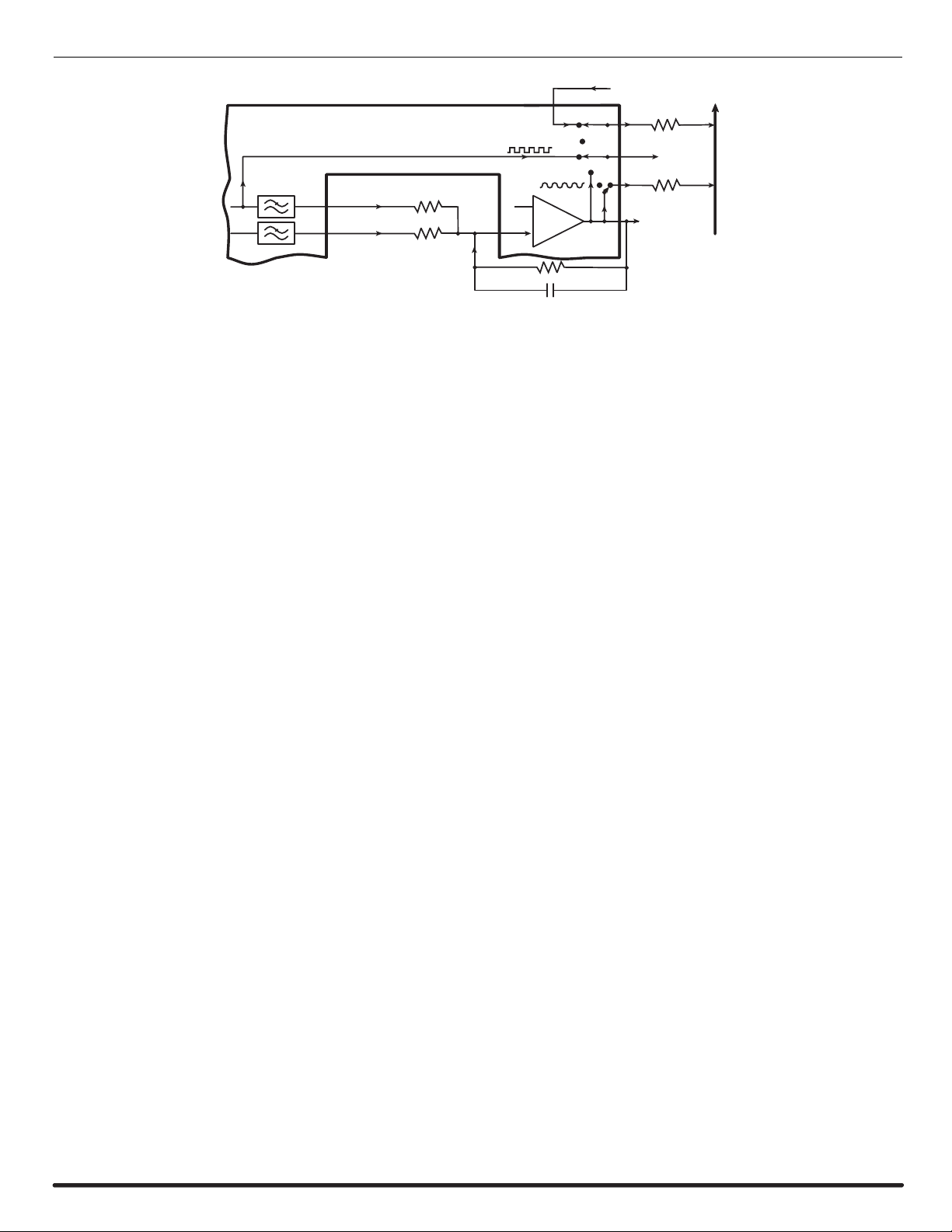
FROM MX806A
CUES
MAIN PROCESS OUT
AUDIO SWITCH OUT
11
18
CAL/CUES OUT
21
SWITCHED SUM OUT
SUM OUT
20
AUDIO SWITCH IN
MX803A
TONE 2 OUT
17
16
TONE 1 OUT
Figure 3: Example of Signal Switching in a DBS800 microcircuit
SUM IN
BIAS
19
10
+
_
CAL
SUMMING
AMPLIFIER
TO MX806A
CALIBRATION IN
TO MX806A
SUM IN
DBS 800 TRANSMIT A UDIO BUS
4. General Description
4.1 DESCRIPTION
The MX803A is an audio signaling processor that provides inband tone signaling capabilities for LMR and other Radio
systems. A low-power CMOS device, the MX803A is a member of the DBS800 (Digitally integrated Baseband Subsystem) IC family (See section 4.2). Supported Signaling systems include SelCall (CCIR, EEA, ZVEI I, II, and III) 2-Tone
SelCall and DTMF encode. The use of a non-predictive decoder and a versatile encoder, allows the MX803A to operate
in any standard or non-standard tone system.
The MX803A is a full-duplex device for use with Single Tone or Selective Call systems. The MX803A consists of a tone
decoder with a programmable NOTONE timer, two individual tone encoders and a programmable TX period timer, and an
on-chip summing amplifier. Under the control of a µC, the MX803A will simultaneously encode and transmit 1 or 2 audio
tones in the 208-3000Hz range, as well as detect, decode, and indicate the frequency of any non-predicted input tone in
the frequency range of 313 to 6000Hz.
A general purpose logic input, interfacing directly with the Status Register, is provided. This may be used as an auxiliary
method of routing digital information to the µC via C-BUS. Output frequencies are produced from data loaded to the
MX803A. A programmable, general purpose, on-chip timer sets the tone transmit periods. A Dual-Tone Multi-Frequency
(DTMF) output is obtained by combining the 2 independent output frequencies in the integral summing amplifier. This
process can also be used for level correction.
Tones produced by the MX803A can be used in the system as modulation calibration inputs and as “CUE” audio
indications to the operator. Received tones are measured and their frequency indicated to the µC in the form of a
received data word. A poor quality or incoherent tone will indicate Notone.
4.2 DBS800 Systems
The Digitally-Integrated Baseband Subsystem (DBS800) is a family of low power ICs which provide a comprehensive
range of audio processing and signaling functions for use within LMR and other Radio Systems. Each DBS800 IC may
be used as part of a complete audio system, or each IC may operate as a stand alone. The system and ICs are
partitioned in such a way that radio designers can easily select the device or devices appropriate to their needs.
The DBS800 family consists of the following ICs:
4.2.1 MX802 DVSR Codec
This is a full-duplex CVSD speech encoder/decoder with the ability to store and retrieve data within attached DRAM
(Dynamic Random Access Memory) using an on-chip DRAM controller. The MX802 also provides on-chip input and
output audio filtering.
4.2.2 MX803A Audio Signaling Processor
This provides an inband tone signaling ability to LMR and other Radio Systems.
1996 MX•COM, INC. Tele: 800 638 5577 910 744 5050 Fax: 910 744 5054 Doc. # 20480122.003
Page 8
Audio Signaling Processor 8 MX803A PRELIMINARY INFORMATION
4.2.3 MX805A Sub-Audio Signaling Processor
This provides a sub-audio and digital signaling (NRZ) ability to LMR and other Radio Systems.
4.2.4 MX806A Audio Processor
This is a half duplex audio processor providing all DBS800 system audio signal conditioning and filtering capabilities for
the system transmit and receive paths.
4.2.5 MX809 MSK Modem
This is an intelligent, half-duplex 1200bps MSK/FFSK Modem with software programmable byte-synchronization system
and checksum generation and checking.
4.2.6 MX812 VSR Codec
This is a half-duplex CVSD speech encoder/decoder with the ability to store and retrieve data within attached DRAM
(Dynamic Random Access Memory) using an on-chip DRAM controller
4.3 C-BUS Control
C-BUS is the controlling hardware and software interface for all members of the DBS800 family. It enables the serial, bidirectional transfer of commands and data throughout the system, allowing total flexibility of operational control and data
handling. System upgrades can be achieved by a simple software or firmware change.
The C-BUS physically consist of 5 lines. These lines are Serial Clock, Command Data, Reply Data, Chip Select (
and Interrupt Request (
). A description of each may be found in section 2.
IRQ
CS),
5. Application
Control of the MX803A Audio Signaling Processor's operation is by communication between the µC and the MX803A
internal registers on the C-BUS using Address/Commands (A/Cs) and appended instructions or data. See Figure 8. The
use and content of these instructions is detailed in the following sections.
For additional application information contact MX•COM, Inc.
5.1 MX803A Internal Registers
Write only, control and configuration of the MX803A.
Control Register
Status Register
RX Tone Frequency Register
RX Notone Timer
TX Tone Generator 1 Register
TX Tone Generator 2 Register
General Purpose Timer Register
30
H
Read only, reporting of device functions.
31
H
Read only, indicates frequency of the last received input.
32
H
Write only, setting of the RX Notone period.
33
H
Write only, setting the required output frequency from TX Tone Generator 1.
34
H
Write only, setting the required output frequency from TX Tone Generator 2.
35
H
Write only, setting of a general purpose sequential time period.
36
H
1996 MX•COM, INC. Tele: 800 638 5577 910 744 5050 Fax: 910 744 5054 Doc. # 20480122.003
Page 9

Audio Signaling Processor 9 MX803A PRELIMINARY INFORMATION
5.2 Address/Commands
The first byte of a loaded data sequence is always recognized by the C-BUS as an Address/Command (A/C) byte.
Instruction and data transactions to and from this device consist of an A/C byte followed by further instruction/data or a
status/data reply.
Instructions and data are loaded and transferred via C-BUS in accordance with the timing information given in Figure 8
and Figure 9. Table 1 shows the list of A/C bytes relevant to the MX803A.
Command Assignment Address/Command (A/C) Byte Data Bytes
Hex Binary
msb lsb
General Reset 01 00000001
Write to Control Register 30 00110000 + 1 byte instruction to Control Register
Read Status Register 31 00110001 + 1 byte reply from Status Register
Read RX Tone Frequency 32 00110010 + 2 bytes reply from RX Tone Register
Write to Notone Timer 33 00110011 + 1 byte instruction to Notone Register
Write to TX Tone Gen. 1 34 00110100 + 2 bytes instruction to TX Tone Gen. 1
Write to TX Tone Gen. 2 35 00110101 + 2 bytes instruction to TX Tone Gen. 2
Write to G/Purpose Timer 36 00110110 + 1 byte instruction to G/Purpose Timer
Table 1: C-BUS Address/Commands
0
1250Hz to 6000Hz
0 1000 2000
1000
(TX) To ne Generators 1 and 2
(RX) Mid Band
2000
(RX) High Band
313Hz to 1500Hz
Figure 4: MX803A Frequencies
3000
208Hz to 3000Hz
(RX) Extended Band
625Hz to 3000Hz
3000
4000 5000
4000 5000
6000
6000
Frequency (Hz)
1996 MX•COM, INC. Tele: 800 638 5577 910 744 5050 Fax: 910 744 5054 Doc. # 20480122.003
Page 10

Audio Signaling Processor 10 MX803A PRELIMINARY INFORMATION
5.2.1 Write to Control Register
A/C 30
, followed by 1 byte of Command Data
H
Audio Switch:
General Purpose Timer:
Interrupt Enable Instructions:
Band Selection:
Summing Switch:
Interrupt Designation:
Enables or Disables the stand-alone on-chip Audio Switch.
This should be set up before interrupts are enabled since a General Reset command
will set the timer period to 00
- 0ms (permanent interrupt).
H
Status bits 0, 1 and 2 are produced regardless of the state of these settings.
Bits 2 and 3 set the required frequency range. See Figure 4.
Used to Enable or Disable the switch that controls the MX803A output.
Decoder Interrupts
Notone Timer and RX Tone Measurement
Transmitter Interrupt
G/Purpose Timer Interrupt
Setting Control Bits
MSB Transmitted First
Bit 7 Audio switch
1 Enable
0 Disable
Bit 6 G/Purpose Timer Interrupt
1 Enable
0 Disable
Bit 5 Decoder Interrupts
1 Enable
0 Disable
Bit 4 Summing Switch
1 Enable
0 Disable
Bit 3 Bit 2 Band Selection
0 0 High Band
0 1 Mid Band
1 0 Extended Band
1 1 Do not use this setting
Bit 1 Set to
00
Bit 0 Set to
00
Table 2: Control Register
1996 MX•COM, INC. Tele: 800 638 5577 910 744 5050 Fax: 910 744 5054 Doc. # 20480122.003
Page 11

Audio Signaling Processor 11 MX803A PRELIMINARY INFORMATION
5.2.2 Read Status Register
A/C 31
Interrupt Requests (IRQ):
, followed by 1 byte of Reply Data
H
Interrupts on this device are available to draw the attention of the µC to a change in the
condition of the bit in the status register. However, bits are set in the status register irrespective of the setting of interrupt
enable bits (Table 2) and these changes may be recognized by polling the register.
General Purpose Timer Period:
Set to a logic “1” when the timer period has expired. Cleared to a logic “0” by:
1. Reading the Status Register
2. New G/Purpose Timer information
3. General Reset command
Notone Timer Period:
Set to a logic “1” when the timer period has expired. Cleared to a logic “0” by:
1. Reading the Status Register
2. New Notone Timer information
3. General Reset command
RX Tone Measurement:
Set to a logic “1” when the RX Tone Measurement is complete. Cleared to a logic “0” by:
1. Reading the Status Register
2. General Reset command
Setting Status Bits
MSB Received First
Bit 7 Set to
00
Bit 6 Set to
00
Bit 5 Set to
00
Bit 4 Set to
00
Bit 3 Logic Input Status
11
00
Bit 2 G/Purpose Timer Period
1Expired
(Interrupt Generated)
Bit 1 Notone Timer Period
1Expired
(Interrupt Generated)
Bit 0 RX Tone Measurement
1 Complete
(Interrupt Generated)
Table 3: Status Register
1996 MX•COM, INC. Tele: 800 638 5577 910 744 5050 Fax: 910 744 5054 Doc. # 20480122.003
Page 12

Audio Signaling Processor 12 MX803A PRELIMINARY INFORMATION
5.2.3 TX Tone Generator Registers 1 and 2
Each TX Tone Generator is controlled individually by writing a two-byte command to the relevant TX Tone Generator
Register. The format of this command word, which is different for each tone generator, is shown below with the
calculations required for tone frequency (f
) generation described in the following text.
TONE
5.2.3.1 Write to TX Tone Generator 1 Register
A/C 34
, followed by 2 bytes of Command Data
H
MSB
(loaded first)
Bit Numbers LSB
(loaded last)
15 14 13 12 11 10 9 8 7 6 5 4 3 2 1 0
0 0 Notone/Enable These 13 bits (0 to 12) are used to produce a binary number,
designated ‘A’. ‘A’ is used in the formulas below to set the TX
Tone 1 frequency (f
TONE
1).
Table 4: Tx Tone Generator 1
5.2.3.1.1 SETTING TX TONE GENERATOR 1
The binary number produced by Bits 0 to 12 (MSB) is designated “A.” If “A” = all logic “0” TX Tone Generator 1 is
Powersaved.
Bit 13 at logic 1 = Tone 1 Output at V
(NOTONE)
BIAS
0 = Tone 1 Output Enabled
Bits14 and15(MSB) must be logic 0
5.2.3.2 Write to TX Tone Generator 2 Register
A/C 35
MSB
(loaded first)
, followed by 2 bytes of Command Data
H
Bit Numbers LSB
(loaded last
15 14 13 1211109876543210
0 CAL/CUES Notone/Enable These 13 bits (0 to 12) are used to produce a binary number, designated
‘B’. ‘B’ is used in the formulas below to set the TX Tone 2 frequency
(f
2).
TONE
Table 5: Tx Tone Generator 2
Write to TX Tone Generator 2 Register Notes:
Programming Tone Generator 2 to Notone will place the CAL/CUES output at V
Programming Tone Generator 2 to Powersave will place the CAL/CUES output at V
via a 40kΩ internal resistor.
BIAS
.
SS
If both Tone Generators are Powersaved, the Input Amplifier is also Powersaved
5.2.3.2.1 SETTING TX TONE GENERATOR 2
The binary number produced by bits 0 to 12 (MSB) is designated “B.” If “B” = all logic “0” then TX Tone Generator 2 is
Powersaved.
Bit 13 at logic 1 = Tone 1 Output at V
(NOTONE)
BIAS
0 = Tone 1 Output Enabled
Bit 14 at logic 1 = Squarewave CAL Output
0 = Sinewave CUES Output
Bit 15 (MSB) must be a logic “0.”
1996 MX•COM, INC. Tele: 800 638 5577 910 744 5050 Fax: 910 744 5054 Doc. # 20480122.003
Page 13

Audio Signaling Processor 13 MX803A PRELIMINARY INFORMATION
g
5.2.3.3 Calculations
As seen in Table 4 and Table 5, a binary number (“A” or “B” - bits 0 to 12) is loaded to the respective TX Tone Generator.
The formulas described below are used to produce the required output frequency.
Required TX Tone output frequency = f
Xtal/clock frequency = f
TONE
XTAL
1 or 2
Input Data Word (bits 0 to 12) = “A” or “B”
f =
TONE
f
XTAL XTAL
××
4 'A' or 'B'
Hz or Input 'A' or 'B' =
f
4 f
Hz
TONE
5.2.3.4 Tx Tone Frequencies
With reference to Table 4 and Table 5, while Input Data Words “A” or “B” can be programmed for frequencies outside the
stated limits of 208Hz and 3000Hz, any output frequencies obtained may not be within specified parameters. See
section 7.
5.2.4 Read RX Tone Frequency Register
A/C 32
5.2.4.1 Measurement of RX Signal Frequency S
, followed by 2 bytes of Reply Data
H
IN
The input audio signal, SIN, is measured in the Frequency Counter over a specified measurement period (9.125ms or
18.250ms).
The measuring function counts the number of complete input cycles occurring within the count period and then the
number of measuring clock cycles necessary to make up the period.
When the count period of a successful decode is complete, the RX Tone Measurement bit in the Status Register and the
Interrupt bit are set.
The RX Tone Frequency Register will now indicate the signal frequency S
in the form of 2 bytes (1 and 0) as illustrated
IN
in Figure 6.
Note:
The following measurements are based on a clock frequency of 4.032 MHz. See section 5.2.4.4 for a scaling
formula for other crystal values).
Measurement Period
Complete
Input
Cycle
FILTERED AUDIO INPUT SIGNAL 2 x S
Complete
Input
Cycle
Figure 5: Measurement of an Rx Frequency
Complete
Input
Cycle
N
Complete
Input
Cycle
INPUT
Complete
Input
Cycle
Measuring
Clock
Cycles
R
5.2.4.2 The Integer (N) - Byte 1
This is a binary number representing twice the number of complete input audio cycle periods. It is counted during the
specified measurement period (t), when (t) is:
Hi
h Band Decode = 9.125ms
Mid Band Decode = 18.250ms
Extended Band Decode = 9.125ms
Note
: See section 5.2.4.4 for calculation of measurement period (t) using a Xtal other than 4.032MHz.
1996 MX•COM, INC. Tele: 800 638 5577 910 744 5050 Fax: 910 744 5054 Doc. # 20480122.003
Page 14

Audio Signaling Processor 14 MX803A PRELIMINARY INFORMATION
g
5.2.4.3 The Remainder (R) - Byte 0
This is a binary number representing the remainder part, R, of twice the Input Signal Frequency. R = “the number of
specified measuring-clock cycles” required to complete the specified measurement period (See 5.2.4.2). The clock cycle
frequency (f) is:
Hi
h Band Decode = 56.00kHz
Mid Band Decode = 28.00kHz
Extended Band Decode = 56.00kHz
Note
: See section 5.2.4.4 for calculation of clock cycle frequency (f) using a Xtal other than 4.032MHz.
➤
➤
➤
➤
Figure 6: Format of the Rx Tone Frequency Register
5.2.4.4 f
Scaling Factors
XTAL
The following formulas allow the calculation of the Integer N (see section 5.2.4.2) and the Remainder R (see section 0)
using any Xtal value.
t scaled = t x
4.032
f
XTAL
f scaled = f x
f
XTAL
4.032
5.2.5 Frequency Measurement
The following formulas show the derivation of the Rx frequency S
Note:
The following measurements are based on a clock frequency of 4.032 MHz. See section 5.2.4.4 for a scaling
from the measured data bytes (N and R)
IN
formula for other Xtal values.
5.2.5.1 High Band Measurement
S
- High Band N and R - High Band
IN
In the measurement period of 9.125ms, there are N cycles
and R clock cycles at 56.000kHz.
at 2S
IN
The measurement period = 9.125ms.
Clock Frequency = 56.000kHz
The measured frequency = 2S
Hz
IN
In the measurement period there are:
N
2
S
IN
+
R
56000
= 9.125ms
from which S =
IN
28000 x N
511 - R
()
2SIN x 9.125 x 10 cycles
N
is the lower integer value of the decimal number:
HIGH
N = INT (9.125 x 10 x 2S )
R
is the lower integer value of the decimal number:
HIGH
R = INT (9.125 x 10- 3 -
-3
-3
IN
N
) x 56000
2S
IN
1996 MX•COM, INC. Tele: 800 638 5577 910 744 5050 Fax: 910 744 5054 Doc. # 20480122.003
Page 15

Audio Signaling Processor 15 MX803A PRELIMINARY INFORMATION
5.2.5.2 Mid Band Measurement
- MID Band N and R - High Band
S
IN
In the measurement period of 18.250ms, there are N cycles
and R clock cycles at 28.000kHz.
at 2S
IN
The measurement period = 18.250ms.
Clock Frequency = 28.000kHz
The measured frequency = 2S
Hz
IN
In the measurement period there are:
N
2
S
IN
+
R
28000
= 18.250ms
from which S =
IN
14000 x N
511 - R
()
2SIN x 18.250 x 10 cycles
N
is the lower integer value of the decimal number:
MID
N = INT (18.250 x 10 x 2S )
R
is the lower integer value of the decimal number:
MID
R = INT (18.250 x 10 -
-3
-3
IN
-3
N
) x 28000
2S
IN
5.2.5.3 Extended Band Measurement
- Extended Band N and R - High Band
S
IN
In the measurement period of 9.125ms, there are N cycles
and R clock cycles at 56.000kHz.
at 2S
IN
The measurement period = 9.125ms.
Clock Frequency = 56.000kHz
The measured frequency = 2S
Hz
IN
In the measurement period there are:
N
2
S
IN
+
R
56000
= 9.125ms
from which S =
IN
28000 x N
511 - R
()
2SIN x 9.125 x 10 cycles
N
EXTENDED
is the lower integer value of the decimal number:
N = INT (9.125 x 10 x 2S )
R
EXTENDED
is the lower integer value of the decimal number:
R = INT (9.125 x 10- 3 -
-3
-3
IN
N
) x 56000
2S
IN
5.2.6 Write to RX Notone Timer Register
A/C 33
, followed by 1 byte of Command Data
H
5.2.6.1 Operation of the RX Notone Timer
A NOTONE period is that period when no signal or a consistently bad quality signal is received. The NOTONE Timer is
employed to indicate to the µC that a NOTONE situation has existed for a predetermined period.
The NOTONE Timer period is “primed” by writing to the NOTONE Timer Register (33
) using the instructions and
H
information (1 data byte) given in Table 6. This timer register can be written-to and set in any mode of the MX803A
except “Notone Timer Powersave.” Priming the timer sets the timing period; this period will not be allowed to start until at
least one frequency (tone) measurement has been successfully completed.
The NOTONE Timer is a one-shot timer that is reset only by successful tone measurements.
If the quality of the received signal drops to an unusable level the NOTONE Timer will start its run-down. On completion
of this timer period, the NOTONE Timer Period Expired bit in the Status Register and an Interrupt are set.
Upon detection of the Interrupt, the Status Register should be read by the µC to ascertain the source of the Interrupt.
1996 MX•COM, INC. Tele: 800 638 5577 910 744 5050 Fax: 910 744 5054 Doc. # 20480122.003
Page 16

Audio Signaling Processor 16 MX803A PRELIMINARY INFORMATION
The NOTONE Timer Period Expired bit is cleared:
1. By a read of the Status Register.
2. New NOTONE Timer Information
3. General Reset Command
The timer is set to 00
by a General Reset command.
H
Setting Function / Period
MSB
7 6 5 4 Transmitted Bit 7 first
0 0 0 0 these 4 bits must be 0
3 2 1 0 High Band % Mid Band %
0000 0 0
0001 20
0010 40
0011 60
0100 80
0 1 0 1 100
0 1 1 0 120
0 1 1 1 140
1 0 0 0 160
1 0 0 1 280
1 0 1 0 200
1 0 1 1 220
1 1 0 0 240
1 1 0 1 260
1 1 1 0 280
1 1 1 1 300
period (ms)
±
1
±
1
±
1
±
1
±
1
±
1
±
1
±
1
±
1
±
1
±
1
±
1
±
1
±
1
±
1
40
80
120
160
200
240
280
320
360
400
440
480
520
560
600
±
1
±
1
±
1
±
1
±
1
±
1
±
1
±
1
±
1
±
1
±
1
±
1
±
1
±
1
±
1
Table 6: RX Notone Timer Settings
5.2.6.2 NOTONE TIMER CIRCUITRY
The following situations may be encountered by the Notone Timer Circuitry
5.2.6.2.1 No Signal
The Notone timer can only start its run down on completion of a valid frequency measurement.
5.2.6.2.2 No signal after a valid Tone measurement
The timer will start to run down when the last RX Tone Measurement complete bit is set. At the end of the “primed” period
the NOTONE Timer Period Expired bit in the Status Register and the Interrupt will be set.
5.2.6.2.3 Signal fades after a valid Tone measurement
The timer will start to run down when the signal becomes unreadable to the device. At the end of the “primed” period the
NOTONE Timer Period Expired bit in the Status Register and the Interrupt will be set.
5.2.6.2.4 Signal appears after the Timer has started
If the frequency measurement is more than 75% complete when the timer period expires, neither the NOTONE bit nor the
Interrupt will be set unless that frequency measurement is subsequently aborted.
1996 MX•COM, INC. Tele: 800 638 5577 910 744 5050 Fax: 910 744 5054 Doc. # 20480122.003
Page 17

Audio Signaling Processor 17 MX803A PRELIMINARY INFORMATION
SIGNAL INPUT
S
INPUT
"RX Measure
Complete" Set
NOT ONE TIMER
Timing Period "Primed"
S
INPUT
"RX Measure
Complete" Set
NOT ONE TIMER
Timing Period "Primed"
"RX Notone Timer Expired" and Set
S
INPUT
"RX Measure
Complete" Set
Timing Period "Not Reset"
Signal Lost and Recovered
Va lid To ne
"RX Measure
Complete" Set
Signal Fades
"RX Measure
Complete" Set
"RX Measure
Complete" Set
"RX Measure
Complete" Set
NOT ONE TIMER
Timing Period "Primed"
"RX Notone Timer Expired" and Not Set
Timing Period "Reset"
Figure 7: Notone Timing
5.2.7 Write to General Purpose Timer Register
A/C 36
, followed by 1 byte of Command Data
H
5.2.7.1 Operation of the General Purpose Timer
This timer, which is not dedicated to any specific function within the MX803A, can be used within the DBS 800 system to
indicate time-elapsed periods of between 10-150ms in the High Band or 20-300ms in the Mid Band to the µC. Setting of
the timer is by loading a single byte data word via the C-BUS (See Table 7) to the MX803A through the Command Data
line.
The timer will be reset and the run-down started on completion of Timer Data Word loading.
When the programmed time period has expired, the General Purpose Timer Expired bit (bit 2) in the Status Register and
the Interrupt are set.
The General Purpose Timer Expired bit is cleared:
1. By a read of the Status Register
2. New G/P Timer information
3. General Reset Command.
1996 MX•COM, INC. Tele: 800 638 5577 910 744 5050 Fax: 910 744 5054 Doc. # 20480122.003
Page 18

Audio Signaling Processor 18 MX803A PRELIMINARY INFORMATION
When the programmed time period has expired, this timer will reset, restart itself and continue sequencing until:
1. New G/P Timer information is written
2. A General Reset Command is received.
The General Purpose Timer Expired bit and the interrupt will remain set until cleared.
The timer is set to 00
(0ms) by a General Reset command.
H
Setting Function / Period
MSB
7 6 5 4 Transmitted Bit 7 first
0 0 0 0 these 4 bits must be 0
Reset Timer and Start Timing period (ms)
3 2 1 0 High Band % Mid Band %
0000 0 0
0001 10
0010 20
0011 30
0100 40
0101 50
0110 60
0111 70
1000 80
1001 90
1 0 1 0 100
1 0 1 1 110
1 1 0 0 120
1 1 0 1 130
1 1 1 0 140
1 1 1 1 150
±
1
±
1
±
1
±
1
±
1
±
1
±
1
±
1
±
1
±
1
±
1
±
1
±
1
±
1
±
1
20
40
60
80
100
120
140
160
180
200
220
240
260
280
300
±
1
±
1
±
1
±
1
±
1
±
1
±
1
±
1
±
1
±
1
±
1
±
1
±
1
±
1
±
1
Table 7: General Purpose Timer Settings
5.3 Powersave
Various sections of the MX803A can be placed independently into a power-economical condition. Table 8 gives a
summary of these states available to the MX803A.
Powersaved Section Instruction Source Table
Tone Encoder 1 TX Tone Gen. 1 Reg. (34H) All bits = “0” Table 4
Tone Encoder 2 TX Tone Gen. 2 Reg. (35H) All bits = “0” Table 5
Input Amplifier This action is automatic when both Tone Encoders
are in the Powersave condition
Table 8: MX803A Powersave Functions
5.3.1 Powersave Conditions
Xtal/Clock and C-BUS
: This circuitry is always active, on all DBS 800 ICs, under any depowered/powersaved conditions
1996 MX•COM, INC. Tele: 800 638 5577 910 744 5050 Fax: 910 744 5054 Doc. # 20480122.003
Page 19

Audio Signaling Processor 19 MX803A PRELIMINARY INFORMATION
5.4 Interrupt Request IRQ
An Interrupt (IRQ), when enabled, is provided by the MX803A to indicate the following conditions to the µC.
Notone Timer Period
Expired
Enabled By control Resister bit 5 By control Resister bit 6 By control Resister bit 5
Set When the preset Notone Flag
is set
Identified By Status Register bit 1 By Status Register bit 2 By Status Register bit 0
Cleared By reading the Status Register By reading the Status Register By reading the Status Register
On recognition of the “Read Status” Command byte, the interrupt output is cleared, the Status bits are transferred to the
µ
C via the C-BUS Reply Data line and the internal Status bits are cleared.
G/Purpose Timer Period
Expired
When the General Purpose Timer
has timed out.
Table 9: Interrupt Request
Rx Tone Measurement
Complete
When an RX Frequency
Measurement has been
successfully completed
5.5 Operational Recommendations
Following initial system power-up, a General Reset command should be sent.
5.5.1 Receive Sequence
1. Send Control Command for RX: Select Midband/Highband and Digital Filter length.
2. Disable transmitters if desired by writing to Tone Frequency registers.
3. Prime the Notone timer by sending the required period byte.
4. Enable/disable interrupts as desired.
5. When a valid tone has been detected by a successfully completed measurement the Status Register is set to “Tone
Measurement Complete” and an interrupt is set to the µC.
6. The µC examines the Status Register. If tone measurement is complete, it reads in the RX Tone Frequency in the
form N + R (Figure 6).
7. RX Tone Measurement Complete interrupts are periodically sent to the µC unless Notone is detected, in which case a
Notone Interrupt is sent.
5.5.2 Transmit Sequence
1. Set Tone Frequency Generators to Notone during the transmitter initialization period.
2. Send Control Command for TX: Select Sum/Switched Sum Out and Audio Switch states.
3. Send General Purpose (GP) Timer information for the Notone transmitter initialization period. This will initiate the
timer.
4. Enable/disable interrupts as desired.
5. µC waits for “GP Timer Expired,” reads the Status Register to check interrupts due to timer, and resets the Status Bit.
If required, the µC sends the next timer period followed by the next tone(s) frequency information. A new timer period
sent will reset the timer, otherwise the timer is self-resetting.
6. The µC monitors the interrupts and repeats steps 5 and 6 as required.
7. After last loaded tone, µC turns off Tone Generator(s).
1996 MX•COM, INC. Tele: 800 638 5577 910 744 5050 Fax: 910 744 5054 Doc. # 20480122.003
Page 20

Audio Signaling Processor 20 MX803A PRELIMINARY INFORMATION
5.6 General Reset
Upon power-up the bits in the MX803A registers will be random (either “0” or “1”). A General Reset Command (01H) will
be required to reset all microcircuits on the C-BUS. It has the following effect on the MX803A:
Control Register Set as 00
Status Register (bits 0, 1, 2) Set as 00
Notone Timer Set as 00
Tone Gen. 1 Reg. (2 bytes) Set as 0000
Tone Gen. 2 Reg. (2 bytes) Set as 0000
Gen. Purpose Reg. Set as 00
H
H
H
H
H
H
Table 10: General Reset effect on MX803A
This sets the MX803A to Encoder High Band (625Hz to 3000Hz) with interrupts disabled and both timers set to 00
Both timers should be set up before interrupts are enabled to prevent initial, undesired interrupts.
6. Timing Information
Figure 8 shows timing parameters for two-way communication between the µC and the MX803A on the C-BUS.
t
CHIP SELECT
SERIAL CLOCK
t
NXT
t
NXT
t
NXT
CSOFF
t
CSE
.
H
COMMAND DAT A
76543210 76543210
MSB LSB
ADDRESS/COMMAND
REPL Y DATA
Logic level is not important
BYTE
t
CK
76543210
FIRST DAT A BYTE LAST DATA BYTE
76543210
MSB
FIRST REPLY DATA BYTE LAST REPLY DATA BYTE
LSB
76543210
Figure 8: C-BUS Timing
t
HIZ
1996 MX•COM, INC. Tele: 800 638 5577 910 744 5050 Fax: 910 744 5054 Doc. # 20480122.003
Page 21

Audio Signaling Processor 21 MX803A PRELIMINARY INFORMATION
Parameter Min Typ Max Unit
t
CSE
t
CSH
t
CSOFF
t
NXT
t
CK
t
CH
t
CL
t
CDS
t
CDH
t
RDS
t
RDH
t
HIZ
Chip Select Low to First Serial Clock Rising Edge 2.0
Last Serial Clock Rising Edge to Chip Select High 4.0
Chip Select High 2.0
Command Data Inter-Byte Time 4.0
Serial Clock Period 2.0
µ
µ
µ
µ
µ
Decoder or Encoder Clock High 500 ns
Decoder or Encoder Clock Low 500 ns
Command Data Set-Up Time 250 ns
Command Data Hold Time 0 ns
Reply Data Set-Up Time 250 ns
Reply Data Hold Time 50.0 ns
Chip Select High to Reply Data High - Z 2.0
µ
s
s
s
s
s
s
Table 11: Timing Information
Timing Information Notes
1. Command Data is transmitted to the peripheral MSB (bit 7) first, LSB (bit 0) last. Reply Data is read from the MX803A
MSB (bit 7) first, LSB (bit 0) last.
2. Data is clocked into the MX803A and into the µC on the rising Serial Clock edge.
3. Loaded data instructions are acted upon at the end of each individual, loaded byte.
4. To allow for differing µC serial interface formats, the MX803A will work with either polarity Serial Clock pulses.
SERIAL CLOCK
70% VDD
30% VDD
(from C)
REPLY DATA
(to C)
t
t
RDS
RDH
t
CDS
t
CK
t
CL
t
CH
t
CDH
COMMAND DATA
(from C)
Figure 9: Timing Relationship for C-BUS Information Transfer
1996 MX•COM, INC. Tele: 800 638 5577 910 744 5050 Fax: 910 744 5054 Doc. # 20480122.003
Page 22

Audio Signaling Processor 22 MX803A PRELIMINARY INFORMATION
7. Performance Specification
7.1 Electrical Performance
Absolute Maximum Ratings
Exceeding these maximum ratings can result in damage to the device. Operation of the device outside of the operating
limits is not suggested.
General Min. Max. Units
Supply Voltage (VDD - VSS) -0.3 7.0 V
Voltage on any pin to V
SS
Current
V
DD
V
SS
Any other pins -20 20 mA
DW / J / LH Packages
Operating Temperature -40 85
Storage Temperature -55 125
Total allowable Power Dissipation at T
= 25°C
AMB
Derating above 25°C
-0.3 VDD + 0.3 V
-30 30 mA
-30 30 mA
°
°
800 mW
10
mW/°C above 25°C
C
C
Operating Limits
All devices were measured under the following conditions unless otherwise noted.
Notes Min. Max. Units
Supply (VDD-VSS)4.55.5V
Temperature -40 85
Xtal/Clock Frequency 4.0 MHz
°
C
1996 MX•COM, INC. Tele: 800 638 5577 910 744 5050 Fax: 910 744 5054 Doc. # 20480122.003
Page 23

Audio Signaling Processor 23 MX803A PRELIMINARY INFORMATION
Operating Characteristics
For the following conditions unless otherwise specified:
= 5.0 @ T
V
DD
Audio level 0dB ref. = 308mV
= 25°C Xtal = 4MHz (refer to section 5.2.4.4 for Xtal Scaling factor)
AMB
@ 1kHz (60% deviation, FM)
RMS
Noise Bandwidth = 5.0kHz Band-Limited Gaussian
Notes Min. Typ. Max. Units
Static Values
Supply Voltage 4.5 5.0 5.5 V
Supply Current
Decoder + Both Timers 2.0 mA
Decoder, Both Timers + One TX only 4.0 mA
All Functions Enabled 5.0 mA
Analog Impedance
RX Audio Input 20.0
Summing Amp Input 20.0
Switch 1.0
Tones 1 and 2 Outputs 10.0
CAL/CUES Output 5.0
Summing Outputs 10.0
M
M
Ω
Ω
Ω
k
Ω
k
Ω
k
Ω
k
Dynamic Values
Digital Interface
Input Logic “1” 1 3.5 V
Input Logic “0” 1 1.5 V
Output Logic “1” (IOH = -120µA)
Output Logic “0” (IOL = 360µA)
I
Tristate (Logic “1” or “0”) 3 4.0
OUT
2 4.6 V
3 0.4 V
µ
A
Input Capacitance 1 7.5 pF
IOX (V
= 5V) 4 4.0
OUT
µ
A
Overall Performances
RX - Decoding
High Band
Sensitivity -20.0 dB
Tone Response Time
Good Signal 5,10 30.0 ms
Tone-to-Noise Ratio = 0dB 5,6,10 40.0 ms
Frequency
Band 625 3000 Hz
Measurement Resolution 0.2 %
Measurement Accuracy 9 0.5 %
1996 MX•COM, INC. Tele: 800 638 5577 910 744 5050 Fax: 910 744 5054 Doc. # 20480122.003
Page 24

Audio Signaling Processor 24 MX803A PRELIMINARY INFORMATION
Notes Min. Typ. Max. Units
Mid-Band
Sensitivity -20.0 dB
Tone Response Time
Good Signal 7,10 60.0 ms
Tone-to-Noise Ratio = 0dB 6,7,10 80.0 ms
Frequency
Band 313 1500 Hz
Measurement Resolution 0.2 %
Measurement Accuracy 9 0.5 %
Extended Band
Sensitivity -20.0 dB
Tone Response Time
Good Signal 5,10 20.0 ms
Frequency
Band 1250 6000 Hz
Measurement Resolution 0.2 %
Measurement Accuracy 9 0.5 %
TX - Encoders 1 and 2
Tone Frequency 208 3000 Hz
Period (1/f
) Error 1.0
TONE
µ
s
Tone Amplitude -1.5 1.5 dB
Total Harmonic Distortion 5.0 %
Rise Time to 90% 3/f
TONE
ms
Fall Time to 10% 8 5.0 ms
Frequency Change Time 3/f
TONE
ms
Timers
General Purpose
Timing Period Range
High-Band 10.0 150 ms
Mid-Band 20.0 300 ms
RX Notone
Timing Period Range
Hi-Band 20.0 300 ms
Mid-Band 40.0 600 ms
Xtal/Clock Frequency (f
) 4.0 6.0 MHz
XTAL
1996 MX•COM, INC. Tele: 800 638 5577 910 744 5050 Fax: 910 744 5054 Doc. # 20480122.003
Page 25

Audio Signaling Processor 25 MX803A PRELIMINARY INFORMATION
Operating Characteristics Notes:
1. Device control pins: Serial Clock, Command Data, and
2. Reply Data output.
3. Reply Data and
4. Leakage current into the “Off”
IRQ
outputs.
IRQ
output.
5. Measurement period = 9.198ms.
6. Decode Probability = 0.993.
7. Measurement period = 18.396ms.
8. When set to Powersave.
9. For a good input signal.
10. Inversely proportional to Xtal frequency, i.e.
Spec. x
becomes 20ms.
7.2 Packaging
A
ALTERNATIVE
PIN
LOCATION
MARKING
PIN 1
H
Y
J
P
B
E
W
X
K
C
CS.
4MHz
. So, for a 6MHz clock a 30ms tone response time
f
XTAL
Packa geTolerances
Z
L
T
A
0.597 (15.16)
B
0.286 (7.26)
0.093 (2.36)
C
0.390 (9.90)
E
H
0.013 (0.33)
J
0.036 (0.91)
K
0.016 (0.41)
L
P
0.009 (0.23)
T
W
X
Y
Z
NOTE: All dimensions in inc h e s(mm.)
0.050 (1.27)
0°
5°
Angles are in degrees
TYP. MAX.MIN.DIM.
0.613 (15.57)
0.299 (7.59)
0.105 (2.67)
0.419 (10.64)
0.020 (0.51)0.003 (0.08)
0.020 (0.51)
0.046 (1.17)
0.050 (1.27)
0.0125 (0.32)
45°
10°
7°
5°
Figure 10: 24-pin SOIC Mechanical Outline: order as part no. MX803ADW
1996 MX•COM, INC. Tele: 800 638 5577 910 744 5050 Fax: 910 744 5054 Doc. # 20480122.003
Page 26

Audio Signaling Processor 26 MX803A PRELIMINARY INFORMATION
D
E
B
Y
A
W
W
PIN 1
P
G
C
K
J
T
H
Packa geTolerances
TYP. MAX.MIN.DIM.
0.380 (9.61)
A
0.380 (9.61)
B
0.128 (3.25)
C
0.417 (10.60)
D
0.417 (10.60)
E
F
G
H
J
0.047 (1.19)
K
0.049 (1.24)
P
0.006 (0.152)
T
30°
W
Y
NOTE: All dimensions in inc h e s(mm.)
0.250 (6.35)
0.250 (6.35)
0.023 (0.58)
Angles are in degrees
0.409 (10.40)
0.409 (10.40)
0.146 (3.70)
0.435 (11.05)
0.435 (11.05)
0.022 (0.55)0.018 (0.45)
0.048 (1.22)
0.051 (1.30)
0.009 (0.22)
45°
6°
F
Figure 11: 24-pin PLCC Mechanical Outline: order as part no. MX803ALH
PIN1
KK
HH
LL
A
B
E1
E
T
C
K1
P
J
J1
F
Packa geTolerances
DIM.
A
B
C
E
E1
F
H
J
J1
K
K1
L
P
T
NOTE: All dimensions in inc h e s(mm.)
Figure 12: 24-pin CDIP Mechanical Outline: order as part no. MX803AJ
TYP. MAX.MIN.
1.240 (31.50)
0.514 (13.06)
0.165 (4.19)
0.600 (15.23)
0.594 (15.09) 0.615 (15.61)
1.100 (27.94)
0.02 (0.51)
0.018 (0.46)
0.055 (1.39)
0.050 (1.27)
0.074 (1.88)
0.115 (2.92)
0.10 (2.54)
0.0094 (0.239)
Angles are in degrees
1.260 (32.00)
0.583 (14.79)
0.230 (5.84)
0.670 (17.00)
0.080 (2.03)
0.080 (2.03)
0.200 (5.08)
0.0106 (0.269)
1996 MX•COM, INC. Tele: 800 638 5577 910 744 5050 Fax: 910 744 5054 Doc. # 20480122.003
 Loading...