

Page 1
DATA BULLETIN
MX802
DVSR CODEC
Features Applications
DVSR (Data/Voice Storage and Retrieval)
Codec
CVSD Codec Encoder and Decoder
Control and Timing Circuitry for 4Mbits
of external DRAM
Low Power Operation
Member of DBS800 Family (C-BUS
Compatible)
SERIAL
CLOCK
COMMAND
DATA
C-BUS INTERFA CE AND CONTR OL LOGIC
REPLY
DATA
Answering Machines where an incoming
speech message is stored for later recall
Busy Buffering, in which an outgoing
speech message is stored temporarily
Automatic transmission of pre-recorded
alarm or status messages.
Time Domain Scrambling of Speech
messages
VOX control of transmitter functions
Temporary Data Storage, such as
buffering of over-air data transmissions
XTAL/
CLOCK
CLOCK
GENERATOR
XTAL
IRQCS
AUDIO
IN
AUDIO
OUT
STATUS
REGISTER
ENCODE
OUT)
CLOCK
DRAM Data Out/
A1/DEI
(DECODER
POWER
ASSESS
DECODER
CLOCK
DIRECT ACCESS CLOCKS AND DATA
DRAM Data In/
A0/ENO
(ENCODER
A2/DCKA3/ECKA4A5A6A7A8A9
DECODE
CLOCK
PA TTERN
V
IN)
DD
DEMODMOD
IDLE
V
V
SS
BIAS
DATA
READ
COUNTER
WE
CAS
WRITE
COUNTER
RAS1 RAS2
PLAY
COMMAND
BUFFER
DATA
SPEECH
PLAY
COUNTERS
DRAM CONTROL AND TIMING
RAS4
RAS3
STORE
COMMAND
BUFFER
SPEECH
STORE
COUNTERS
CONTROL
REGISTER
ENCODER
CLOCK
DRAM ADDRESS LINES
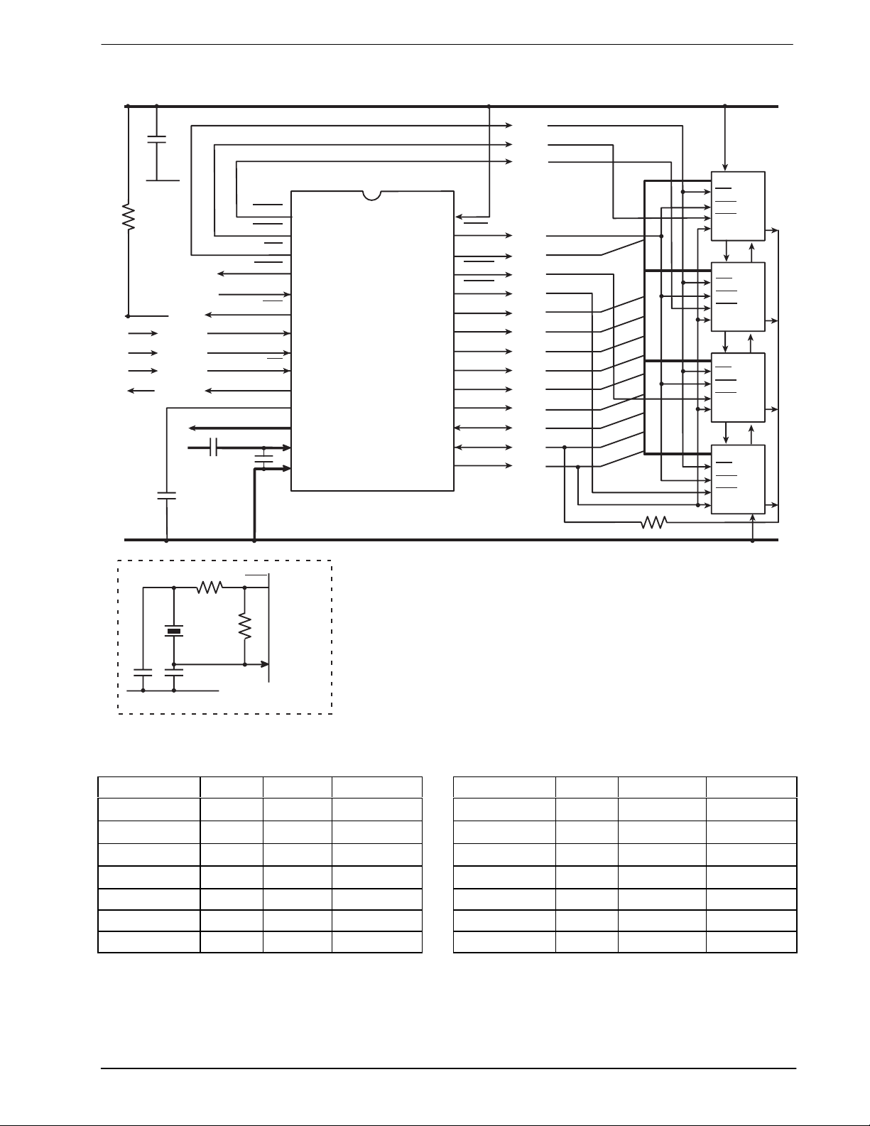
The MX802 Data/Voice Storage and Retrieval (DVSR) Codec contains a Continuously Variable Slope Delta
Modulation (CVSD) encoder and decoder as well as control and timing circuitry for up to 4Mbits of external
DRAM. As a member of the DBS800 series, it also contains interface and control logic for the “C-BUS” serial
interface.
When used with external DRAM, theMX802 had four primary functions: Speech Storage, Speech layback,
Data Storage, and Data Retrieval. The Speech Storage and Playback may be performed concurrently with
data storage or retrieval.
On-chip the Delta Codec is supported by input and output analog switched-capacitor filters and audio output
switching circuitry. The DRAM control and timing circuitry provides all the necessary address, control, and
refresh signals to interface to external DRAM.
The MX802 may also be used without DRAM (as a “stand alone” CVSD Codec), in which case direct access
is provided to the CVSD Codec digital data and clock signals. All signals are controlled by “C-BUS”
commands from the system microcontroller.
The MX802 may be used with a 5.0V power supply and is available in the following packages:
24-pin PLCC (MX802LH), 28-pin PLCC (MX802LH8), and 28-pin PDIP (MX802P).
1998 MX-COM, Inc. www.mxcom.com Tel: 800 638 5577 336 744 5050 Fax: 336 744 5054 Doc. # 20480033.008
4800 Bethania Station Road, Winston-Salem, NC 27105-1201 USA All trademarks and service marks are held by their respective companies.
Page 2

DVSR CODEC 2 MX802
Contents
Section Page
1 Block Diagram................................................................................................................3
2 Signal List.......................................................................................................................4
3 External Components....................................................................................................6
4 General Description.......................................................................................................7
4.1 Controlling Protocol ............................................................................................................. 8
4.1.1 Address/Commands...............................................................................................................8
4.1.2 Operation with DRAM.............................................................................................................8
4.1.3 Speech...................................................................................................................................9
4.1.4 Data Handling.......................................................................................................................10
4.2 Write to Control Register ................................................................................................... 12
4.2.1 General Reset......................................................................................................................12
4.2.2 Direct Access .......................................................................................................................12
4.2.3 Play Counter.........................................................................................................................12
4.2.4 DRAM Control......................................................................................................................12
4.2.5 Codec Powersave................................................................................................................12
4.2.6 Command Interrupt Enable.................................................................................................. 12
4.2.7 Store and Play Speech Synchronization..............................................................................12
4.2.8 Decoder and Encoder Control..............................................................................................12
4.3 Encoder and Decoder Control : Analog Input and Output Control..................................... 14
4.3.1 Time Compression of Speech..............................................................................................15
4.4 Read Status Register ........................................................................................................ 15
4.4.1 Interrupts..............................................................................................................................15
4.4.2 Power Register.....................................................................................................................15
5 Application – Codec Performance .............................................................................17
6 Performance Specifications........................................................................................19
6.1 Electrical Specifications..................................................................................................... 19
6.1.1 Absolute Maximum Limits ....................................................................................................19
6.1.2 Operating Limits...................................................................................................................19
6.1.3 Operating Characteristics.....................................................................................................20
6.1.4 Timing...................................................................................................................................21
6.2 Packages........................................................................................................................... 23
MXCOM, Inc. reserves the right to change specifications at any time without notice.
1998 MX-COM, Inc. www.mxcom.com Tel: 800 638 5577 336 744 5050 Fax: 336 744 5054 Doc. # 20480033.008
4800 Bethania Station Road, Winston-Salem, NC 27105-1201 USA All trademarks and service marks are held by their respective companies.
Page 3
DVSR CODEC 3 MX802
1 Block Diagram
SERIAL
CLOCK
COMMAND
DATA
REPLY
DATA
C-BUS INTERFACE AND CONTROL LOGIC
DATA
READ
COUNTER
WE
CAS
DATA
WRITE
COUNTER
RAS1 RAS2
PLAY
COMMAND
BUFFER
SPEECH
PLAY
COUNTERS
DRAM CONTROL AND TIMING
RAS4
RAS3
STORE
COMMAND
BUFFER
SPEECH
STORE
COUNTERS
Figure 1: Block Diagram
IRQCS
CONTROL
REGISTER
ENCODER
DRAM ADDRESS LINES
DECODER
CLOCK
CLOCK
DIRECT ACCESS CLOCKS AND DATA
A2/DCKA3/ECKA4A5A6A7A8A9
STATUS
REGISTER
POWER
ASSESS
DRAM Data In/
A0/ENO
(ENCODER
OUT)
XTAL/
CLOCK
CLOCK
GENERATOR
ENCODE
CLOCK
DRAM Data Out/
XTAL
A1/DEI
(DECODER
IN)
AUDIO
IN
AUDIO
OUT
DECODE
CLOCK
IDLE
PATTERN
V
DD
V
BIAS
DEMODMOD
V
SS
1998 MX-COM, Inc. www.mxcom.com Tel: 800 638 5577 336 744 5050 Fax: 336 744 5054 Doc. # 20480033.008
4800 Bethania Station Road, Winston-Salem, NC 27105-1201 USA All trademarks and service marks are held by their respective companies.
Page 4
DVSR CODEC 4 MX802
2 Signal List
J/LH8 LH Signal Description
1
RAS2
Address Strobe input of the second 1Mbit DRAM chip (if used).
21
RAS1
Address Strobe input of the first DRAM chip.
32
4
Xtal
Enable Write
( EW ) The DRAM of Read/Write control pin.
This is the output of the 4.0MHz on –chip clock oscillator. External
components are required at the output when a Xtal is used. A Xtal
cannot be used with the 24-pin version.
5 3 Xtal/Clock This is the input to the on-chip clock oscillator inverter. A 4.0MHz Xtal
or externally derived clock should be connected here. See Figure 2.
This clock provides timing for on-chip elements, filters, etc. A Xtal
cannot be used with the 24-pin version. Various Xtal frequencies can
be used with this device. See Table 5 for Sampling Rate Variations.
64
IRQ
Request Interrupt The output of this pin indicates an interrupt condition
to the microcontroller by going to logic’0’. This ‘wire-or able’ output,
enabling the connection of up to 8 peripherals to 1 interrupt port on the
microcontroller. This pin is an open drain output. It therefore has a low
impedance pulldown to logic ‘0’ when active and a high impedance
when inactive. Conditions indicated by this function are Power Reading
Ready, Play Command Complete, and Store Command Complete.
7 5 Serial Clock This is the C-BUS serial clock input. This clock, produced by the
microcontroller, is used to transfer timing commands and data to and
from the DVSR Codec. See timing diagrams. Clock requirements vary
for different MX802 functions.
8 6 Command Data
This is the C-BUS serial data input from the microcontroller. Data is
loaded to this device in 8-bit bytes, MSB (bit 7) first, and LSB (bit 0) last,
synchronized to the Serial clock. See Timing diagrams.
97
CS
Select Chip : The C-BUS data transfer control function, this input is
provided by the microcontroller. Command Data transfer sequences are
initiated, completed, or aborted by the
Diagrams.
10 8 Reply Data
This is the C-BUS serial data output to the microcontroller. The
transmission of Reply Data bytes is synchronized to the Serial Data
Clock under the control of the Chip Select input. This 3-state output s
held at high impedance when not sending data to the microcontroller.
See Timing diagrams.
11 9 V
BIAS
This is the output of the on-chip analog circuitry bias system, held
internally at V
DD
C1. See Figure 2.
12 10 Audio Out This is the Analog signal out.
13 11 Audio In
This is the audio (speech) input. The signal to this pin must be AC
coupled by capacitor C4 and decoupled to V
optimum noise performance this input should be driven from a source
impedance of less than 100.
14 12 V
SS
15 13 Encoder Out
(ENO)
Negative Supply (GND)
DRAM Data In/A0/Direct Access -- This is connected to the DRAM data
input and address line A0. With no DRAM used, this output is available
in a Direct Access mode as the Delta Encoder digital data Output.
Direct Access control is achieved by Control Register byte 1, bit 7.
This pin should be connected to the Row
2 Strobe sRow Addres
1 Strobe sRow Addres This pin should be connected to the Row
CSsignal. See Timing
/2. This pin should be decoupled to VSS by capacitor
by HF capacitor C6. For
SS
1998 MX-COM, Inc. www.mxcom.com Tel: 800 638 5577 336 744 5050 Fax: 336 744 5054 Doc. # 20480033.008
4800 Bethania Station Road, Winston-Salem, NC 27105-1201 USA All trademarks and service marks are held by their respective companies.
Page 5
DVSR CODEC 5 MX802
J/LH8 LH Signal Description
16 14 Decoder In (DEI)
DRAM Data Out/A1/Direct Access --: This is connected to the DRAM
data output and address line A1. With no DRAM used, this pin is
available in a Direct Access mode as the Delta Decoder Clock input.
Direct Access control is achieved by Control Register byte 1, bit 6.
17 15 Decoder Clock
(DCK):
DRAM A2/Direct Access -- This is the DRAM address line A2. With no
DRAM employed, this pin is available in a Direct Access mode as the
Delta Decoder Clock Input. Direct Access control is achieved by Control
Register byte 1, bit 6.
18 16
Encoder Clock
(ECK)
DRAM A3/Direct Access: This is the DRAM address line A3. With no
DRAM employed, this pin is available in a Direct Access mode as the
Delta Encoder Clock Output. Direct Access control is achieved by
Control Register byte1, bit 6.
19 17 DRAM A4 DRAM address line 4.
20 18 DRAM A5 DRAM address line 5.
21 19 DRAM A6 DRAM address line 6.
22 20 DRAM A7 DRAM address line 7.
23 21 DRAM A8 DRAM address line 8.
24 RAS4
4 Strobe sRow Addres : This pin should be connected to the Row
Address Strobe input of the fourth 1Mbit DRAM chip (if used).
25
3RAS 3 Strobe sRow Addres : This pin should be connected to the Row
Address Strobe input of the third 1Mbit DRAM chip (if used).
26 22 DRAM A9
This is DRAM address line A9. This pin is not connected when a
256kbit DRAM is used. Note: To simplify PCB layout, the DRAM
address inputs A0-A8 may be connected in any physical order to the
DVSR Codec output pins A0-A8.
27 23
28 24 V
CAS Strobe AddressColumn : This is the DRAM Column Address Strobe
DD
pin. It should be connected to the
Positive supply. A single, stable +5 volt supply is required. Levels and
CASpins of all DRAM chips.
voltages within the DVSR Codec are dependent upon this supply.
Table 1: Signal List
1998 MX-COM, Inc. www.mxcom.com Tel: 800 638 5577 336 744 5050 Fax: 336 744 5054 Doc. # 20480033.008
4800 Bethania Station Road, Winston-Salem, NC 27105-1201 USA All trademarks and service marks are held by their respective companies.
Page 6
DVSR CODEC 6 MX802
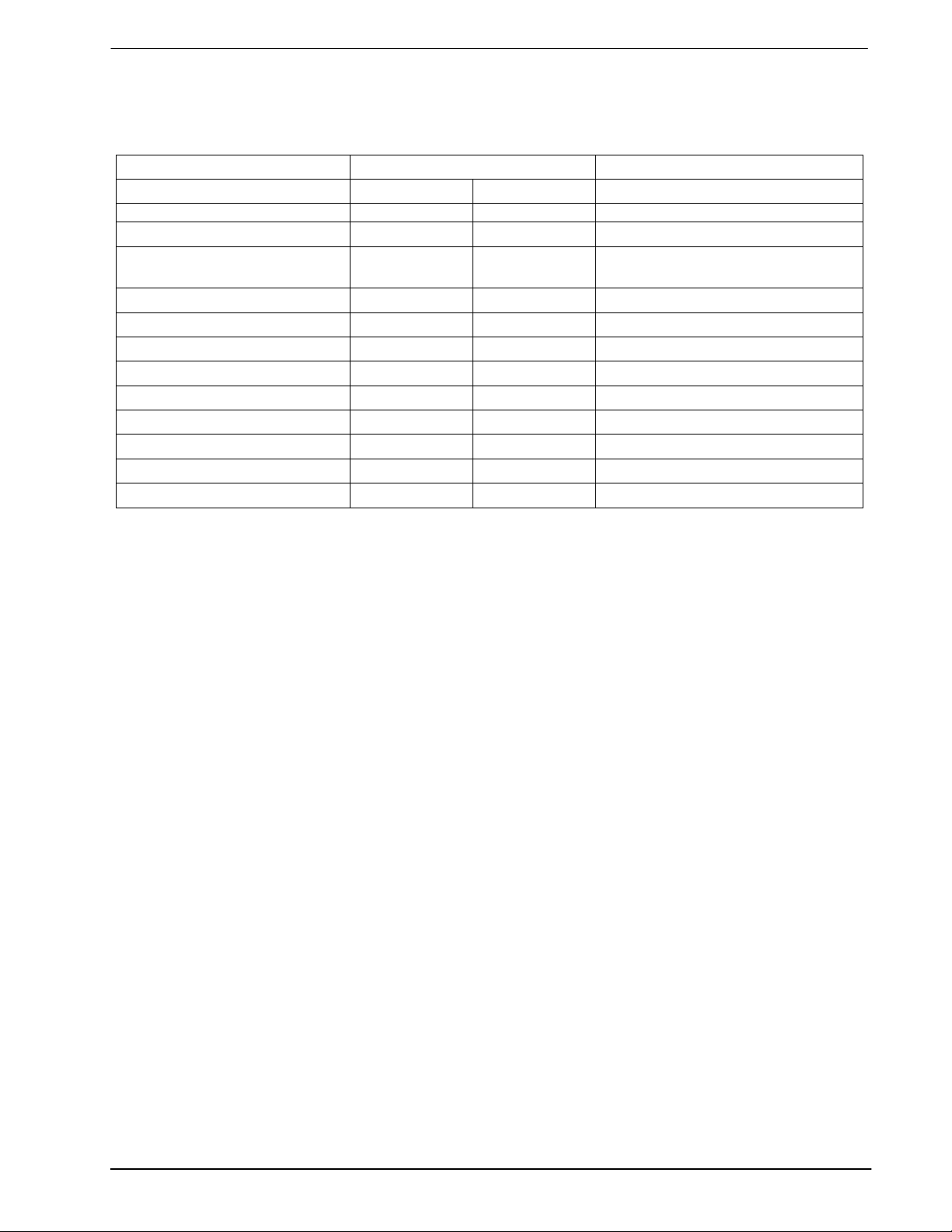
3 External Components
V
DD
C
V
SS
R
1
SEE INSET
C-BUS
INTERFACE
5
RAS2
RAS1
XT AL
XT AL/CLOCK
SERIAL CLOCK
COMMAND DAT A
REPLY DATA
AUDIO OUT
AUDIO IN
C
6
C
4
C
1
WE
IRQ
V
BIAS
V
CS
V
DD
1
*
2
3
4
*
5
6
7
MX802J
8
9
10
11
12
13
14
SS
V
SS
28
CAS
27
A9
26
RAS3
25
*
*
24
23
22
21
20
19
18
17
16
15
RAS4
A8
A7
A6
A5
A4
A3/ECK
A2/DCK
A1/DEI
A0/ENO
R
4
4X1Mbit
DRAM
A0 - A9
WE
CAS
RAS
D
A0 - A9
WE
CAS
RAS
D
A0 - A9
WE
CAS
RAS
D
A0 - A9
WE
CAS
RAS
D
Q
Q
Q
Q
INSET
C
3
X
1
C
2
XTAL
R
3
R
2
XTAL/CLOCK
V
SS
4
*
MX802J
5
Figure 2: Recommended External Components
Component Notes Value Tolerance Component Notes Value Tolerance
R1
R2
22.0k
1.0M
R3 1 ±10% C6
R4
1.0k
±5% C4 1.0µF ±20%
±10% C5 1.0µF ±20%
.001F
±20%
±10%
C1 1.0µF ±10% X1 4.00MHz
C2 33.0pF ±20% X1 4.032MHz
C3 33.0pF ±20% X1 4.096MHz
Table 2: Recommended External Components
1998 MX-COM, Inc. www.mxcom.com Tel: 800 638 5577 336 744 5050 Fax: 336 744 5054 Doc. # 20480033.008
4800 Bethania Station Road, Winston-Salem, NC 27105-1201 USA All trademarks and service marks are held by their respective companies.
Page 7

DVSR CODEC 7 MX802
Recommended External Component Notes:
1. Xtal circuitry shown in inset is in accordance with the MX-COM Standard and DBS 800 Crystal
Application Note.
2. External Xtal circuitry is not applicable to the 24-pin/lead version of this device. Only an externally
derived clock input can be used.
3. Functions whose pins are marked with and asterisk (*) in Figure 2 are not available on the 24-pin/lead
versions of this device. Pin numbers illustrated are for 28-pin versions.
4. Table 5 details the actual encoder/decoder sample rates available using the Xtal frequencies
recommended above.
5. Resistor R1 is used as the DBS800 system common pull-up for the C-BUS Interrupt Request
The optimum value will depend on the circuitry connected to the
IRQ . Up to 8 peripherals may be
IRQ
line.
connected to this line.
6. Recommended DRAM parameters:
256kbit x 1 or 1Mbit x 1 Dynamic Random Access Memory with
"RAS before CAS" refresh mode.
Maximum Row address time = .200us.
Example DRAM types:
256kbit (262,144 bits)
Texas Instruments (TMS4256-20)
Hitachi (HM51256-15)
1Mbit (1,048,576 bits)
Texas Instruments (TMS4C1024-15)
Hitachi (HM511000-15)
7. Figure 2 shows connections to 4x1 Mbit sections of DRAM. If desired, to simplify PCB layout, the DRAM
inputs A0-A8 may be connected in any order to the MX802 DVSR Codec output pins A0-A8.
Connections to 256kbit DRAM are similar, but A9 I left unconnected.
8. When using the MX802 “stand alone” 9Direct Access), no DRAM sections should be connected.
4 General Description
The MX802 Data/Voice Storage and Retrieval (DVSR) Codec contains a Continuously Variable Slope Delta
Modulation (CVSD) encoder and decoder as well as control and timing circuitry for up to 4Mbits of external
DRAM. As a member of the DBS800 series, it also contains interface and control logic for the “C-BUS” serial
interface.
When used with external DRAM, theMX802 had four primary functions: Speech Storage, Speech layback,
Data Storage, and Data Retrieval. The Speech Storage and Playback may be performed concurrently with
data storage or retrieval.
Speech Storage:
Speech signals present at the Audio Input may be digitized by the CVSD encoder. The
resulting bit stream is stored in DRAM. This process also provides readings of the
speech signal power level. These readings are used by the system microcontroller for
pause reduction.
Speech Playback:
Digitized speech may be read from DRAM and converted back into analog from by the
CVSD decoder.
Data Storage:
Digital data derived via the C-BUS from the Modem or system data may be stored in
DRAM.
Data Playback:
Digital data may be read from DRAM and sent over the C-BUS to the system
microcontroller.
On-chip the Delta Codec is supported by input and output analog switched-capacitor filters and audio output
switching circuitry. The DRAM control and timing circuitry provides all the necessary address, control, and
refresh signals to interface to external DRAM.
The MX802 may also be used without DRAM (as a “stand alone” CVSD Codec), in which case direct access
is provided to the CVSD Codec digital data and clock signals. All signals are controlled by “C-BUS”
commands from the system microcontroller.
1998 MX-COM, Inc. www.mxcom.com Tel: 800 638 5577 336 744 5050 Fax: 336 744 5054 Doc. # 20480033.008
4800 Bethania Station Road, Winston-Salem, NC 27105-1201 USA All trademarks and service marks are held by their respective companies.
Page 8
DVSR CODEC 8 MX802
4.1 Controlling Protocol
Control of the functions of the MX802 DVSR Codec is by a group of Address/Commands (A/Cs) and
appended instructions of data to and from the system microcontroller (See Figure 4). The use and content of
these instructions is detailed in the following pages.
Command Assignment Address/Command (A/C) byte Data Bytes
Hex Binary
MSB LSB
General Reset 01 00000001
Write to Control Register 60 01100000 +2 byte instruction to Control
Register
Read Status Register 61 01100001 +1 byte reply from Status Register
Store ‘N’ pages. Start page ‘X’ 62 01100010 +2 bytes command – Immediate
Store ‘N’ pages. Start page ‘X’ 63 01100011 +2 bytes Command – Buffered
Play ‘N’ pages. Start page ‘X’ 64 01100100 +2 bytes Command – Immediate
Play ‘N’ pages. Start page ‘X’ 65 01100101 +2 bytes Command – Buffered
Write Data. Start page ‘P’ 66 01100110 +2 bytes ‘P’ + Write Data
Read Data. Start page ‘P’ 67 01100111 +2 bytes ‘P’ + Read Data
Write Data – continue 68 01101000 +Write Data
Read Data -- Continue 69 01101001 +Read Data
Table 3: C-BUS Address/Commands
4.1.1 Address/Commands
Instruction and data transactions to and from this device consist of an Address/Command (A/C) byte followed
by further instruction/data reply.
Control and configuration is by writing instructions form the microcontroller to the Control Register (60
Reporting of MX802 configurations is by reading the Status Register (61
).
H
).
H
4.1.2 Operation with DRAM
The MX802 can operate with up to 4Mbits of Dynamic Ram (DRAM). When used with DRAM, the MX802
performs four main functions under the control of the commands received over the C-BUS interface from the
microcontroller:
Stores Speech
The MX802 stores speech by digitally encoding the analog input signal and writing the
resulting digital data into the associated DRAM.
Plays Speech
The MX802 plays back stored speech by reading the digital data stored in the DRAM and
decoding it to provide and analog output signal.
Writes Data
Reads Data
The MX802 writes data sent ver the C-BUS from the microcontroller to DRAM.
The MX802 reads data from DRAM, sending it to the microcontroller over the C-BUS.
Data is directed to and from DRAM by the on-chip DRAM Controller.
1998 MX-COM, Inc. www.mxcom.com Tel: 800 638 5577 336 744 5050 Fax: 336 744 5054 Doc. # 20480033.008
4800 Bethania Station Road, Winston-Salem, NC 27105-1201 USA All trademarks and service marks are held by their respective companies.
Page 9

DVSR CODEC 9 MX802
4.1.3 Speech
The CVSD encoder and decoder sampling rates are independently set via the Control Register (See Table 4,
Table 5, and Table 6) to 16, 25, 32, 50, and 64kbps. This allows the user to choose between speech quality
and storage time while providing for time compression or expansion of the speech signals.
The DVSR Codec can handle from 256kbits to 4Mbits of DRAM, giving, in the case of the 32kbps sampling
rate, from 8 to 131 seconds of speech storage.
For speech storage purposes, the memory is divided into ‘pages’ of 1024 bits each, corresponding to 32ms at
32kbps sampling rate.
A 256 kbit DRAM contains 256 ‘pages’
A 1 Mbit DRAM contains 1024 ‘pages’
A 4 Mbit DRAM contains 4096 ‘pages’
When used without DRAM, the decoder sampling rate (8-64kbps) is determined by an external clock source
applied to the Decoder Clock pin.
4.1.3.1 Store and Play Speech Commands
Speech storage and playback may take place simultaneously. These commands are transmitted, via C-BUS,
to the MX802 in the following form:
STORE OR PLAY “N” (1024-bit) PAGES (of decoded speech data) STARTING AT PAGE “N”.
“N” can be any number between 0 and F (1-16 pages). “X” can be any number from 405 (4Mbit DRAM), as
shown below. Preceded by A/C, this command writes 16 bits (byte 1 or byte0) of data from the
microcontroller to the Store or Play command Buffer.
MSB
BYTE 1 BYTE2
LSB
151413121110987654321 0
N X
4.1.3.2 Speech Store Commands
4.1.3.2.1 62
STORE “N” PAGES – START PAGE “X” (immediate)
H
STORE “N” PAGES – START PAGE “X” (buffered)
63
H
The digitized speech from the CVSD encoder is stored in consecutive DRAM locations with the Speech Store
Counters sequencing through the DRAM addresses and counting the number of complete pages stored since
the start of the execution of the command.
As soon as the command has terminated, the following events take place:
1. The Store Command Complete bit in the Status Register (Table 7) is set.
2. An Interrupt Request (
) is sent, if enabled, to the microcontroller.
IRQ
3. The next speech storage command (if present) is immediately taken from the Store Command Buffer and
execution f the new command commences.
The
IRQ output is cleared by reading the Status Register:
4.1.3.2.2 61H READ STATUS REGISTER (Table 8)
To provide continuity of speech commands, both Store and Play Commands can be presented to the MX802
in one of two formats: immediate or buffered.
An immediate command will be started on completion of its loading, irrespective of the condition of the current
command.
A buffered command will begin after the completion of the current Store or Play command, unless Speech
Synchronization Bits (Control Register) are set.
Buffering of commands lets the DVSR Codec execute a series of commands without intervening gaps even
though the microcontroller may take several milliseconds to respond to each “Command Complete” Interrupt
Request.
In either case, the Store or Play Command Complete bit of the status register will be cleared.
1998 MX-COM, Inc. www.mxcom.com Tel: 800 638 5577 336 744 5050 Fax: 336 744 5054 Doc. # 20480033.008
4800 Bethania Station Road, Winston-Salem, NC 27105-1201 USA All trademarks and service marks are held by their respective companies.
Page 10

DVSR CODEC 10 MX802
4.1.3.3 Speech Playback
Speech playback is controlled by similar commands using the Speech Play counters and Play Command
Buffer:
4.1.3.3.1 64
PLAY “N” PAGES – START PAGE “X” (immediate)
H
PLAY “N” PAGES – START PAGE “X” (buffered)
65
H
As soon as the Play Command had completed, the “Play Command Complete” bit in the Status Register is
set, and an Interrupt Request is generated (if enabled).
If no “next” command is waiting in the Play Command Buffer when a speech play command finishes, a
continuous idle code (0101…0101) will be fed to the delta decoder.
Speech data is stored or recovered at the selected Encode or Decode sample rate (Table 5). Store or Play
Command Complete bits in the Status Register are cleared by the next Store or Play Command received from
the microcontroller, or by a General Reset (01
).
H
4.1.3.4 Store/Play Speech Synchronization (Table 6)
This capability is provided primarily for Time Domain Scrambling applications.
Speech Synchronization bits in the Control Register will produce the effects described below:
4.1.3.4.1 No Speech Sync Set:
Store and Play operations may take place completely independently.
4.1.3.4.2 Store after Play:
The next buffered store command will start on completion of a play command, while the next play command
sequence (if any) continues normally.
4.1.3.4.3 Play after Store:
The next buffered play command will start on completion of a store command, while the next store command
sequence (if any) continues normally.
These actions will continue while Speech Sync bits are set.
4.1.4 Data Handling
For the purpose of storing data sent via C-BUS from the microcontroller, the memory (DRAM) is divided into
“data pages” of 64 bits (8 bytes).
A 256kbit DRAM contains 4096 data pages.
A 1Mbit DRAM contains16384 data pages.
4Mbit DRAM contains 65536 data pages.
In accordance with C-BUS timing specifications, data is handled 8 bits (1 byte) at a time, although any
number of 8-bit blocks of data may be written to or read from the DRAM by a single command.
Data transfer is terminated by the Chip Select line going to a logic “1.”
4.1.4.1 C-BUS Data Transfer Limitations
For those commands which transfer data over the C-BUS between DRAM and the microcontroller (Write and
Read data), the C-BUS serial clock rate is limited to a maximum of:
125kHz if the VSR Codec is executing store and play commands.
250kHz if no speech Store or Play commands are active.
This limitation is due to the rate at which data goes into and out of the DRAM. All other commands and
replies (Control, Status, Reset) may use a maximum clock rate of 500kHz. See Figure 4.
4.1.4.2 Read Data
4.1.4.2.1 67
READ DATA -- START PAGE “P”
H
This command sets the Data Read Counter to “P,” page, and then reads data bytes from successive DRAM
locations, sending them to the microcontroller as Reply Data bytes. The Data Read Counter is incremented
by 1 for each bit read.
4.1.4.2.2 69
READ DATA CONTINUE
H
This command reads data bytes from successive DRAM locations determined by the Data Read Counter,
incrementing the counter by 1 for each bit read.
1998 MX-COM, Inc. www.mxcom.com Tel: 800 638 5577 336 744 5050 Fax: 336 744 5054 Doc. # 20480033.008
4800 Bethania Station Road, Winston-Salem, NC 27105-1201 USA All trademarks and service marks are held by their respective companies.
Page 11

DVSR CODEC 11 MX802
4.1.4.3 Write Data
4.1.4.3.1 66
WRITE DATA -- START PAGE “P”
H
This command sets the Data Write Counter to “P” page, and then writes data bytes to successive DRAM
locations, incrementing the Data Write Counter by 1 for each bit received via the C-BUS.
The Start Page, “P,” is indicated by loading a 2-byte word after the relevant Address/Command byte. This 16bit word allows data page addresses from 0 to 65535 (4Mbits DRAM).
4.1.4.3.2 68
WRITE DATA CONTINUE
H
This command writes data bytes to successive DRAM locations determined by the Data Write Counter,
incrementing the counter by 1 for each bit received over the C-BUS.
4.1.4.4 DRAM Speech Capacity
28-pin/lead versions of the MX802 may be used with a single 256kbit DRAM, or with up to 4 x 1Mbit of
DRAM. 24-pin/lead versions may only be used with a single 256kbit or 1Mbit DRAM. The different encode
and decode sampling clock rates available enable the user to set voice store and play times against
recovered speech quality. Table 4 gives information on storage capacity and Store/Playback times. Speech
data can be replayed at a different sample rate or in a reversed sequence (see Control Register for details).
DRAM Size Available bits Speech Pages Nominal Sample Rates (kbps)
16 25 32 50 64
256kbps 262144 256 16.0 10.0 8.0 5.0 4.0
1024kbps 1048576 1024 65.0 42.0 32.0 20.0 16.0
2Mbps 2097152 2048 131.0 84.0 65.0 42.0 32.0
3Mbps 3145738 3072 196.0 126.0 98.0 63.0 49.0
4Mbps 4194304 4096 262.0 168.0 131.0 84.0 65.5
Table 4: Sampling Clock Rates vs. Speech Storage/Playback Times
4.1.4.5 Encoder and Decoder Sampling Clocks
Encoder and decoder sampling clock rates are programmable via the Control Register. Table 5 shows the
range of sampling rates available for different Xtal/clock input frequencies and the counter ratios used to
produce them. Consideration should be given to the effect of different Xtal/clock frequencies upon the audio
frequency performance of the device.
Control Register
Byte 0, Bits
5 4 3 Dec.
Internal Counter
Division Ratio
Xtal Clock Frequency (MHz)
4.0 4.032 4.096
210Enc.
0 1 1 256 15.625 15.75 16.0
1 0 0 160 25.0 25.20 25.60
1 0 1 128 31.25 31.50 32.0
1 1 0 80 50.0 50.4 51.20
1 1 1 64 62.50 63.0 64.0
Table 5: Sampling Clock Rates Available
With respect to using a single Xtal/clock frequency for all DBS 800 devices in use, it should be noted that
a. A 4.032MHz Xtal/clock input will produce an accurate 1200-baud rate for the MX809 MSK Modem.
b. A 4.096MHz Xtal/clock input will generate exactly 16kbps, 32kbps and 64kbps Codec sampling clock
rates.
1998 MX-COM, Inc. www.mxcom.com Tel: 800 638 5577 336 744 5050 Fax: 336 744 5054 Doc. # 20480033.008
4800 Bethania Station Road, Winston-Salem, NC 27105-1201 USA All trademarks and service marks are held by their respective companies.
Page 12

DVSR CODEC 12 MX802
4.2 Write to Control Register
4.2.1 General Reset
Upon power-up the bits in the MX802 registers will be random (either 0 or 1). A General Reset Command
(01
) will be required to reset all devices on the C-BUS. It has the following effect on the MX802:
H
Control Register Set to 00
Status Register Set to 00
H
H
Clear Store and Play Command Buffers
4.2.2 Direct Access
External circuitry is allowed direct access to the Delta Codec data and sampling clocks, disabling the DRAM
timing circuitry. This permits the Delta Codec section of the MX802 to be used as a Delta Modulation voice
encoder and decoder.
Input audio is encoded and made available at the Encoder Out (ENO) pin. Speech data input to the Decoder
In (DEI) pin is decoded to give voice-band audio at the Audio Output.
Analog output switching remains under the control of the Control Register, but the decoder sampling clock
rate (8kbps to 64kbps) must be provided from an external source to the Decoder Clock (DCK) pin. To ensure
correct filter setting, Decoder Control bits (byte 0, bits 5, 4, 3) should be set to binary 1,1,1, where the
required rate approximates to a multiple of 25kbps.
Both the encoder internal sampling clock rate and input switching (Table 7) remain under the control of the
Control Register. The encoder internal sampling clock rate is available to external circuitry at the Encoder
Clock Out (ECK) pin.
4.2.3 Play Counter
The Play Counter direction may be set to run backward as well as forward. This can be used in a scrambling
system by replaying speech data in reverse order.
4.2.4 DRAM Control
A logic “1” will disable the DRAM Control Timing circuits and associated counters. The C-BUS Interface,
Clock Generator, Delta Codec and filters remain active. This bit should be set to logic “1” when the MX802 is
used in the Direct Access Mode.
Minimum DVSR Codec power consumption is achieved by setting both DRAM Control and Powersave bits to
logic “1.”
4.2.5 Codec Powersave
A logic “1” puts the Delta Codec and filters into Powersave Mode with V
maintained. The Clock
BIAS
Generator, C-BUS Interface, and DRAM Control and Timing remain active.
4.2.6 Command Interrupt Enable
A logic “1” set at the relevant bit will enable Interrupt Requests to the microcontroller when that command
operation is complete.
4.2.7 Store and Play Speech Synchronization
This is intended primarily for Time Domain Scrambling.
4.2.8 Decoder and Encoder Control
This individually sets decoder and encoder sampling clock rates, as well as the source of the audio output.
1998 MX-COM, Inc. www.mxcom.com Tel: 800 638 5577 336 744 5050 Fax: 336 744 5054 Doc. # 20480033.008
4800 Bethania Station Road, Winston-Salem, NC 27105-1201 USA All trademarks and service marks are held by their respective companies.
Page 13

DVSR CODEC 13 MX802
Setting Function
Byte 1 First Byte for Transmission
MSB
Bit 7
Bit 6 Direct Access
1
0
Bit 5 Play Counter
1
0
Bit 4 DRAM Control
1
0
Bit 3 Codec Powersave
1
0
Bit 2 Store Command Interrupt
1
0
Bit 1 Play Command Interrupt
1
0
Bit 0 Power Reading Interrupt
1
0
Not used – Set to ‘0’
Encoder Data out to A0/ENO
Encoder Clock to A3/ECK
Decoder Input from A1/DEI
Decoder Clock from A2/DCK
Normal DVSR Operation
Decrement
Increment
Disable DRAM
Enable DRAM
Powersave MX802
MX802 Enable
Enable Interrupt
Disable
Enable Interrupt
Disable
Enable Interrupt
Disable
Setting Function
Byte 0 Last Byte for Transmission
MSB
Bit 7 Bit 6
0
0
1
1
0
1
0
1
Store/Play Speech Sync.
No Sync
No Sync
Sync – Play after Store
Sync – Store after Play
Bit 5 Bit 4 Bit 3 Decoder Control
Idle (32kbps); Aud O/P from LPF
0
0
0
0
1
1
1
1
0
0
1
1
0
0
1
1
0
Idle (32kbps); Aud bypass
1
Idle (32kbps); Aud O/P at high Z
0
On-Sampling Rate 16kbps
1
On-Sampling Rate 25kbps
0
On-Sampling Rate 32kbps
1
On-Sampling Rate 50kbps
0
On-Sampling Rate 64kbps
1
Bit 2 Bit 1 Bit 0 Encoder Control
I/P at VBIAS; F/Idle (32kbps)
0
0
0
0
1
1
1
1
0
0
1
1
0
0
1
1
0
I/P at high Z; F/Idle (32kbps)
1
I/P at high Z; F/Idle (64kbps)
0
On-Sampling Rate 16kbps
1
On-Sampling Rate 25kbps
0
On-Sampling Rate 32kbps
1
On-Sampling Rate 50kbps
0
On-Sampling Rate 64kbps
1
Table 6: Control Register
1998 MX-COM, Inc. www.mxcom.com Tel: 800 638 5577 336 744 5050 Fax: 336 744 5054 Doc. # 20480033.008
4800 Bethania Station Road, Winston-Salem, NC 27105-1201 USA All trademarks and service marks are held by their respective companies.
Page 14

DVSR CODEC 14 MX802
4.3 Encoder and Decoder Control : Analog Input and Output Control
The Control Register, Byte 0: bits 0 to 5, are used together with the codec Powersave Bit (Byte 1: bit 3) to
control codec input/output conditions and sample rates. Figure 3 shows the codec functional situation.
AUDIO IN AUDIO OUT
INPUT
BIAS
200 k
(nom)
V
BIAS
MOD DEMOD
CVSD CODEC
AUDIO
BYP ASS
500 k
(nom)
V
BIAS
OUTPUT
BIAS
Figure 3: Analog Control (with reference to Figure 1)
Control Register Circuit Switches
Codec
Powersave
Decoder
Control
Audio
Bypass
Audio
Out
Output
Bias
OFF = Switch Open
ON = Switch ON
Bit
0
0
0
0
–
0
1
1
1
1
–
1
0
1
0
0
0
1
0
1
1
0
–
–
–
1
1
1
0
0
0
1
0
0
0
1
0
1
1
0
–
–
–
1
1
1
ON
OFF
OFF
–
OFF
OFF
ON
OFF
OFF
-
OFF
OFF
0
0
Encoder
Control
0
0
0
0
0
0
-
0
1
-
1
0
1
0
0
0
1
0
0
1
1
–
–
–
1
1
1
0
0
0
-
-
-
1
1
1
ON
OFF
OFF
ON
–
ON
OFF
OFF
OFF
OFF
–
OFF
Input
Bias
ON
OFF
OFF
OFF
–
OFF
ON
-
ON
OFF
OFF
OFF
OFF
–
OFF
ON
OFF
ON
ON
-
ON
Decoder idling fed with
“1010101…” pattern at
32kbps.
Decoder running at the
selected sampling rate.
Decoder circuits
powersaved.
Encoder running at 32kbps
but Encoder Data O/P forced
to idle pattern “01010…”
Encoder running at selected
sampling rate
Encoder circuits powersaved.
Note
1
1
2
Table 7: Analog Control (with reference to Figure 3)
Notes
1. If the Delta Codec is in the Direct Access mode, these sampling rates will be as provided by the externally
applied clock.
2. The input bias switch is operated by the Control Register Codec Powersave and Encoder Control bits to
provide a relatively low impedance path for V
to charge the input coupling capacitor whenever the
BIAS
codec is powersaved, or the encoder control bits are set to 0, so that input bias can be established
quickly prior to operation.
1998 MX-COM, Inc. www.mxcom.com Tel: 800 638 5577 336 744 5050 Fax: 336 744 5054 Doc. # 20480033.008
4800 Bethania Station Road, Winston-Salem, NC 27105-1201 USA All trademarks and service marks are held by their respective companies.
Page 15

DVSR CODEC 15 MX802
4.3.1 Time Compression of Speech
The 25kbps and 50kbps sampling rate options are provided for time compression and subsequent expansion
of speech signals.
For example, 1.0 seconds of speech stored at 50kbps may be transmitted in 0.8 seconds if played out at
64kbps, and finally restored to its original speed at the receiver by storing at 64kbps and playing out at
50kbps. A similar result (with a degraded SINAD) may be achieved by using 25kbps and 32kbps sampling
rates.
However, the speech frequencies are raised by time compression, and since the signal transmitted to air must
be band limited to 3400 Hz, the effective end-to-end bandwidth is 0.8 x 3400 Hz, which is approximately
2700 Hz.
4.4 Read Status Register
4.4.1 Interrupts
If enabled by the Control Register, an Interrupt Request (IRQ) is produced by the MX802 to report the
following actions:
Power Reading Ready
Store Command Complete
Play Command Complete
When an Interrupt is produced, the Status Register must be read to determine the source of the interrupt. This
action will clear the IRQ output.
The Store Command Complete bit (and an interrupt) is set on completion of a Store Command. This bit is
cleared by loading the next Store Command, or by a General Reset Command (01
The Play Command Complete bit (and an interrupt) is set on completion of a Play Command. This bit is
cleared by loading the next Play Command, or by a General Reset Command (01
The Power Reading Ready bit (and an interrupt) is set for every 1024 voice-data bits (1 page) from the
Encoder. This bit is cleared after reading the Status Register, or by a General Reset Command (01
4.4.2 Power Register
The power assessment element shown in Figure 1 assesses the input signal power for each encoded “page”
(every 1024 encoder output bits) by counting the number of “compand bits” (000 or 111 sequences in the
output bit stream) produced during that page (see Table 8) with typical encoder input power levels (dB).
At the end of each “page” the power reading ready bit of the status register is set, and an interrupt request is
generated (if enabled). The resulting count is converted to a 5-bit quasi-logarithmic form. The Power Register
reading is interpreted as follows:
00000 represents 0 compand bits
00001 represents 1 compand bit
11111 represents 512 compand bits, the maximum.
This power reading is placed in the status register to be read by the microcontroller. Figure 4 shows this
output, indicating the input power level.
).
H
).
H
).
H
1998 MX-COM, Inc. www.mxcom.com Tel: 800 638 5577 336 744 5050 Fax: 336 744 5054 Doc. # 20480033.008
4800 Bethania Station Road, Winston-Salem, NC 27105-1201 USA All trademarks and service marks are held by their respective companies.
Page 16

DVSR CODEC 16 MX802
Reading Function
MSB
Bit 7 Power Reading
1 Ready
Bit 6 Store Command
1 Complete
Bit 5 Play Command
1 Complete
Power Register
43210
0
0
0
0
0
0
0
0
1
0
0
0
1
0
0
0
0
1
0
0
0
1
0
0
1
1
0
0
1
1
0
0
0
0
1
0
0
0
1
0
1
0
1
0
1
0
1
0
0
1
1
0
0
1
1
0
1
1
1
0
1
1
1
0
0
0
0
1
0
0
0
1
1
0
0
1
1
0
0
1
0
1
0
1
0
1
0
1
1
1
0
1
1
1
0
1
0
0
1
1
0
0
1
1
1
0
1
1
1
0
1
1
0
1
1
1
0
1
1
1
1
1
1
1
1
1
1
1
Power Compand Bits/pg.
0
1
0
1
0
1
0
1
-39.0dB
0
1
-36.0
0
1
33.5
0
1
-30.0
0
1
-28.0
0
1
-25.0
0
1
-22.0
0
1
-19.0
0
1
-16.0
0
1
-10.0
0
1
-6.0
0
1
0db
0
1
0
1
2
3
4
5
6
7
8
10
12
14
16
18
20
22
24
32
40
48
56
64
72
80
88
128
192
256
320
384
448
512
Table 8: Status Register
30
20
10
5-Bit Power Reading
(Status Register - Bits 0 to 4)
0
-50
-40 -30 -20 -10
Input Frequency = 1.0 kHz
Sample Clock Rate = 32 kb/s
0 dB ref. = 308 mVrms
308 mVrms
0dB
Average Input Power Level (dB)
5
Figure 4: Typical Power Readings vs. Input Levels
1998 MX-COM, Inc. www.mxcom.com Tel: 800 638 5577 336 744 5050 Fax: 336 744 5054 Doc. # 20480033.008
4800 Bethania Station Road, Winston-Salem, NC 27105-1201 USA All trademarks and service marks are held by their respective companies.
Page 17

DVSR CODEC 17 MX802
5 Application – Codec Performance
+10
Gain (dB)
0
-10
-20
Input 0 dB Ref. = 308 mVrms
Input Level = -20 dB
SampleRates=16,32or63kbps
-30
-40
-50
-60
0.2
1
2
3
Figure 5: Typical Overall;; (Encoder + Decoder) Frequency Response
SINAD
(dB)
64 kbps
30
0dB
4
56
Frequency (kHz)
50 kbps
20
32 kbps
25 kbps
Input Frequency = 1.0 kHz
0 dB ref. = 308 mVrms
10
-30
-24 -18 -12
Input Level (dB)
-6
0
Figure 6: SINAD vs. Input Level at Different Sample Rates
1998 MX-COM, Inc. www.mxcom.com Tel: 800 638 5577 336 744 5050 Fax: 336 744 5054 Doc. # 20480033.008
4800 Bethania Station Road, Winston-Salem, NC 27105-1201 USA All trademarks and service marks are held by their respective companies.
Page 18

DVSR CODEC 18 MX802
SINAD
(dB)
30
600 Hz
+10
-10
-20
-30
-40
-50
0
20
1000 Hz
1500 Hz
Sample Rate = 32 kbps
0 dB ref. = 308 mVrms
10
-30
-24 -18 -12
Input Level (dB)
-6
0
Figure 7: SINAD vs. Input Level at Different Frequencies
Gain (dB)
Input 0 dB Ref. = 308 mVrms
Input Level = -20 dB
Sample Rates = 25 or 50 kbps
0dB
-60
0.2
1
2
3
Figure 8: Typical Overall (Encoder + Decoder ) Frequency Response
4
56
Frequency (kHz)
1998 MX-COM, Inc. www.mxcom.com Tel: 800 638 5577 336 744 5050 Fax: 336 744 5054 Doc. # 20480033.008
4800 Bethania Station Road, Winston-Salem, NC 27105-1201 USA All trademarks and service marks are held by their respective companies.
Page 19

DVSR CODEC 19 MX802
6 Performance Specifications
6.1 Electrical Specifications
6.1.1 Absolute Maximum Limits
Exceeding these maximum ratings can result in damage to the device.
General Notes Min. Typ. Max. Units
Supply (VDD-VSS) -0.3 7.0 V
Voltage on any pin to V
SS
Current
V
DD
V
SS
Any other pin -20 20 mA
J / LH / LH8 Packages
Total allowable Power dissipation
AMB
= 25C
at T
Derating above 25C
Operating Temperature -40 85
Storage Temperature -55 125
-0.3 VDD + 0.3 V
-30 30 mA
-30 30 mA
800 mW
10
mW/C above 25C
C
C
Table 9: Absolute Maximum Ratings
6.1.2 Operating Limits
Correct Operation of the device outside these limits is not implied.
Notes Min. Typ. Max. Units
Supply (VDD-VSS) 4.5 5.0 5.5 V
Operating Temperature -40 85
Xtal Frequency 4.0 MHz
Table 10: Operating Limits
C
1998 MX-COM, Inc. www.mxcom.com Tel: 800 638 5577 336 744 5050 Fax: 336 744 5054 Doc. # 20480033.008
4800 Bethania Station Road, Winston-Salem, NC 27105-1201 USA All trademarks and service marks are held by their respective companies.
Page 20

DVSR CODEC 20 MX802
6.1.3 Operating Characteristics
For the following conditions unless otherwise specified.
V
= 5.0V @ T
DD
Xtal/Clock Frequency = 4.0MHz, Audio Level 0dB ref. = 308mV
AMB
= 25C
RMS
Standard test signal f0 = 820Hz, Sample Rate 31.25kbps
Static Values Notes Min. Typ. Max. Units
Supply Current
IDD (enabled) 1 7.0 10.0 mA
IDD (powersave) 1 2.0 4.0 mA
Digital Interface
Input Logic Level
Logic 1 Input Level 2 3.5 V
Logic 0 Input Level 2 1.5 V
Output Logic Level
Output Logic 1 (IOH = 120A)
(IOH = -120A)
(IOH = -50A)
(IOH = 20A)
7 4.6 V
3 4.6 V
9 4.6 V
Output Logic 0
(IOL = 20A)
(IOL = 100A)
(IOL = 360A)
9 0.4 V
3 0.4 V
7, 8 0.4 V
Digital Input Current
VIN = Logic 1 or 0 2 1.0
Leakage Current into IRQ ‘OFF’ Output
44.0
A
A
Digital Input Capacitance 2 7.5 pF
Analog Impedance
Input Impedance 12 500
Output Impedance 1.5
K
k
Dynamic Values
Encoder
Analog signal Input Levels 5 -24.0 4.0 dB
Passband 10, 11 3400 Hz
Decoder
Analog Signal Output Levels 5 -24.0 4.0 dB
Passband 10, 11 300 3400 Hz
1998 MX-COM, Inc. www.mxcom.com Tel: 800 638 5577 336 744 5050 Fax: 336 744 5054 Doc. # 20480033.008
4800 Bethania Station Road, Winston-Salem, NC 27105-1201 USA All trademarks and service marks are held by their respective companies.
Page 21

DVSR CODEC 21 MX802
Static Values Notes Min. Typ. Max. Units
Encoder/Decoder (Full Codec)
Passband 10, 11 300 3400 Hz
Passband Gain 11 0 dB
Passband Ripple 11 -3.0 3.0 dB
Stopband 6.0 10 kHz
Stopband Attenuation 50.0 dB
SINAD Level 23.0 dB
Output Noise (Input Short Circuit) -50 dBp
Idle Channel Noise (Forced) -55 dBp
Xtal/Clock Frequency 6 4.0 MHz
Table 11: Operating Characteristics
Operating Characteristics Notes:
1. Does not include current drawn by any attached DRAM.
2. Serial Clock, Command Data, Chip Select, A1/DE1, and A2/DCK inputs
3.
4. When the
and A0 to A9 inputs.
,WE ,CAS
output is at V
IRQ
DD
.
5. The optimum range levels for a good Signal to Noise ratio.
6. Audio frequency response will vary with respect to Xtal/Clock frequency.
7. Reply Data output.
8.
IRQ output.
9. RAS output.
10. Passband is reduced to (typically) 2700Hz when a sample rate of 25kbps or 50kbps is used.
11. Measured with a –20dB input level to avoid a codec slope-overload.
12. For optimum noise performance this input should be driven from a source impedance of less that
100.
6.1.4 Timing
C-BUS Timing Min. Typ. Max. Units
ab c
t
CSE
t
CHS
t
HIZ
t
CSOFF
t
NXT
t
CK
Chip Select Low to First Serial Clock Rising Edge 2.0 4.0 8.0
Last Serial Clock Rising Edge to Chip Select High 4.0 4.0 8.0
Chip Select High to Reply Data High – Z 2.0
Chip Select High 2.0 4.0 8.0
Command Data Inter-Byte Time 4.0 8.0 16.0
Serial Clock Period 2.0 4.0 8.0
s
s
s
s
s
s
Direct Address Timing
t
CH
t
CL
t
SU
t
H
t
PCO
Decoder or Encoder Clock High 1.0
Decoder or Encoder Clock Low 1.0
Decoder Data Set Up Time 0.45
Decoder Data Hold Time 0.60
Encoder Clock High to Encoder Data Valid 0.75
s
s
s
s
s
tSU + tH = Data True Time
Table 12: Timing Information
1998 MX-COM, Inc. www.mxcom.com Tel: 800 638 5577 336 744 5050 Fax: 336 744 5054 Doc. # 20480033.008
4800 Bethania Station Road, Winston-Salem, NC 27105-1201 USA All trademarks and service marks are held by their respective companies.
Page 22

DVSR CODEC 22 MX802
Notes:
1. Minimum Timing Values
a. For all commands except “Read Data” and “Write Data” Commands.
b. For all “Read Data” and Write Data” commands when no “Speech Store” or “Speech Play” commands
are active.
c. For “Read Data” and “Write Data” commands when “Speech Store” or “Speech Play” commands are
active.
2. Depending on the command, 1 or 2 bytes of Command Data are transmitted to the peripheral MSB (bit7)
first and LSB (bit0) last. Reply data is read from the peripheral MSB (bit7) first and LSB (bit0) last.
3. To allow for different microcontroller serial interface formats, C-BUS compatible ICs are able to work with
either polarity Serial Clock pulses.
4. Data is clocked into and out of the peripheral on the rising Serial clock edge.
5. Loaded commands are acted upon at the end each command.
t
CHIP SELECT
t
CSE
SERIAL CLOCK
COMMAND DATA
76543210 76543210
MSB LSB
ADDRESS/COMMAND
REPL Y DA TA
Logic level is not important
BYTE
t
NXT
t
CK
FIRST DATA BYTE LAST DATA BYTE
76543210
MSB
FIRST REPLY DAT A BYTE LAST REPLY DATA BYTE
LSB
t
NXT
76543210
76543210
CSOFF
t
CSH
t
HIZ
Figure 9: C-BUS Timing Information
Figure 10: Codec Direct Access Timing
1998 MX-COM, Inc. www.mxcom.com Tel: 800 638 5577 336 744 5050 Fax: 336 744 5054 Doc. # 20480033.008
4800 Bethania Station Road, Winston-Salem, NC 27105-1201 USA All trademarks and service marks are held by their respective companies.
Page 23

DVSR CODEC 23 MX802
6.2 Packages
A
B
E1
PIN1
K
H
K1
C
E
T
L
J
J1
P
F
Figure 11: 28-pin CERDIP Mechanical Outline:
D
Order as part no. MX802J
PackageTolerances
DIM.
MIN.
A
1.440 (36.58)
B
0.510 (12.94)
C
0.165 (4.19)
E
0.640 (16.26)
E1
0.608 (15.43) 0.618 (15.70)
F
H
0.015 (0.38)
J
J1
K
0.050 (1.27)
K1
0.075 (1.91)
L
0.115 (2.92)
P
T
0.0090 (0.228)
NOTE: Alldimensions in inches (mm.)
Angles are in degrees
TYP. MAX.
1.460 (37.08)
0.530 (13.45)
0.230 (5.84)
0.715 (18.14)
1.300 (33.02)
0.050 (1.27)
0.018 (0.46)
0.055 (1.39)
0.080 (2.03)
0.080 (2.03)
0.171 (4.34)
0.100 (2.54)
0.0102 (0.259)
PackageTolerances
MAX.MIN.DIM.
B
pin 1
C
A
E
H
G
F
A
B
C
D
E
F
G
H
J
.450 (11.43)
.485 (12.32)
.045x45
.165 (4.20)
.026 (0.66)
.017 (0.43)
.410 (10.41)
.050 (1.27)
.070 (1.78)
.453 (11.51)
.495 (12.57)
typical
.180 (4.57)
.030 (0.76)
.021 (0.53)
.430 (10.92)
typical
.085 (2.16)
NOTE: Alldimensions in inches (mm.)
J
Figure 12: 28-pin PLCC Mechanical Outline:
Order as part no. MX802LH8
Angles are in degrees
1998 MX-COM, Inc. www.mxcom.com Tel: 800 638 5577 336 744 5050 Fax: 336 744 5054 Doc. # 20480033.008
4800 Bethania Station Road, Winston-Salem, NC 27105-1201 USA All trademarks and service marks are held by their respective companies.
Page 24

DVSR CODEC 24 MX802
E
B
A
D
W
PIN 1
P
G
F
Figure 13: 24-pin PLCC Mechanical Outline:
Y
W
C
K
J
T
H
PackageTolerances
A
0.380 (9.61)
B
0.380 (9.61)
0.128 (3.25)
C
0.417 (10.60)
D
0.417 (10.60)
E
F
G
H
J
0.047 (1.19)
K
0.049 (1.24)
P
0.006 (0.152)
T
30°
W
Y
NOTE: Alldimensions in inches (mm.)
Angles are in degrees
TYP. MAX.MIN.DIM.
0.409 (10.40)
0.409 (10.40)
0.146 (3.70)
0.435 (11.05)
0.435 (11.05)
0.250 (6.35)
0.250 (6.35)
0.023 (0.58)
0.022 (0.55)0.018 (0.45)
0.048 (1.22)
0.051 (1.30)
0.009 (0.22)
45°
6°
Order as part no. MX802LH
1998 MX-COM, Inc. www.mxcom.com Tel: 800 638 5577 336 744 5050 Fax: 336 744 5054 Doc. # 20480033.008
4800 Bethania Station Road, Winston-Salem, NC 27105-1201 USA All trademarks and service marks are held by their respective companies.
 Loading...