

Page 1
DATA BULLETIN
MX663
Call Progress Decoder
© 1999 MX-COM Inc. www.mxcom.com Tele: 800 638-5577 336 744-5050 Fax: 336 744-5054 Doc. # 20480165.003
4800 Bethania Station Road, Winston-Salem, NC 27105-1201 USA All trademarks and service marks are held by their respective companies.
PRELIMINARY INFORMATION
Features Applications
•
Worldwide Call Progress Tone Decoding:
Single and Dual Tones
Fax and Modem
Answer/Originate Tones
SIT (Special Information Tones)
Fast ‘US Busy’ Tone Detector
•
Adjustable Detection Threshold
•
Voice Detector
•
Low Power 3.3V/5.0V Operation
•
Call Progress Monitoring
Automatic Call Placement
•
Machine Dialing
•
Fax Tone Detection for Line Switching
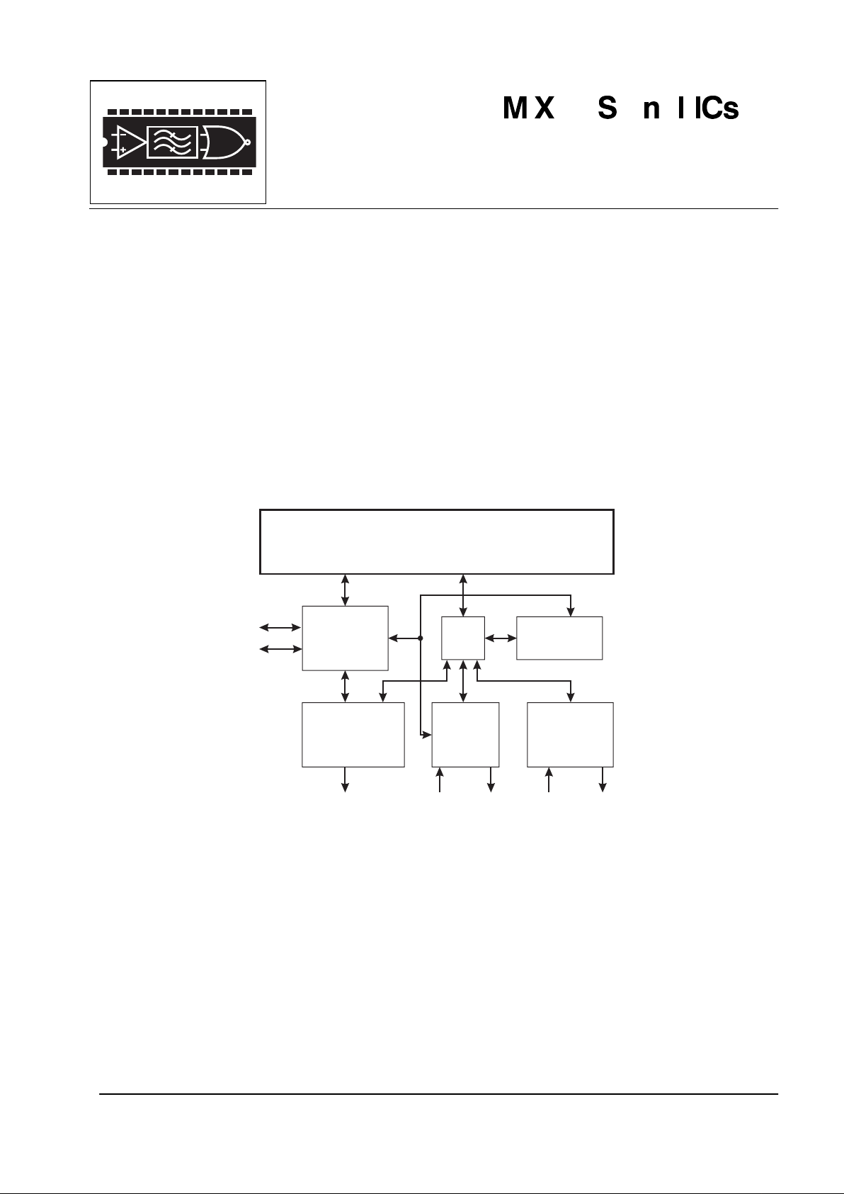
MX663
CALL PROGRESS DECODER
LINE INTERFACE
DTMF
KEYBOARD
AND DISPLAY
DRIVER
AUDIO
PROCESSING
RINGING CURRENT
GENERATOR/
LINE REVERSAL
DETECTOR
DETECTOR AND
µC
CODEC
The MX663 decodes the standard audible tone signals provided by telecom systems worldwide to indicate
Dial, Ringing, Busy, Unobtainable and other stages of a call attempt. It provides the key features needed for
intelligent, full-function, call progress monitoring by applications involving machine dialing or automatic call
placement. The MX663 also incorporates the following features:
•
Single and dual tone decoding for better cross-system Call Progress monitoring.
•
"US Busy" tone detector, saving time needed for "cadence verification" under Busy and Unobtainable
conditions. This incorporates a separate 620Hz detector for improved response.
•
A detector to indicate speech and non-call progress signals; this reduces voice falsing of call progress
tones and adds Voice-Answer detection as a "connected" prompt.
•
A fax and modem tone decoder.
•
A separate, adjustable threshold, signal-level detector which reduces noise falsing.
The MX663 uses digital signal processing techniques to provide these advantages. It is a low cost, low power
product with superior performance. The MX663 may be used with a 3.0 to 5.5 volt supply and is available in
the following packages: 16-pin SOIC (MX663DW) or 16-pin PDIP (MX663P).
Page 2

Call Progress Decoder 2 MX663 Preliminary Information
© 1999 MX-COM Inc. www.mxcom.com Tele: 800 638-5577 336 744-5050 Fax: 336 744-5054 Doc. # 20480165.003
4800 Bethania Station Road, Winston-Salem, NC 27105-1201 USA All trademarks and service marks are held by their respective companies.
CONTENTS
Section Page
1. Block Diagram................................................................................................................3
2. Signal List.......................................................................................................................4
3. External Components....................................................................................................5
4. General Description.......................................................................................................6
4.1 Overall Function Description ............................................................................................... 6
4.2 Glossary .............................................................................................................................. 6
4.3 Block Diagram Description (Reference Figure 1)................................................................ 6
4.3.1 SIGIN......................................................................................................................................6
4.3.2 Call Progress Detector: Signal Analyzer ................................................................................7
4.3.3 620Hz Detector ......................................................................................................................7
4.3.4 Control and Output Logic ......................................................................................................7
4.3.5 Level Detector and OPAMP ...................................................................................................7
4.3.6 Xtal/Clock Oscillator ...............................................................................................................7
4.3.7 Decode Output Truth Table....................................................................................................8
5. Application .....................................................................................................................9
5.1 General................................................................................................................................ 9
5.2 Signal Category Reference ................................................................................................. 9
5.3 Typical Response.............................................................................................................. 10
6. Performance Specification..........................................................................................11
6.1 Electrical Performance ...................................................................................................... 11
6.1.1 Absolute Maximum Ratings.................................................................................................. 11
6.1.2 Operating Limits...................................................................................................................11
6.1.3 Operating Characteristics.....................................................................................................12
6.2 Timing................................................................................................................................ 13
6.3 Packaging.......................................................................................................................... 16
MX COM, Inc. reserves the right to change specifications at any time and without notice.
Page 3
Call Progress Decoder 3 MX663 Preliminary Information
© 1999 MX-COM Inc. www.mxcom.com Tele: 800 638-5577 336 744-5050 Fax: 336 744-5054 Doc. # 20480165.003
4800 Bethania Station Road, Winston-Salem, NC 27105-1201 USA All trademarks and service marks are held by their respective companies.
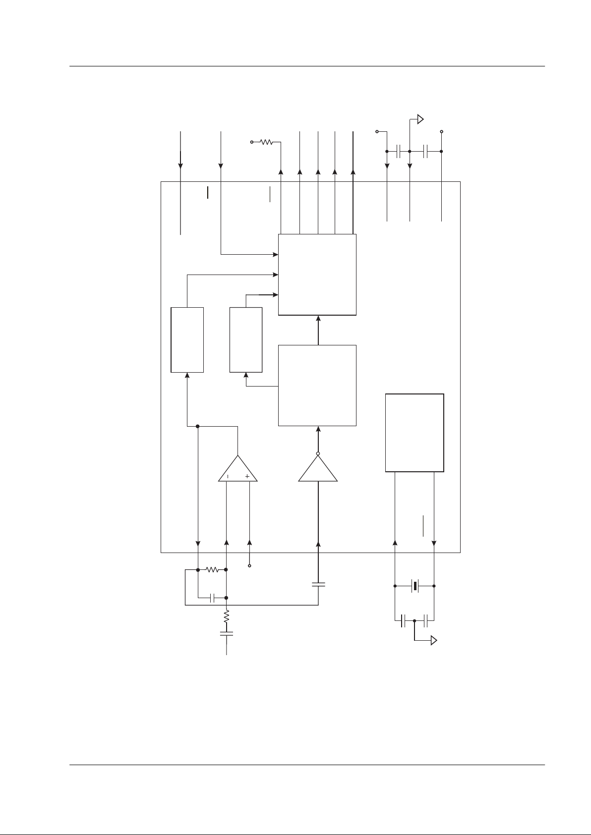
1. Block Diagram
V
BIAS
V
DD
LEVEL
DETECTOR
XTAL/CLOCK
XTAL
C1
C5
C2
X1
R2
R3
R1
CLOCK
OSCILLA TOR
AND
DIVIDERS
OPAMP
SIGIN
AMPOUT
IN-
IN+
ENABLE
C3
C4
CS
IRQ
D0
D2
D1
D3
620Hz
DETECTOR
SIGNAL
ANALYZER
CONTROL
AND
OUTPUT
LOGIC
MX663
SIGNAL
(Components shown for
unbalanced input)
V
SS
V
DD
V
BIAS
V
BIAS
V
DD
C7
C6
Figure 1: Block Diagram
Page 4
Call Progress Decoder 4 MX663 Preliminary Information
© 1999 MX-COM Inc. www.mxcom.com Tele: 800 638-5577 336 744-5050 Fax: 336 744-5054 Doc. # 20480165.003
4800 Bethania Station Road, Winston-Salem, NC 27105-1201 USA All trademarks and service marks are held by their respective companies.
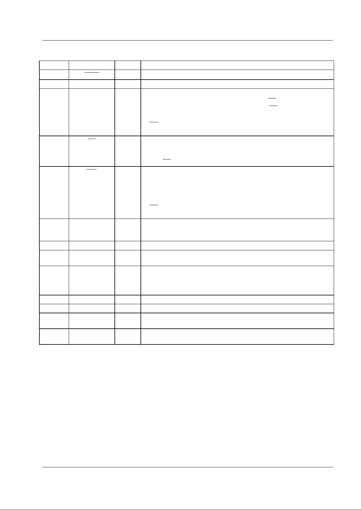
2. Signal List
Pin No. Signal Type Description
1
XTAL
output Inverted output of the on-chip oscillator.
2 XTAL/CLOCK input Input to the on-chip oscillator, for external Xtal circuit or clock.
3
4
5
6
D3
D2
D1
D0
output D3, D2, D1 and D0 is a 4-bit parallel data word output to the µC. The
transmission of data is under the control of the
CS
input. These 3-
state outputs are held at high impedance when
CS
is at "1". See
Figure 8
If
CS
is permanently at "0", D3, D2, D1 and D0 are permanently active.
See Figure 4 and Figure 7.
7
CS
input The chip select pin activates the Data Bus “D0: 3” when held low. A
µ
C can provide this input to allow the MX663 to reside on a shared
Data Bus. Data transfer sequences are initiated, completed or aborted
by the
CS
signal. See Figure 8
8
IRQ
output This output indicates an interrupt condition to the µC by going to a logic
"0". This is a "wire-ORable" output, enabling the connection of up to 8
peripherals to 1 interrupt port on the µC. This pin has a low impedance
pulldown to logic "0" when active and a high-impedance when inactive.
An external pullup resistor is required.
If
CS
is permanently at "0", the interrupt condition is a logic "0" pulse.
See Figure 4 and Figure 7.
9 ENABLE input A low level input selects the powersave mode, all circuits are reset and
disabled. D0 - D3 outputs become high impedance. A high level input
enables all circuits.
10 V
SS
Power Negative supply (ground).
11 SIGIN input Signal input. The signal to this pin should be ac coupled. The dc bias
of this pin is set internally.
12 V
BIAS
output Internally generated bias voltage, held at VDD/2 when the device is not
in powersave mode, it should be bypassed to V
SS
by a capacitor
mounted close to the device pins. In powersave mode this pin is pulled
towards V
SS
.
13 IN+ input Non-inverting input to the on-chip amplifier.
14 IN- input Inverting input to the on-chip amplifier.
15 AMPOUT output Output of the on-chip amplifier, this is internally connected to the input
of the Level Detector.
16 V
DD
Power The positive supply rail. Levels and voltages are dependent upon this
supply. This pin should be bypassed to V
SS
by a capacitor.
Table 1: Signal List
Page 5
Call Progress Decoder 5 MX663 Preliminary Information
© 1999 MX-COM Inc. www.mxcom.com Tele: 800 638-5577 336 744-5050 Fax: 336 744-5054 Doc. # 20480165.003
4800 Bethania Station Road, Winston-Salem, NC 27105-1201 USA All trademarks and service marks are held by their respective companies.
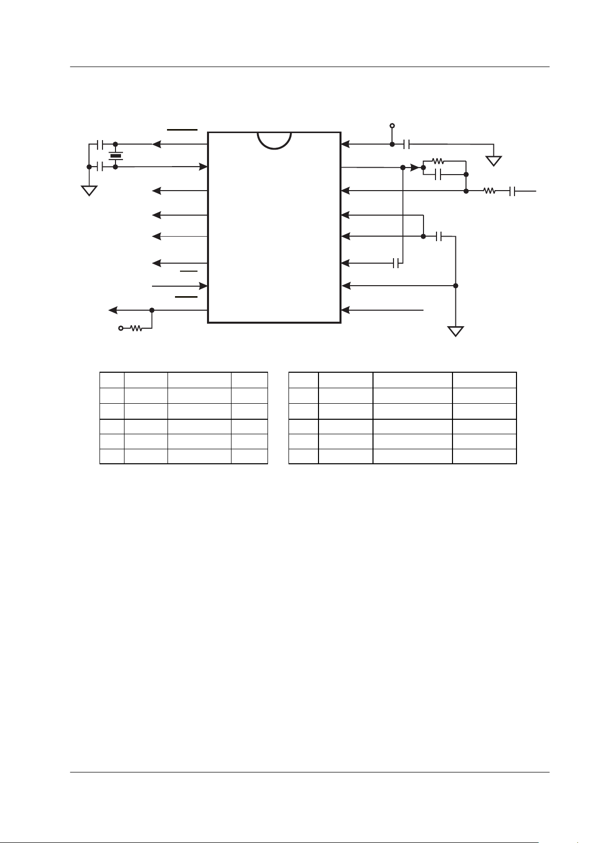
3. External Components
16
15
14
13
12
11
10
9
1
2
3
4
5
6
7
8
V
DD
AMPOUT
IN-
IN+
V
BIAS
SIGIN
ENABLE
R1
R2
C6
C3
C4
C5
C7
V
DD
V
SS
MX663
XTAL
XTAL
IRQ
CS
D3
D1
D2
D0
X1
R3
C1
C2
V
DD
Figure 2: Recommended External Components
R1 Note 3 100k
: ±10% C4 Note 3 0.1µF ±20%
R2 Note 3 510k: ±10% C5 Note 3 100pF ±20%
R3 20k: ±10% C6 1.0µF ±20%
C1 33pF ±20% C7 1µF ±20%
C2 33pF ±20%
C3 0.1µF ±20% X1 Note 1, 2 3.579545MHz ±100ppm
Table 2: Recommended External Components
Notes
1. A standard Color Burst Crystal Frequency is recommended.
2. For best results, a crystal oscillator design should drive the clock inverter input with signal levels of at
least 40% of V
DD
, peak to peak. Tuning fork crystals generally cannot meet this requirement. To
obtain crystal oscillator design assistance, consult your crystal manufacturer.
3. Reference section 4.3.5.
Page 6

Call Progress Decoder 6 MX663 Preliminary Information
© 1999 MX-COM Inc. www.mxcom.com Tele: 800 638-5577 336 744-5050 Fax: 336 744-5054 Doc. # 20480165.003
4800 Bethania Station Road, Winston-Salem, NC 27105-1201 USA All trademarks and service marks are held by their respective companies.
4. General Description
4.1 Overall Function Description
The MX663 consists of a Call Progress Tone Detector, a 620Hz Detector and a Level Detector.
The MX663 Call Progress Tone Detector uses different tone detection methods from those commonly found
with other products.
Many traditional devices use a bandpass filter followed by an energy detector. The filter is usually designed
to pass input signals with a frequency between about 300Hz and 700Hz, and the amplitudes of signals in this
range are then checked against a level threshold. Any signal of acceptable level in this frequency band is
classed as a Call Progress tone, including signals due to speech and noise. False outputs caused by speech
are a common feature with these products, and background noise may lead to a stuck "detect" output.
The MX663, by contrast, uses a stochastic signal processing technique based on analysis in both the
frequency and time domain, with signal amplitude forming a small part in the decision process. This analysis
includes checks on whether the signal has a "profile" which matches international standards for Call Progress
tones, or a profile more likely to match that of speech, noise or other non-call-progress signals. It also adds
checks on whether tones which include frequencies corresponding with the "US Busy" signals, Special
Information Tones and Fax/Modem Tones have been detected.
4.2 Glossary
Call Progress Tones: The single and dual frequency tones in the range 350Hz to 620Hz specified widely for
call progress signaling.
Call Progress Band: The nominal range 340Hz to 700Hz within which the MX663 will detect Call Progress
tones. The detection algorithm requires that the tones have the characteristics typical of Call Progress Tones.
620Hz Detection: The nominal range 590Hz to 650Hz. Single tones in this range, or dual tones having a
material frequency component within this range (e.g. 480 + 620Hz) will be detected.
Non Call Progress Signal: A signal falling within the nominal range (a) 190Hz to 895Hz, but NOT within the
Call Progress Band, or (b) within the nominal range 190Hz to 895Hz, but NOT meeting the DETECTION
REQUIREMENTS when the signal falls in the Call Progress Band.
Subject to the duration and other characteristics of such signals, the MX663 will usually interpret these as a
Non Call Progress Signal (e.g. speech or other signal activity).
Special Information Tone: The nominal frequencies 950Hz or 1400Hz or 1800Hz.
Fax/Modem Low Tone: The nominal frequency 1250Hz.
Fax/Modem High Tone: The nominal frequency 2150Hz.
Minimum Input Signal: The minimum signal level for the specified tone decoding performance. The lower
level at which absence of an input signal will be registered is not specified. However, a separate signal level
detector makes amplitude information available.
No Signal: A signal falling outside the nominal range 180Hz to 2280Hz or the absence of an input signal.
Either will be detected as a No Signal condition.
Nominal: Subject to dynamic tolerances within the signal analysis process. Absolute values are not material
or adverse to performance.
4.3 Block Diagram Description
(Reference Figure 1)
4.3.1 SIGIN
The input signal is amplified by a self-biased inverting amplifier. The dc bias of this input is internally set at.
Accordingly, the input signal should be capacitively coupled to SIGIN.
Page 7

Call Progress Decoder 7 MX663 Preliminary Information
© 1999 MX-COM Inc. www.mxcom.com Tele: 800 638-5577 336 744-5050 Fax: 336 744-5054 Doc. # 20480165.003
4800 Bethania Station Road, Winston-Salem, NC 27105-1201 USA All trademarks and service marks are held by their respective companies.
4.3.2 Call Progress Detector: Signal Analyzer
The analyzer samples the call progress signal at 9.322kHz. An external Anti-Alias Filter can be configured
using the on-chip opamp. The frequency range, quality and consistency of the input signal is analyzed by this
functional block. To be classified as a call progress signal the input signal frequencies should lie between
340Hz and 700Hz, the signal to noise ratio must be 16dB or greater and the signal must be consistent over a
period of at least 145ms. These decode criteria are continuously monitored and the assessment is updated
every 7ms. See section 4.3.5.
Because the analyzer time samples the input signal (SIGIN), signals above the operating band (2300Hz) can
alias, appear inband, and therefore be detected. Accordingly, applying signals above (2300Hz) should be
avoided. Such signals may be inadvertently generated by other sources such as digital clocks, switching
power supply, crosstalk, etc.
4.3.3 620Hz Detector
The detector is designed to aid detection of "US Busy" tone. The bandwidth of the 620Hz Detector is 60Hz
and the signal must be consistent over a period of at least 145ms for detection to occur. This assessment is
updated every 55ms.
4.3.4 Control and Output Logic
This block categorizes the nature of the signal into various decoded output states and controls the four
outputs. See the Truth Table in section 4.3.7.
4.3.5 Level Detector and OPAMP
The OPAMP is configured as an amplifier with external components R1, R2, C4 and C5. The level detector
operates by measuring the level of the amplified input signal and comparing it with a preset threshold which is
defined inside the MX663 as shown in the gain calculations below.
The detector output goes to the Control and Output Logic block. The data output is gated with the level
detector's output. The data output is valid only if the level detector output is true. The level detector output
can be forced true by connecting IN+ to V
BIAS
and IN- to VSS through a 100kΩ resistor. An interrupt is
produced if the output data changes state.
Gain Calculations:
1. Set gain so an input signal level is amplified above the threshold level of 250mV
P-P
.
Gain
mV
V
PP
IN
>
−
250
where VIN is the input signal level at C4 in mV
P-P.
In simplified form to assist with component value selection:
1. DC Gain = -R2/R1
2. C5 and R2 form a low-pass filter to attenuate out of band signals applied to SIGIN. The low pass filter’s
band edge is determined by the following: The recommended R2 and C5’s component values are
selected so than
f(-3dB) = 3120Hz .
fdB
RC
()
−=
⋅⋅ ⋅
3
1
225
π
3. C4 is a DC blocking capacitor, large enough to avoid affecting the AC gain in the frequency band of
interest.
4. The following formula defines the ac gain as a function of frequency, R1, R2 and C5 component values.
AC gain, Av(f)
()
Av f
R
RfRC
()
=
⋅+⋅⋅⋅⋅
1
212 25
2
π
4.3.6 Xtal/Clock Oscillator
If the on-chip Xtal oscillator is to be used, then external components X1, C1 and C2 are required. If an
external clock source is to be used, then it should be connected to the XTAL/CLOCK input pin and
the
XTAL
pin should be left unconnected.
Page 8

Call Progress Decoder 8 MX663 Preliminary Information
© 1999 MX-COM Inc. www.mxcom.com Tele: 800 638-5577 336 744-5050 Fax: 336 744-5054 Doc. # 20480165.003
4800 Bethania Station Road, Winston-Salem, NC 27105-1201 USA All trademarks and service marks are held by their respective companies.
4.3.7 Decode Output Truth Table
D3 D2 D1 D0 Conditions
0000No Signal
0001Call Progress Dual Tones:
Will detect 350+440, 400+450, 440+480 Hz tones
0010Non Call Progress Signal, e.g. Voice Activity
0011Call Progress Dual Tone including 620Hz Detection:
Will detect 480+620 Hz tones
0100Special Information Tone:
Will detect 950, 1400 and 1800 Hz tones
0101Call Progress Single Tone:
Will detect 400, 425, 440 and 450 Hz tones
0110Will detect a single tone lying outside the Call Progress
Band and within the Non Call Progress signal range
0111Call Progress Single Tone including 620Hz Detection:
Will detect 600 and 620 Hz tones
1000Fax/modem High Tone:
Will detect 2100 and 2200 Hz tones
1001Reserved for future use
1010Reserved for future use
1011Reserved for future use
1100Fax/modem Low Tone:
Will detect 1200 and 1300 Hz tones
1101Reserved for future use
1110Reserved for future use
1111Reserved for future use
Table 3: Decode Truth Table
Page 9

Call Progress Decoder 9 MX663 Preliminary Information
© 1999 MX-COM Inc. www.mxcom.com Tele: 800 638-5577 336 744-5050 Fax: 336 744-5054 Doc. # 20480165.003
4800 Bethania Station Road, Winston-Salem, NC 27105-1201 USA All trademarks and service marks are held by their respective companies.
5. Application
5.1 General
Apply a reset after power-up by taking the ENABLE pin low. This places the device in a powersave mode and
resets the internal circuits. It also places the data word output (D0-D3) in a high impedance state, regardless
of the level on the
CS
pin.
From this mode the device can be returned to normal operation without any additional settling time, when
using the component values recommended in Figure 2. The tone response times remain the same and are
given in section 6.1.
An interrupt is produced when the decode state is changed. This interrupt is reset by
CS
going to logic "0".
When
CS
is permanently at "0", the interrupt condition is a 5 µs logic "0" pulse on the
IRQ
pin. When CS is
set to logic "1", the data word output (D0-D3) goes into a high impedance state.
5.2 Signal Category Reference
Signal Category Sub-Category Output Code D
3:0
No Signal 0 0 0 0
Voice and
Non-Call Progress
Signal
Not Single Tone
Single Tone outside of CP band
0 X 1 0
0 0 1 0
0 1 1 0
Call Progress Signal
Dual Tone without 620Hz
Dual Tone with 620Hz
Single Tone not 620Hz
Single Tone 620Hz
0 X X 1
0 0 0 1
0 0 1 1
0 1 0 1
0 1 1 1
Special Information
Tone (SIT Tone)
N/A 0 1 0 0
FAX/MODEM Low
High
1 1 0 0
1 0 0 0
Unused Codes Reserved for future use 1 0 0 1, 1 0 1 0, 1 0 1 1, 1 1 0 1, 1 1 1 0, 1 1 1 1
Table 4: Signal Category
Page 10

Call Progress Decoder 10 MX663 Preliminary Information
© 1999 MX-COM Inc. www.mxcom.com Tele: 800 638-5577 336 744-5050 Fax: 336 744-5054 Doc. # 20480165.003
4800 Bethania Station Road, Winston-Salem, NC 27105-1201 USA All trademarks and service marks are held by their respective companies.
5.3 Typical Response
Figure 3: Typical Response Chart
Page 11

Call Progress Decoder 11 MX663 Preliminary Information
© 1999 MX-COM Inc. www.mxcom.com Tele: 800 638-5577 336 744-5050 Fax: 336 744-5054 Doc. # 20480165.003
4800 Bethania Station Road, Winston-Salem, NC 27105-1201 USA All trademarks and service marks are held by their respective companies.
6. Performance Specification
6.1 Electrical Performance
6.1.1 Absolute Maximum Ratings
Exceeding these maximum ratings can result in damage to the device.
General Min. Max. Units
Supply (VDD - VSS) -0.3 7.0 V
Voltage on any pin to V
SS
-0.3 V
DD
+ 0.3 V
Current
V
DD
-30 30 mA
V
SS
-30 30 mA
Any other pin -20 20 mA
P / DW Packages
Total Allowable Power Dissipation at T
AMB
= 25°C 800 mW
Derating above 25°C 13 mW/°C above 25°C
Storage Temperature -55 125 °C
Operating Temperature -40 85 °C
6.1.2 Operating Limits
Correct operation of the device outside these limits is not implied.
Notes Min. Max. Units
Supply (VDD - VSS)3.05.5V
Operating Temperature -40 85 °C
Xtal Frequency 3.57 3.59 MHz
Page 12

Call Progress Decoder 12 MX663 Preliminary Information
© 1999 MX-COM Inc. www.mxcom.com Tele: 800 638-5577 336 744-5050 Fax: 336 744-5054 Doc. # 20480165.003
4800 Bethania Station Road, Winston-Salem, NC 27105-1201 USA All trademarks and service marks are held by their respective companies.
6.1.3 Operating Characteristics
For the following conditions unless otherwise specified:
Xtal Frequency = 3.579545MHz (Color Burst Crystal)
V
DD
= 3.3V to 5.0V, T
AMB
= 25°C.
0dB = 775 mV
RMS
, S/N = 20dB, Noise Bandwidth = 5kHz Band Limited Gaussian
Notes Min. Typ. Max. Units
DC Parameters
I
DD
all powersaved 1, 2 30 µA
V
DD
= 3.3V 1 0.5 1 mA
V
DD
= 5.0V 1 1.0 2 mA
Logic Interface
Input Logic '1' 70% V
DD
Input Logic '0' 30% V
DD
Input Leakage Current Logic '1' or '0' -1.0 1.0 µA
Input Capacitance 7.5 pF
Output Logic '1' IOH = 120µA 90% V
DD
Output Logic '0' I
OL
= 360µA 10% V
DD
'Off' State Leakage Current 3 10.0 µA
AC Parameters
SIGIN Pin
Input Impedance 4 0.35
M
Ω
Minimum Input Signal Level -40.0 dB
Input Signal Dynamic Range 40.0 dB
Level Detector
Signal Level Detection Threshold measured at AMPOUT pin 5 -19.0 dB
OPAMP
Input Impedance 6 10.0
M
Ω
Voltage gain 500 V/V
Xtal/Clock Input
Pulse Width 'High' or 'Low' 7 40.0 ns
Input Impedance at 100Hz 10.0
M
Ω
Gain input = 1 mV
RMS
at 1kHz 20.0 dB
Notes:
1. Not including any current drawn from the device pins by external circuitry.
2. Enable input at V
SS
, CS input at VDD.
3.
IRQ
pin, D0 to D3 pins.
4. Small signal impedance over the frequency range 100Hz to 2300Hz and at 5.0V.
5. Input signal level is multiplied by the voltage gain (-R2/R1). The overall signal at AMPOUT should be
larger than 250mV
P-P
, for V
DD
= 5.0V. This threshold is proportional to VDD.
6. Open loop, small signal low frequency measurements.
7. Timing for an external input to the XTAL/CLOCK pin.
Page 13

Call Progress Decoder 13 MX663 Preliminary Information
© 1999 MX-COM Inc. www.mxcom.com Tele: 800 638-5577 336 744-5050 Fax: 336 744-5054 Doc. # 20480165.003
4800 Bethania Station Road, Winston-Salem, NC 27105-1201 USA All trademarks and service marks are held by their respective companies.
6.2 Timing
For the following conditions unless otherwise specified:
Xtal Frequency = 3.579545MHz, V
DD
= 3.3V to 5.0V, T
AMB
= 25°C.
Parameter Notes Min. Typ. Max. Units
t
RP
Call Progress Tone Response Time 1 145 ms
t
DRP
Call Progress Tone De-response Time 1 145 ms
t
NRP
Non Call Progress Signal Response Time 145 ms
t
NDRP
Non Call Progress Signal De-response Time 80 ms
t
I
Burst Length Ignored 1 70 ms
t
L
Burst Length Detected 1 145 ms
t
GI
Call Progress Tone Gap Length Ignored 1, 2, 3, 20 ms
t
GD
Call Progress Tone Gap Length Detected 1, 2 40 ms
t
NG
Non Call Progress Signal Gap Length Ignored 4 80 ms
t
DI
Data available to Interrupt pulse 430 µs
t
DE
"CS-Low " to Data Valid
0.2 µs
t
HIZ
"CS-High" to Output Tri-state
1.0 µs
t
IR
Interrupt Reset Time 0.2 µs
t
IP
Interrupt Low Pulse 4.0 5.0 6.0 µs
Notes:
1. Timing also applies to Special Information Tones and Fax/modem Tones.
2. Only applies to burst of the same frequency.
3. For Special Information Tones and Fax/Modem tones, t
GI
is 15ms maximum.
4. If the gap > 90ms, a NO Signal state will be detected.
D3
CS
"0"
"0"
IRQ
D0
D1
D2
SIGIN
ENABLE
t
DI
t
DE
t
HIZ
t
DI
t
IP
t
RP
t
RP
t
GD
t
GI
t
I
t
L
t
DRP
See Note 1
Tri-state
Tri-state
No Signal
Call Progres s
Single Tone
CPTone
620Hz
CPTone
620Hz
CPTone
620Hz
Note
1. D2 is '1' only when the Call Progress signal, or a Non Call Progress signal, is a single frequency tone.
Figure 4: Timing Diagram: Call Progress Tone(s)
Page 14

Call Progress Decoder 14 MX663 Preliminary Information
© 1999 MX-COM Inc. www.mxcom.com Tele: 800 638-5577 336 744-5050 Fax: 336 744-5054 Doc. # 20480165.003
4800 Bethania Station Road, Winston-Salem, NC 27105-1201 USA All trademarks and service marks are held by their respective companies.
D3
CS
"0"
"0"
"0"
IRQ
D0
D1
D2
SIGIN
ENABLE
t
DI
t
DE
t
IP
t
NRP
t
NG
t
I
t
L
t
NDRP
See Note 1
Tri-state
No Signal
Non Call
Progress Signal
Non Call
Progress Signal
Note:
1. D2 is '1' only when the Call Progress signal, or a Non Call Progress signal, is a single frequency tone.
Figure 5: Timing Diagram: Non Call Progress Signal
D3
CS
"0"
"0"
Tri-state Tri-state
"0"
"0"
IRQ
D0
D1
D2
SIGIN
ENABLE
t
DI
t
HIZ
t
DE
t
DI
t
IP
t
RP
t
RP
t
GD
t
GI
t
I
t
L
t
DRP
No Signal
Special
Information
Tone
Special
Information
Tone
Special
Information
Tone
Special
Information
Tone
Figure 6: Timing Diagram: Special Information Tones
Page 15

Call Progress Decoder 15 MX663 Preliminary Information
© 1999 MX-COM Inc. www.mxcom.com Tele: 800 638-5577 336 744-5050 Fax: 336 744-5054 Doc. # 20480165.003
4800 Bethania Station Road, Winston-Salem, NC 27105-1201 USA All trademarks and service marks are held by their respective companies.
D3
"0"
"0"
Tri-state Tri-state
"0"
CS
D0
D1
D2
SIGIN
ENABLE
t
DI
t
HIZ
t
DE
t
DI
t
IP
t
RP
t
RP
t
GD
t
GI
t
I
t
L
t
DRP
No Signal Fax/Modem
LowTone
Fax/Modem
High Tone
Fax/Modem
High Tone
Fax/Modem
High Tone
IRQ
Figure 7: Timing Diagram: Fax/Modem Tones
CS
IRQ
D0 to D3
SIGIN
ENABLE
Tri-State Tri-State
t
DI
t
IR
t
DE
t
HIZ
t
DI
t
RP
t
DRP
No Signal
Call Progress Signal
Figure 8: Bus Timing
Page 16

Call Progress Decoder 16 MX663 Preliminary Information
© 1999 MX-COM Inc. www.mxcom.com Tele: 800 638-5577 336 744-5050 Fax: 336 744-5054 Doc. # 20480165.003
4800 Bethania Station Road, Winston-Salem, NC 27105-1201 USA All trademarks and service marks are held by their respective companies.
6.3 Packaging
PIN 1
A
B
ALTERNATIVE
PIN
LOCATION
MARKING
X
P
J
Y
C
K
H
E
L
T
W
Z
NOTE: All dimensions in inches(mm.)
Angles are in degrees
PackageTolerances
A
B
C
E
H
TYP.
MAX.MIN.
DIM.
J
P
X
W
T
Y
K
L
0.105 (2.67)0.093 (2.36)
0.419 (10.64)
45°
7°
0° 10°
0.050 (1.27)
0.041 (1.04)
0.413 (10.49)
0.299 (7.59)
0.050 (1.27)
0.016 (0.41)
0.390 (9.90)
0.020 (0.51)0.003 (0.08)
0.009 (0.23) 0.0125 (0.32)
0.013 (0.33) 0.020 (0.51)
0.395 (10.03)
0.286 (7.26)
Z
5°
5°
Figure 9: 16-pin SOIC Mechanical Outline:
Order as part no. MX663DW
PackageTolerances
NOTE: All dimensions in inches(mm.)
Angles are in degrees
TYP. MAX.MIN.
A
B
C
E
E1
H
DIM.
J
J1
P
Y
T
K
L
0.200 (5.06)
0.262 (6.63)
0.390 (9.91).
7°
0.150 (3.81)
0.810 (20.57)
0.135 (3.43)
0.100 (2.54)
0.121 (3.07)
0.300 (7.62)
0.290 (7.37) 0.325 (8.26)
0.015 (0.38) 0.070 (1.77)
0.008 (0.20) 0.015 (0.38)
0.014 (0.35) 0.023 (0.58)
0.040 (1.02) 0.065 (1.65)
0.056 (1.42) 0.064 (1.63)
0.740 (18.80)
0.240 (6.10)
B
A
PIN 1
E
Y
E1
T
K
H
J1
J
C
P
L
Figure 10: 16-pin PDIP Mechanical Outline:
Order as part no. MX663P
 Loading...