

Page 1
COMMUNICATION SEMICONDUCTORS
查询CMX661供应商
CML Microcircuits
CMX661
PAIR GAIN DUAL
SPM DETECTOR
D/661/3 July 2002 Provisional Information
Features Applications
•• Two (12kHz/16kHz) SPM Detectors •• Pair-Gain Systems
•• Standard 3.579545MHz Xtal •• Out-of-Band Signalling Systems
•• Selectable Bandwidth Limits
•• Excellent Speech-Band Rejection
•• Low Power 3.0V to 5.0V Operation
•• Call Charge Applications in
PBX and PABX Line Cards
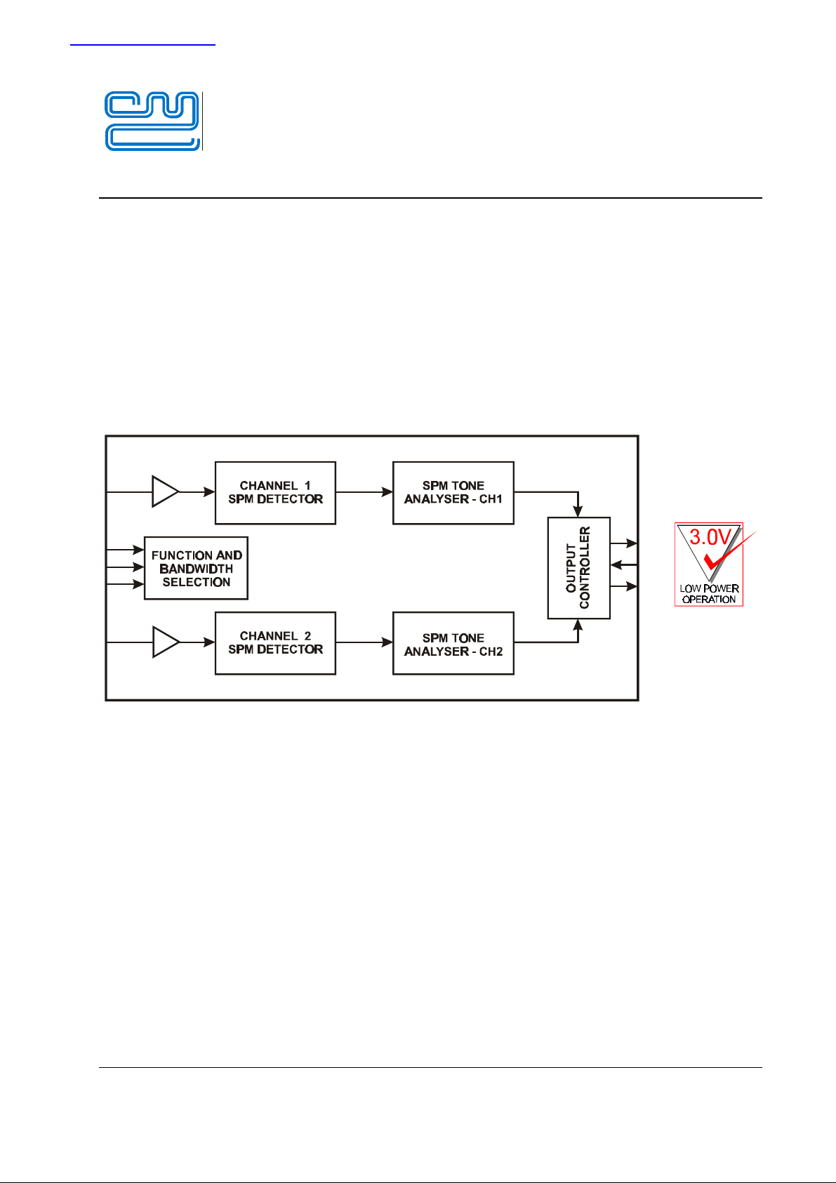
1.1 Brief Description
The CMX661 is a low power, Dual Subscriber Pulse Metering (SPM) Detector – two detectors on a single
chip – to indicate the presence on a telephone line of either 12kHz or 16kHz telephone call charge
frequencies. The detection frequency and bandwidth are common to both detectors and may be
externally selected. The detection sensitivity is set independently for each channel by external
components and the detector outputs can be set to a high impedance state for device multiplexing
requirements in PBX and PABX line card applications.
Flexibility of decode bandwidth settings allows the CMX661 to operate in systems where the SPM
generation is not necessarily perfectly accurate or stable. External hardwired selection of functionality
economises on the number of host µC I/O control lines required, whilst the rapid response and deresponse times of the CMX661 permit flexible tone length qualification by the host µC.
The CMX661 offers low (3.0V) operating voltage and power, consuming ≈750µA at 3V. It is available in
low-cost 16-pin plastic DIL and SOIC packages.
2002 CML Microsystems Plc
Page 2

Pair Gain Dual SPM Detector CMX661
CONTENTS
Section Page
1.0 Features and Applications..................................................................1
1.1 Brief Description..................................................................................1
1.2 Block Diagram .....................................................................................3
1.3 Signal List............................................................................................ 4
1.4 External Components..........................................................................6
1.5 General Description.............................................................................7
1.5.1 Description of Blocks .............................................................7
1.5.2 Operating States .....................................................................7
1.6 Application Notes................................................................................9
1.6.1 Signal Input Configurations................................................... 9
1.6.2 Crystal/Clock Distribution ......................................................9
1.6.3 Channel 1 and Channel 2 Output Format..............................9
1.6.4 Setting Level Sensitivity via External Components............10
1.6.5 Aliasing..................................................................................10
1.7 Performance Specification................................................................12
1.7.1 Electrical Performance..........................................................12
1.7.2 Packaging..............................................................................15
2002 CML Microsystems Plc 2 D/661/3
Page 3
Pair Gain Dual SPM Detector CMX661
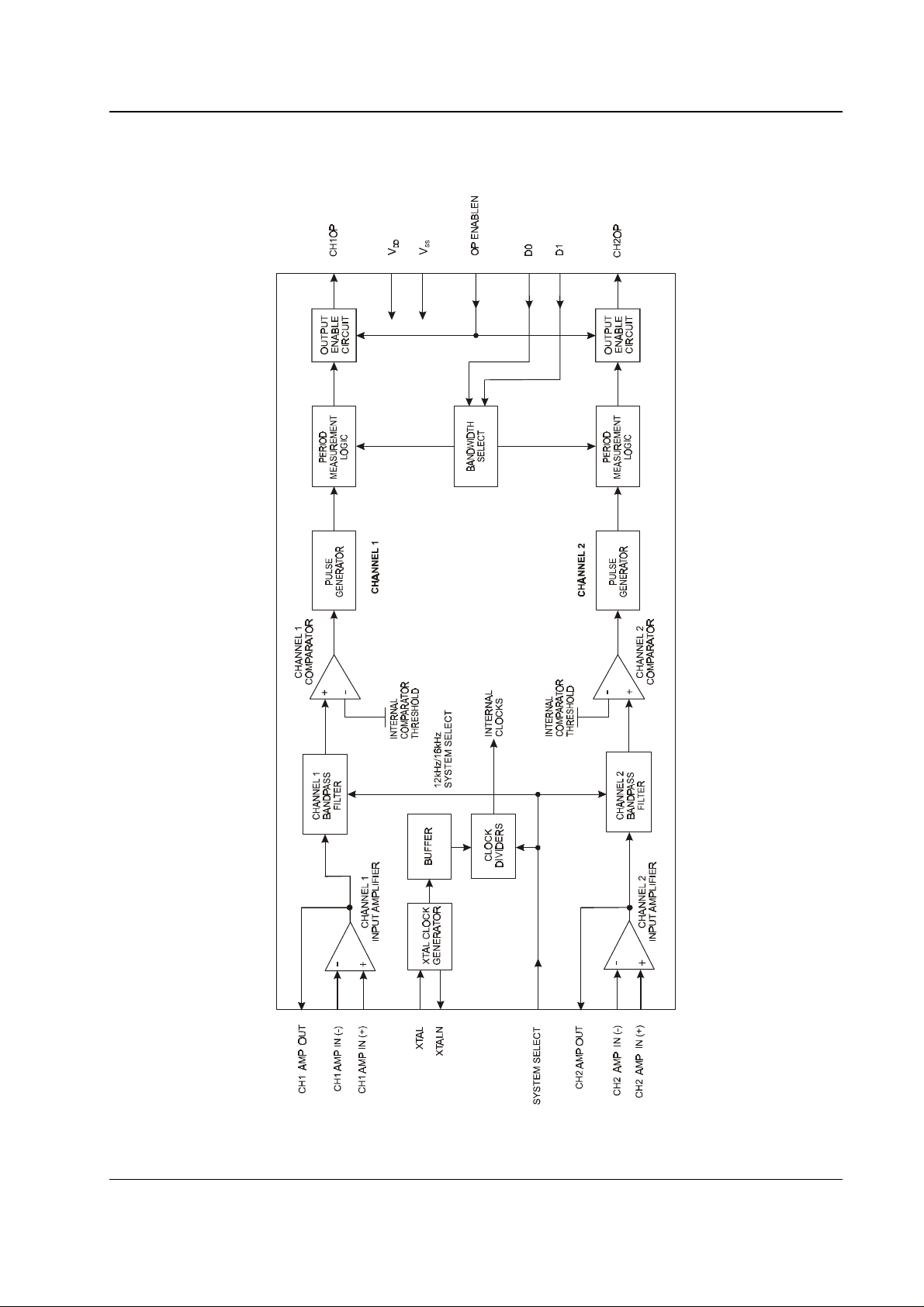
1.2 Block Diagram
Figure 1 Block Diagram
2002 CML Microsystems Plc 3 D/661/3
Page 4
Pair Gain Dual SPM Detector CMX661
1.3 Signal List
Package
D4
Pin No. Pin No. Name Type
1 1 XTAL I/P The input of the on-chip oscillator for use with a
2 2 XTALN O/P The inverted output of the on-chip oscillator.
3 3 CH2 OP O/P The digital output of the Channel 2 SPM
4 4 CH1 OP O/P The digital output of the Channel 1 SPM
Package
P3
Signal Description
3.579545MHz Xtal in conjunction with the
XTALN output; circuit components are on-chip.
detector, when enabled. Logic '0' (low) when
tone is detected.
detector, when enabled. Logic '0' (low) when
tone is detected.
5 5 CH1 AMP OUT O/P The output of the Channel 1 input amplifier.
See Figures 2 and 3.
6 6 CH1 AMP IN (-) I/P The negative input to the Channel 1 input
amplifier. See Figures 2 and 3.
7 7 CH1 AMP IN (+) I/P The positive input to the Channel 1 Input
amplifier. See Figures 2 and 3.
8 8 VSS POWER The negative supply rail (ground).
9 9 CH2 AMP IN (+) I/P The positive input to the Channel 2 input
amplifier. See Figures 2 and 3.
10 10 CH2 AMP IN (-) I/P The negative input to the Channel 2 input
amplifier. See Figures 2 and 3.
11 11 CH2 AMP OUT O/P The output of the Channel 2 input amplifier.
See Figures 2 and 3.
12 12 OP ENABLEN I/P For multi-chip output multiplexing; controls the
state of both Channel 1 and Channel 2 outputs.
When this input is placed high (logic ‘1’) both
outputs are set to a high impedance. When
placed at logic '0' (low) both outputs are
enabled.
13 13 D0 I/P
The LSB of the two bits which set the 'Will
Decode' bandwidth of the CMX661.
2002 CML Microsystems Plc 4 D/661/3
Page 5

Pair Gain Dual SPM Detector CMX661
Package
D4
Package
P3
Signal Description
Pin No. Pin No. Name Type
14 14 D1 I/P
The MSB of the two bits which set the 'Will
Decode' bandwidth of the CMX661.
15 15 SYSTEM
SELECT
I/P
Selects the system frequency. High (logic ‘1’) =
12kHz; Low (logic ‘0’) = 16kHz. This signal has
an internal pullup resistor, so if left unconnected
the CMX661 will detect 12kHz by default.
16 16 VDD POWER The positive supply rail. Critical levels and
voltages within the CMX661 are dependent
upon this supply. This pin should be decoupled
to VSS by a capacitor mounted close to the
device pins.
Notes: I/P = Input
O/P = Output
BI = Bidirectional
2002 CML Microsystems Plc 5 D/661/3
Page 6

Pair Gain Dual SPM Detector CMX661
1.4 External Components
Figure 2 Typical External Components
R1
R2
R3
R4
R5
R6
120kΩ
120kΩ
100kΩ
100kΩ
120kΩ
120kΩ
±1% R7
±1% R8
±1% R9
±1% R10
100kΩ
100kΩ
15kΩ
15kΩ
±1% C1 1.0µF ±20%
±1% C2 1.0µF ±20%
±1% C3 330pF ±5%
±1% C4 330pF ±5%
±1% C5 330pF ±5%
±1% X1 3.579545MHz C6 330pF ±5%
Input amplifier components R1, C3, R2, C4, R5, C5, R6 and C6 should be chosen to set the required
sensitivity of the CMX661 (see section 1.6.4). Typical values only are shown above. Note that when
calculating/selecting gain components, R3, R4, R7 and R8 should always be greater than or equal to
100kΩ. V
is not available from the CMX661 and so must be generated by an external voltage divider
BIAS
(R9 and R10) from VDD. Particular attention should be paid to decoupling VDD and keeping the power,
ground and signal lines free from unnecessary noise.
Telephone systems may have unusually high dc and ac voltages present on the line, as either differential
or common mode signals. If the CMX661 is part of a host system which does not have its own input
protection, then protection diodes must be added to both signal inputs (+ and ) so that the voltage on
any pin is limited to within VSS 0.3V and VDD + 0.3V. The breakdown voltage of capacitors and the
peak inverse voltage of diodes must be sufficient to withstand the sum of the dc and peak-peak ac
voltages applied.
2002 CML Microsystems Plc 6 D/661/3
Page 7

Pair Gain Dual SPM Detector CMX661
1.5 General Description
1.5.1 Description of Blocks
Crystal Oscillator and Clock Dividers
These circuits derive the internal logic clocks, decode frequencies and transmit frequencies by frequency
division of a reference frequency which is generated by the on-chip crystal oscillator. The only external
component required is a 3.579545MHz crystal, which should be connected across the XTAL and XTALN
pins. All other oscillator components are on-chip.
Input Operational Amplifiers
The input signals are applied to the CMX661 via these amplifiers, which use the external components
shown in Figure 2. The external gain setting components should be calculated by the method described
in section 1.6.4, using the values obtained from Figure 5.
SPM Tone Bandpass Filter
These are tone bandpass/audio reject filters automatically centred on the system frequency (12kHz or
16kHz) being detected. Their gain is constant so the internal device sensitivity is also constant.
Level Detection and Pulse Generator Circuits
The outputs from the bandpass filters are input to these circuits which perform the signal level
discrimination function for the CMX661. Signals which fulfil the system level requirements cause a
stream of digital pulses, one per 32 cycles of input signal, to be generated. These pulses are sent to the
period measurement circuitry.
Period Measurement Logic
This digital circuit block inputs the stream of pulses from the level detection circuits and measures their
repetition rate against a predetermined maximum and minimum. Because each pulse from the level
detect circuit occurs once per 32 cycles of input signal, this has the effect of averaging the input signal
period over this number of cycles. A valid SPM tone is recognised when 3 successive correctly spaced
pulses are received. This causes a signal to appear immediately at the relevant channel output
signifying receipt of a valid SPM signal. Depending upon the frequency, within the legal bandwidth,
received, the CMX661 should respond within 10-15ms (see section 1.7 and Figure 4).
Output Enable Circuits
These enable the output logic pins ‘Channel 1 Output’ and ‘Channel 2 Output’. These outputs can be
made high impedance by setting the OP ENABLEN pin high. When enabled, a high (logic ‘1’) indicates
the tone is absent, a low (logic ‘0’) indicates the tone is present.
1.5.2 Operating States
The CMX661 is a dual-channel SPM detector where both detectors are set to the same bandwidth and
system frequency (12kHz or 16kHz). The sensitivity of each detector is set via external components.
The decode bandwidths can be set to ±1.5%, ±3%, ±5% and ±7.5% of the nominal tone frequency by
means of the D0 and D1 logic inputs and the system frequency is set by the SYSTEM SELECT logic
input. Each decoder logic output has a very short response and deresponse time so that it forms an
‘envelope’ of the input tone. Host µC systems must decide whether the received signal fulfils the system
tone pulse length requirements. The outputs can be set to a high impedance state for device
multiplexing by use of the OP ENABLEN pin (logic '1' gives a high impedance state on the decoder
outputs, logic '0' gives a normal (logic) output on these pins).
The sensitivity of each channel is set by correct selection of external components around each channel
input amplifier. See section 1.6.4 and Figure 5 for a method of selecting amplifier gain and components
to meet a particular sensitivity requirement.
2002 CML Microsystems Plc 7 D/661/3
Page 8

Pair Gain Dual SPM Detector CMX661
Will Detect and Will Not Detect Bandwidths
There are four selectable bandwidths which are common to both channels. The ‘will detect’ bandwidth
can be programmed to ±1.5%, ±3%, ±5% or ±7.5%. The corresponding ‘will not detect’ band edges are
±4%, ±5.5%, ±7.5% and ±10%. Pins D0 and D1 program the bandwidth selection, shared by both
channels, as shown in Tables 4 and 5.
D0-D1
(both channels)
Lower
Will Not Detect
Lower
Will Detect
Upper
Will Detect
Upper
Will Not Detect
00 11.52kHz (-4.0%) 11.82kHz (-1.5%) 12.18kHz (+1.5%) 12.48kHz (+4.0%)
01 11.34kHz (-5.5%) 11.64kHz (-3.0%) 12.36kHz (+3.0%) 12.66kHz (+5.5%)
10 11.10kHz (-7.5%) 11.40kHz (-5.0%) 12.60kHz (+5.0%) 12.90kHz (+7.5%)
11 10.80kHz (-10.0%) 11.10kHz (-7.5%) 12.90kHz (+7.5%) 13.20kHz (+10.0%)
Table 4 Setting 12kHz Will Detect/Will Not Detect Bandwidths
D0-D1
(both channels)
Lower
Will Not Detect
Lower
Will Detect
Upper
Will Detect
Upper
Will Not Detect
00 15.36kHz (-4.0%) 15.76kHz (-1.5%) 16.24kHz (+1.5%) 16.64kHz (+4.0%)
01 15.12kHz (-5.5%) 15.52kHz (-3.0%) 16.48kHz (+3.0%) 16.88kHz (+5.5%)
10 14.80kHz (-7.5%) 15.20kHz (-5.0%) 16.80kHz (+5.0%) 17.20kHz (+7.5%)
11 14.40kHz (-10.0%) 14.80kHz (-7.5%) 17.20kHz (+7.5%) 17.60kHz (+10.0%)
Table 5 Setting 16kHz Will Detect/Will Not Detect Bandwidths
The CMX661 will always respond to valid inputs between the Lower ‘Will Detect’ and Upper ‘Will Detect’
frequencies inclusive. It will not respond to frequencies at or below the Lower ‘Will Not Detect’ or at or
above the Upper ‘Will Not Detect’.
System Select
The System Select pin selects the operating frequencies of the CMX661 (logic '1' = 12kHz, logic '0' =
16kHz).
2002 CML Microsystems Plc 8 D/661/3
Page 9

Pair Gain Dual SPM Detector CMX661
1.6 Application Notes
1.6.1 Signal Input Configurations
Figure 3 shows how the input amplifiers can be connected as differential mode or common mode
amplifiers, according to the application.
Figure 3 Example Input Configurations
External components are necessary to generate the bias voltage for the input op-amps. (The voltage
labelled V
capacitor to decouple the output.
1.6.2 Crystal/Clock Distribution
The CMX661 requires a 3.579545MHz crystal. With the exception of the crystal, all oscillator
components are incorporated on chip.
1.6.3 Channel 1 and Channel 2 Output Format
Figure 4 illustrates the output format, which is the same for both channels.
in Figure 3). This could be a potential divider consisting of two 15kΩ resistors and a 1.0µF
BIAS
Figure 4 Detector Output Format
2002 CML Microsystems Plc 9 D/661/3
Page 10

Pair Gain Dual SPM Detector CMX661
1.6.4 Setting Level Sensitivity via External Components
The sensitivities of the two channels are set by the correct selection of the components around the
Channel Input Amplifiers.
Input Gain Calculation: The input amplifiers, with their external circuitry, are available to set the
sensitivity of the CMX661 to conform to the user’s national level specification with regard to ‘Must’ and
‘Must-Not’ decode signal levels. With reference to the graph in Figure 5, the following steps will assist in
the determination of the required gain/attenuation.
Step 1
Draw two horizontal lines from the Y-axis {Signal Level dB(ref)}
The upper line will represent the required ‘Must’ decode level
The lower line will represent the required ‘Must-Not’ decode level.
Step 2
Mark the intersection of the upper horizontal line and the upper sloping line; drop a vertical line from this
point to the X-axis {Amplifier Gain (dB)}.
The point where the vertical line meets the X-axis will indicate the MINIMUM Input gain required for
reliable decoding of valid signals.
Step 3
Mark the intersection of the lower horizontal line and the lower sloping line; drop a vertical line from this
point to the X-axis.
The point where the vertical line meets the X-axis will indicate the MAXIMUM allowable Input amp gain.
Input signals at or below the ‘Must-Not’ decode level will not be detected as long as the amplifier gain is
no higher than this level.
Step 4
Refer to the gain components shown in Figure 2. The user should calculate and select external
components (R1/R3/C3, R2/R4/C4 and R5/R7/C5, R6/R8/C6) to provide amplifier gains within the limits
obtained in Steps 2 and 3.
Component tolerances should not move the gain figure outside these limits. Resistors R3, R4, R7 and
R8 should always be greater than or equal to 100kΩ. It is recommended that the designed gain is near
the centre of the calculated range.
Note that the device sensitivity is directly proportional to the applied power supply (VDD). The graph in
Figure 5 is for the calculation of input gain components for the CMX661 using a VDD of 5.0 (±0.1) volts.
Subtract 4.44dB from the amplifier gain for operation at 3.0V volts.
1.6.5 Aliasing
Due to the switched-capacitor filters employed in the CMX661, care should be taken to avoid any aliasing
effects by removing all frequencies above 579.390kHz (16kHz mode) or 434.543kHz (12kHz mode). This
can be achieved by adding bypass capacitors across R3, R4, R7 and R8, setting the -3dB breakpoint of
each resistor-capacitor combination such that there is sufficient attenuation at the alias frequency and
negligible effect at the desired SPM frequency.
2002 CML Microsystems Plc 10 D/661/3
Page 11

Pair Gain Dual SPM Detector CMX661
Figure 5 Input Gain Calculation Graph
2002 CML Microsystems Plc 11 D/661/3
Page 12

Pair Gain Dual SPM Detector CMX661
1.7 Performance Specification
1.7.1 Electrical Performance
1.7.1.1 Absolute Maximum Ratings
Exceeding these maximum ratings can result in damage to the device.
Min. Max. Units
Supply (VDD - VSS) -0.3 7.0 V
Voltage on any pin to VSS -0.3 V
Current into or out of VDD and V
pins -30 +30 mA
SS
Current into or out of any other pin -20 +20 mA
D4/P3 Package Min. Max. Units
Total Allowable Power Dissipation at Tamb = 25°C 800 mW
... Derating 13 mW/°C
Storage Temperature -55 +125 °C
Operating Temperature -40 +85 °C
1.7.1.2 Operating Limits
Correct operation of the device outside these limits is not implied.
Notes Min. Max. Units
Supply (VDD - VSS) 2.7 5.5 V
Operating Temperature -40 +85 °C
Xtal Frequency 3.558918 3.589368 MHz
+ 0.3 V
DD
2002 CML Microsystems Plc 12 D/661/3
Page 13

Pair Gain Dual SPM Detector CMX661
1.7.1.3 Operating Characteristics
For the following conditions unless otherwise specified:
Xtal Frequency = 3.579545MHz, Audio Level 0dB(ref) = 775Vrms. Noise Bandwidth = 50kHz,
V
Notes Min. Typ. Max. Units
DC Parameters
IDD 1 1.25 2.5 mA
IDD 2 0.75 1.5 mA
Logic Inputs
Input logic “1” level 80% VDD
Input logic “0” level 20% VDD
Input leakage current (Vin = 0 to VDD) 3 -5.0 +5.0 µA
Input capacitance 7.5 pF
Input current (Vin =0) 4 -15.0 µA
Channel Outputs
Output logic “1” level (1OH = 120µA) (Enabled) 90% VDD
Output logic “0” level (1OL = 360µA) (Enabled) 10% VDD
Off state leakage current (High Z output) -5.0 5.0 µA
Mode Change Time 5 500 ns
Response and De-Response time 6, 7, 8 15.0 ms
Input Amplifiers
Input impedance (at 100Hz) 10.0
Open Loop voltage gain (1mVrms I/P at 100Hz) 500 V/V
Common Mode range 10% 90% VDD
Input signal level 100% VDD
Output impedance (open loop) 6.0
Overall Performance
12kHz Detect Bandwidth 6, 9 11.82 12.18 kHz
12kHz Detect Bandwidth 6, 10 11.64 12.36 kHz
12kHz Detect Bandwidth 6, 11 11.40 12.60 kHz
12kHz Detect Bandwidth 6, 12 11.10 12.90 kHz
12kHz Not Detect Frequencies (below 12kHz) 6, 9 11.52 kHz
12kHz Not Detect Frequencies (below 12kHz) 6, 10 11.34 kHz
12kHz Not Detect Frequencies (below 12kHz) 6, 11 11.10 kHz
12kHz Not Detect Frequencies (below 12kHz) 6, 12 10.80 kHz
12kHz Not Detect Frequencies (above 12kHz) 6, 9 12.48 kHz
12kHz Not Detect Frequencies (above 12kHz) 6, 10 12.66 kHz
12kHz Not Detect Frequencies (above12kHz) 6, 11 12.90 kHz
12kHz Not Detect Frequencies (above12kHz) 6, 12 13.20 kHz
16kHz Detect Bandwidth 6, 9 15.76 16.24 kHz
16kHz Detect Bandwidth 6, 10 15.52 16.48 kHz
= 3.0V to 5.5V, Tamb = - 40°C to +85°C. System Setting = 12kHz or 16kHz.
DD
MΩ
kΩ
2002 CML Microsystems Plc 13 D/661/3
Page 14

Pair Gain Dual SPM Detector CMX661
1.7.1.3 Operating Characteristics (continued)
Notes Min. Typ. Max. Units
16kHz Detect Bandwidth 6, 11 15.20 16.80 kHz
16kHz Detect Bandwidth 6, 12 14.80 17.20 kHz
16kHz Not-Detect Frequencies (below 16kHz) 6, 9 15.36 kHz
16kHz Not-Detect Frequencies (below 16kHz) 6, 10 15.12 kHz
16kHz Not-Detect Frequencies (below 16kHz) 6, 11 14.80 kHz
16kHz Not Detect Frequencies (below 16kHz) 6, 12 14.40 kHz
16kHz Not-Detect Frequencies (above 16kHz) 6, 9 16.64 kHz
16kHz Not-Detect Frequencies (above 16kHz) 6, 10 16.88 kHz
16kHz Not-Detect Frequencies (above 16kHz) 6, 11 17.20 kHz
16kHz Not-Detect Frequencies (above 16kHz) 6, 12 17.60 kHz
Level Sensitivity
Level Sensitivity is set by external components
(see Figure 2)
Signal Quality Requirements for Correct
6, 7,
-25 -26.7 -28.5 dB
13
Operation (see Figure 2)
Signal to Noise Ratio (Amp input) 7, 14,
22.0 20.0 dB
15, 16
Signal to Voice Ratio (Amp input) 7, 14,
-36.0 -40.0 dB
15, 17
Signal to Voice Ratio (Amp output) 7, 14,
-25.0 -27.0 -29.0 dB
16, 17
Notes:
1. At 5.0V. Not including any current drawn from the pins by external circuitry.
2. At 3.0V. Not including any current drawn from the pins by external circuitry.
3. Logic pins with no internal pullup or pulldown resistors: OP ENABLEN, D0 and D1.
4. Logic pins with an internal pullup or pulldown resistor: SYSTEM SELECT.
5. Time taken to change between high impedance and operating modes, with a maximum
capacitive load of 30pF on an output.
6. With adherence to Signal to Voice and Signal to Noise specifications.
7. 12kHz and/or 16kHz system.
8. The time delay after device powerup, change of bandwidth setting or change in input signal
conditions, before the condition of the outputs can be guaranteed correct.
9. With ‘Will Detect’ bandwidth set to ±1.5%.
10. With ‘Will Detect’ bandwidth set to ±3.0%.
11. With ‘Will Detect’ bandwidth set to ±5.0%.
12. With ‘Will Detect’ bandwidth set to ±7.5%.
13. With input amplifier gain setting of 0dB via external components and measured at amplifier
output with VDD =5.0V. Signal sensitivity is proportional to VDD. Channels measured
individually.
14. For immunity to false responses and/or deresponses.
15. Common mode SPM and balanced voice signal.
16. With balanced SPM and voice signals. To avoid false deresponses due to saturation, the
peak to peak voice + noise level at the output of the input amplifier should be no greater than
the dynamic range of the device.
17. Maximum voice frequencies = 3.4kHz.
2002 CML Microsystems Plc 14 D/661/3
Page 15

Pair Gain Dual SPM Detector CMX661
1.7.2 Packaging
Figure 6 D4 Mechanical Outline: Order as part no. CMX661D4
Figure 7 P3 Mechanical Outline: Order as part no. CMX661P3
2002 CML Microsystems Plc 15 D/661/3
Page 16

Pair Gain Dual SPM Detector CMX661
Handling precautions: This product includes input protection, however, precautions should be taken to
prevent device damage from electro-static discharge. CML does not assume any responsibility for the
use of any circuitry described. No IPR or circuit patent licences are implied. CML reserves the right at
any time without notice to change the said circuitry and this product specification. CML has a policy of
testing every product shipped using calibrated test equipment to ensure compliance with this product
specification. Specific testing of all circuit parameters is not necessarily performed.
www.cmlmicro.com
Oval Park - Langford - Maldon - Essex
- CM9 6WG - England.
Tel: +44 (0)1621 875500
Fax: +44 (0)1621 875600
Sales: sales@cmlmicro.com
Technical Support:
techsupport@cmlmicro.com
4800 Bethania Station Road Winston-Salem - NC 27105 - USA.
Tel: +1 336 744 5050,
800 638 5577
Fax: +1 336 744 5054
Sales: us.sales@cmlmicro.com
Technical Support:
us.techsupport@cmlmicro.com
No 2 Kallang Pudding Road - 09 to
05/06 Mactech Industrial Building -
Singapore 349307
Tel: +65 7450426
Fax: +65 7452917
Sales: sg.sales@cmlmicro.com
Technical Support:
sg.techsupport@cmlmicro.com
 Loading...