

Page 1
DATA BULLETIN
© 1996 MX•COM, INC. Tele: 800 638 5577, 910 744 5050, Fax: 910 744 5054
Document #20480148.001 May 1996
Preliminary Information
• • International Special Information Tone Identification
• • Worldwide Tone Compatibility • • - 40°°C to 85°°C Operating Temp
• • Single and Dual Tone Detected • • Low Supply Current (0.3mA/0.5mA)
• • U.S. Busy-Detect Output • • Low Supply Voltage (3.3V/5.0V)
• • Voice-Detect Output • • Standard 3.58MHz Clock Input
• • Wide Dynamic Range > 40dBm • • Standard 8-pin DIP Package
DETECT2
DETECT3
DETECT1
SLICER
SIGIN
ENABLE
XTAL
SIGNAL
ANALYZER
CONTROL
LOGIC
CLOCK
V
SS
V
DD
CLOCK /
XTAL
AVAILABLE
PACKAGES
MX643P
8-pin PDIP
MX643DW
16-pin SOIC
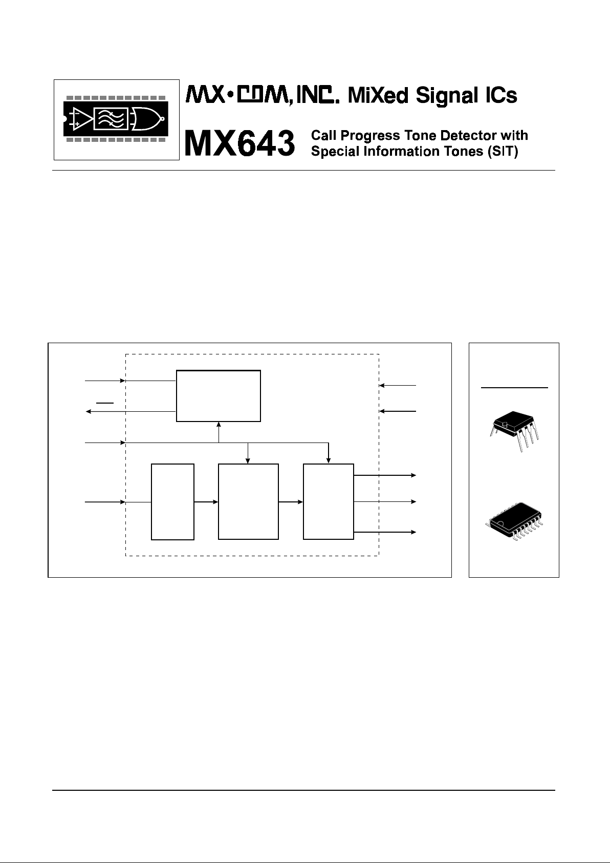
The MX643 is a low power, low cost device that uses signal processing techniques to detect audible tone signals
such as; Dial, Ring, Busy, Unobtainable, and other conditions found when placing a call throughout the world’s
telecom systems. The detection of these Call Progress stages is essential to the proper operation and application
of automatic calling products.
The MX643 offers identification of International Special Information Tones (SIT), reducing the time needed for
cadence verification under Obtainable conditions. In addition to the SIT feature, single and dual tone decoding
are added for better cross-system Call Progress monitoring. The MX643 offers these features in addition to the
same performance levels and features of the MX633 Call Progress Tone Detector such as; detection and
identification of U.S. Busy tones, thereby reducing the need to measure the tone cadence to identify U.S. Busy.
The decoding and indicating of speech, or other Non-Call Progress signals, thus reducing voice-falsing of Call
Progress tones and adding Voice-Answer as a connect prompt.
Available in the industry standard 8-pin DIP, the MX643 is also available in a 16-pin SOIC making it pin
compatible with the MX633DW (16-pin SOIC).
Page 2

Call Progress Tone Detector MX643 - Preliminary Information
© 1996 MX•COM, INC. Tele: 800 638 5577, 910 744 5050, Fax: 910 744 5054 Doc. #20480148.001
2
CONTENTS
Section Page
1. Block Diagram...............................................................................................................3
2. Signal List......................................................................................................................4
3. External Components...................................................................................................5
4. General Description......................................................................................................5
4.1 Glossary ............................................................................................................................ 5
4.2 Overall Function Description ............................................................................................. 6
5. Block Diagram Description..........................................................................................6
5.1 Decode Output Truth Table............................................................................................... 7
6. Performance Specification ..........................................................................................7
6.1 Electrical Performance...................................................................................................... 7
6.2 Packaging......................................................................................................................... 11
MX•COM, Inc. reserves the right to change specifications at any time and without notice.
Page 3
Call Progress Tone Detector MX643 - Preliminary Information
© 1996 MX•COM, INC. Tele: 800 638 5577, 910 744 5050, Fax: 910 744 5054 Doc. #20480148.001
3
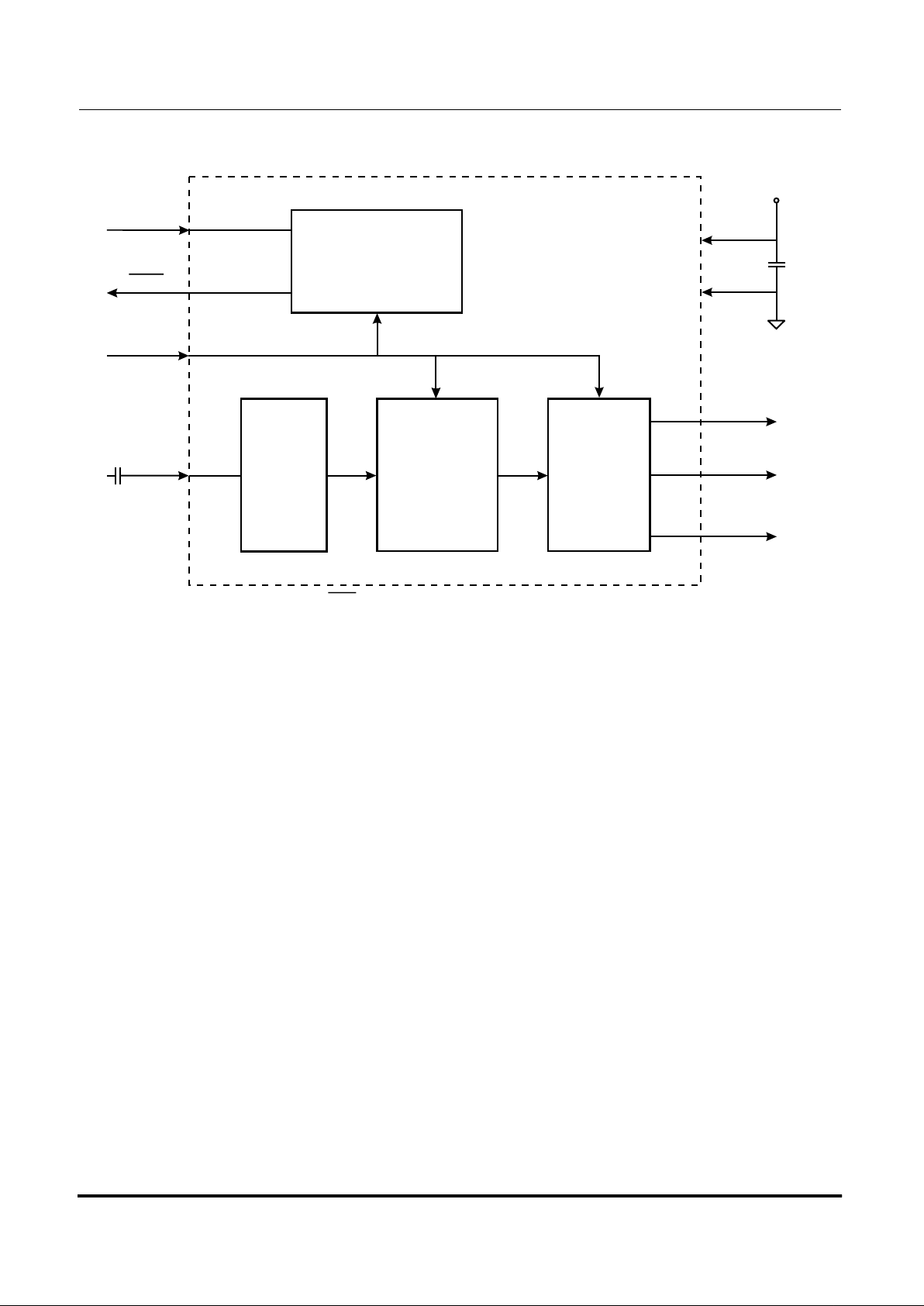
1. Block Diagram
DETECT2
DETECT3
DETECT1
SLICER
SIGIN
ENABLE
XTAL
SIGNAL
ANALYZER
CONTROL
LOGIC
CLOCK
V
SS
V
DD
V
DD
C1
C2
CLOCK /
XTAL
Note: used for 16-pin SOIC (MX643DW) only.XTAL
Figure 1: Block Diagram
Page 4
Call Progress Tone Detector MX643 - Preliminary Information
© 1996 MX•COM, INC. Tele: 800 638 5577, 910 744 5050, Fax: 910 744 5054 Doc. #20480148.001
4
2. Signal List
P-Pin
No.
DW-Pin
No.
Signal Type Description
1 2 CLOCK / XTAL input For the MX643P this is the external clock input to the clock
divider circuit. For the MX643DW this can be either an
external clock input or an external crystal input.
-3
XTAL
output Output of the on-chip oscillator. Not available on 8-pin DIP..
2 4 DETECT3 output When a single tone is within the range of the Call Progress
Band, Non Call Progress Band, or a Special Information
Tone, is detected, this output goes to a logic 1.
3 5 ENABLE input A logic 1 applied to this input enables the decoder and
detection outputs. A logic 0 applied to this input disables the
decoder and forces DETECT1, DETECT2 and DETECT3 to a
logic 0.
4 7 DETECT1 output When a call progress signal is detected, this output goes to a
logic 1.
5 10 SIGIN input Signal input. Signals to this pin should be ac coupled. The dc
bias of this pin is set internally.
612 VSSpower Negative supply. (ground).
7 13 DETECT2 output This output is used in conjunction with DETECT1. When
DETECT1 is at a logic 1, this output goes to a logic 1 if a Call
Progress High Band signal is detected. When DETECT1 is
at a logic 0, this output goes to a logic 1 if a Non Call
Progress signal is detected.
815 VDDpower Positive supply. This pin should be decoupled to VSS by a
capacitor.
1, 6, 8,
9, 11,
14, 16
N/C Internal connection. Do not make a connection to these pins.
Page 5

Call Progress Tone Detector MX643 - Preliminary Information
© 1996 MX•COM, INC. Tele: 800 638 5577, 910 744 5050, Fax: 910 744 5054 Doc. #20480148.001
5
3. External Components
CLOCK
C2
8
7
2
3
4
5
6
DETECT1
MX643P
ENABLE
V
SS
SIGIN
DETECT2
DETECT3
V
DD
C1
1
V
DD
XTAL/
CLOCK
C3
C2
R1
X1
C4
DETECT3
MX643DW
ENABLE
SIGIN
DETECT2
V
DD
V
SS
C1
XTAL
1
2
3
4
5
6
7
8
16
15
14
13
12
11
10
9
DETECT1
N/C
N/C
N/C
N/C
N/C
N/C
N/C
V
DD
MX643P
C1 1.0nF
±20
R1
1MΩ±10
C2
1.0µF ±20
C1 560pF at 3.3V
DD
1.0nF at 5.0V
DD
±20
For details of CLOCK frequency refer to Sec.6.1 C2
1.0µF ±20
C3 33pF
±20
C4 33pF
±20
X1 3.579545MHz refer to Sec. 6.1
Figure 2: Recommended External Components for Typical Applications
4. General Description
4.1 Glossary
The following glossary and Decode Truth table (found in section 5.1), describe the MX643 decoding features and
functions.
Call Progress Tones:
The single and dual frequency tones in the range of 350Hz to 620Hz specified widely for
Call Progress signaling.
Call Progress Band:
The nominal range is 340Hz to 650Hz within which the MX643 will detect Call Progress
tones. The detection algorithm requires that the tones have characteristics typical of Call Progress Tones.
Call Progress Low Band:
The nominal range is 340Hz to 490Hz. The MX643 will detect single or dual tones
falling entirely within this range, as Call Progress Low Band tones.
Call Progress High Band:
The nominal range is 600Hz to 650Hz. Single tones in this range, or dual tones
having a material frequency component within this range (e.g. 480 + 620Hz), are detected as Call Progress High
Band tones.
Special Information Tone:
The nominal range is 950Hz or 1400Hz or 1800Hz, with a tolerance of ±50Hz.
Non Call Progress Signal:
A signal falling within the nominal range (a) 200Hz to 800Hz, but NOT within the Call
Progress Band, or (b) within the nominal range 200Hz to 800Hz, but NOT meeting the DETECTION
REQUIREMENTS when the signal falls in the Call Progress Band.
Subject to the duration and other characteristics of such signals, the MX643 will usually interpret these as a Non
Call Progress Signal (e.g. speech or other signal activity).
Minimum Input Signal:
The minimum signal level for the specified tone decoding performance. The lower level
at which absence of an input signal will be registered is not specified.
No Signal:
A signal falling outside the nominal range of 120Hz to 900Hz or Special Information Tone or the
absence of an input signal. Either will be detected as a No Signal condition.
Page 6

Call Progress Tone Detector MX643 - Preliminary Information
© 1996 MX•COM, INC. Tele: 800 638 5577, 910 744 5050, Fax: 910 744 5054 Doc. #20480148.001
6
Nominal:
Subject to dynamic tolerances within the signal analysis process. Absolute values are not material or
adverse to performance.
4.2 Overall Function Description
The MX643 Call Progress Tone Detector uses different tone detection methods from those commonly found with
other Call Progress Tone Detectors.
Many traditional devices use a bandpass filter followed by an energy detector. The filter is usually designed to
pass input signals with a frequency between about 300Hz and 700Hz. Each signal amplitude in this range is then
checked against a level threshold. Any signal of acceptable level in this frequency band is classed as a Call
Progress tone, including speech and noise. False outputs caused by speech are commonly indicated by such
products and background noise may lead to a stuck detect output.
In contrast, the MX643 uses a stochastic signal processing technique. This technique is based on analysis of both
the frequency and time domains, with signal amplitude forming a minor part in the decision process. This analysis
includes, checks on whether the signal has a profile which matches international standards for Call Progress
Tones, Special Information Tones, or a profile more likely to match that of speech, noise or other Non-Call
Progress signals. Checks are also performed to see if the signal is a single tone, and whether the tones which
include frequencies corresponding with the ‘U.S. Busy’ signals have been detected.
5. Block Diagram Description
(Reference Figure 1)
Slicer
The input signal to the slicer is amplified by a self-biased inverting amplifier. The dc bias of this input is internally
set at V
DD
/2.
Signal Analyzer
The frequency range, quality, and consistency of the input signal is analyzed by this function block. To be
classified as a Call Progress signal the input signal frequencies should lie between 340Hz and 650Hz. To be
classified as a Special Information Tone, the input signal frequency should lie between 900Hz and 1000Hz or
1350Hz and 1450Hz or 1750Hz and 1850Hz. The signal to noise ratio must be 16dB or greater. The signal must
be consistent over a period of about 145 ms. These decode criteria are continuously monitored and the
assessment is updated every 7 ms, reference Figure 3.
The Signal Analyzer samples the call progress signal at 9.3kHz. Care should be taken to avoid high frequency
signals (≥8.4kHz) aliasing into the call progress band.
Control Logic
This block categorizes the nature of the signal into various decoded output states and controls the three output
pins. See the Decode Output Truth Table in section 5.1
Clock
An external clock source is to be connected to the CLOCK input pin when using the 8-pin device. If using the onchip oscillator (16-pin device only) you will need to use the external components shown in Figure 2. If using an
external clock source then
XTAL
should be left unconnected.
Page 7

Call Progress Tone Detector MX643 - Preliminary Information
© 1996 MX•COM, INC. Tele: 800 638 5577, 910 744 5050, Fax: 910 744 5054 Doc. #20480148.001
7
5.1 Decode Output Truth Table
DETECT3 DETECT2 DETECT1 CONDITIONS
0 0 0 No Signal
1 0 0 Special Information Tone: Will detect 950, 1400 and 1800Hz tones
0 0 1 Call Progress Low Band: Will detect 350+440, 400+450 and
440+480Hz tones, for example
1 0 1 Call Progress Low Band: Will detect single 400, 425, 440, and
450Hz tones, for example
0 1 1 Call Progress High Band:
Will detect 480+620Hz tones, for example
1 1 1 Call Progress High Band: Will detect single 600 and 620Hz tones, for
example
0 1 0 Non Call Progress signal, e.g. Voice Activity
1 1 0 Will detect a single tone lying outside the Call Progress Band and
within the Non Call Progress signal range
Decode Output Truth Table Notes:
DETECT1 responds to the complete range of call progress signals from 340Hz to 650Hz
DETECT2 responds to higher frequency call progress and voice or similar activity
DETECT3 responds to and indicates the presence of a single tone
6. Performance Specification
6.1 Electrical Performance
Absolute Maximum Ratings
Exceeding these maximum ratings can result in damage to the device.
General Min. Max. Units
Supply (VDD - VSS) -0.3 7.0 V
Voltage on any pin to V
SS
-0.3 V
DD
+ 0.3 V
Current
V
DD
-30 30 mA
V
SS
-30 30 mA
Any other pin -20 20 mA
P/DW Package
Total Allowable Power Dissipation at T
AMB
= 25°C 800 mW
Derating above 25°C 13 mW/°C above 25°C
Storage Temperature -55 125 °C
Operating Temperature -40 85 °C
Operating Limits
Correct operation of the device outside these limits is not implied.
Notes Min. Max. Units
Supply (VDD - VSS) 3.0 5.5 V
Xtal Frequency 3.57 3.59 MHz
Page 8

Call Progress Tone Detector MX643 - Preliminary Information
© 1996 MX•COM, INC. Tele: 800 638 5577, 910 744 5050, Fax: 910 744 5054 Doc. #20480148.001
8
Operating Characteristics
For the following conditions unless otherwise specified:
Xtal Frequency = 3.579545MHz, S/N = 16 dB, Noise Bandwidth = 5 kHz,
V
DD
= 3.3V to 5.0V, T
AMB
= - 40°C to 85°C. 0dB = 775mV
RMS
.
Notes Min. Typ. Max. Units
DC Parameters
Supply Current
IDD (ENABLE = 1) (VDD = 5.0V) 1 0.5 1.0 mA
IDD (ENABLE = 1) (VDD = 3.3V) 1 0.3 0.7 mA
Enable Input
Input Logic 1 Level 2 80% V
DD
Input Logic 0 Level 2 20% V
DD
Input Leakage Current (VIN = 0 to VDD) 2 -5.0 5.0 µA
Input Capacitance 2 10.0 pF
Detect Output
Output Logic 1 Level (lOH = 120µA) 3 90% V
DD
Output Logic 0 Level (lOL = 360µA) 3 10% V
DD
AC Parameters
SIGIN pin
Input Impedance (at 100Hz) 4 350
k
Ω
Input Signal Level 5 -40 dB
Input Signal Dynamic Range 5 40 dB
Signal to Noise Ratio 16 dB
Clock Input
'High' Pulse Width 6 40 ns
'Low' Pulse Width 6 40 ns
Input Impedance (at 100Hz) 10
M
Ω
Gain (input = 1mV
RMS
at 100Hz) 20 dB
Operating Characteristics Notes:
1. Not including any current drawn from the device pins by external circuitry.
2. ENABLE pin.
3. DETECT1, DETECT2 and DETECT3 pins.
4. Small signal impedance.
5. The input level is not critical as the detector uses a stochastic algorithm.
6. Timing for an external input to the CLOCK pin.
Page 9

Call Progress Tone Detector MX643 - Preliminary Information
© 1996 MX•COM, INC. Tele: 800 638 5577, 910 744 5050, Fax: 910 744 5054 Doc. #20480148.001
9
Timing Characteristics
For the following conditions unless otherwise specified:
Xtal Frequency = 3.579545MHz, V
DD
= 3.3V to 5.0V, T
AMB
= - 40°C to 85°C, S/N = 20dB.
Timing
(ref. Figures 3, 4, 5 and 6)
Notes Min. Typ. Max. Units
t
I
Burst Length Ignored 1 70 ms
t
L
Burst Length Detected 1 145 ms
t
GI
Call Progress Tone Gap Length Ignored 1, 2 20 ms
t
GD
Call Progress Tone Gap Length Detected 1, 2 40 ms
t
RP
Call Progress Tone Response Time 1 145 ms
t
DRP
Call Progress Tone De-response Time 1 145 ms
t
GDR
Gap Detected Recorded 1, 3 6 ms
t
NG
Non Call Progress Signal Gap Length Ignored 4 80 ms
t
NRP
Non Call Progress Signal Response Time 145 ms
t
DNRP
Non Call Progress signal De-response Time 80 ms
t
CH
State Change 0 ms
t
V
DETECT1, DETECT2, and DETECT3 Response
Time
5 145 ms
Timing Notes:
1. Timings also apply to Special Information Tone.
2. Only applies to bursts of the same frequency.
3. To acknowledge a short tone gap ≥ 40 ms, No Signal is indicated for a minimum of 6ms.
4. If the gap > 90 ms, a No Signal state will be decoded.
5. Time between a stable XTAL/CLK and a valid DETECT1, DETECT2, and DETECT3 state when
ENABLE is logic high..
Timing Diagrams
SIGIN
DETECT1
ENABLE
No Signal
Call Progre s s
Low Band
Call Progre s s
High Band
Call Progre s s
High Band
Call Progre s s
High Band
DETECT2
Note: DETECT3 is logic high only when the Call Progress Signal, or the Non Call Progress Signal is a single frequency tone.
t
I
t
L
t
GD
t
DRP
t
GI
t
GDR
t
RP
t
RP
t
RP
t
DRP
DETECT3
Figure 3: Timing Diagram: Call Progress Tone(s)
Page 10

Call Progress Tone Detector MX643 - Preliminary Information
© 1996 MX•COM, INC. Tele: 800 638 5577, 910 744 5050, Fax: 910 744 5054 Doc. #20480148.001
10
SIGIN
DETECT1
ENABLE
No Signal
0 Level
Non Call
Progress Signal
Non Call
Progress Signal
DETECT2
DETECT3
t
NRP
t
I
t
NG
t
L
t
NDRP
Note: DETECT3 is logic high only when the Call Progress Signal, or the Non Call Progress Signal is a single frequency tone.
Figure 4: Timing Diagram: Non Call Progress Signal
SIGIN
DETECT1
ENABLE
No Signal
Call Progre s s
Low Band
Non Call
Progress Signal
Call Progre s s
Low Band
DETECT2
DETECT3
t
DRP
t
CH
t
NRP
t
RP
t
RP
Note: DETECT3 logic high only when the Call Progress signal, or the Non Call Progress signal is a single frequency tone.
Figure 5: Timing Diagram: Call Progress Tone(s) to Non Call Progress Signal
SIGIN
DETECT1
DETECT2
ENABLE
No Signal
Special
Information
Tone
Special
Information
Tone
Special
Information
Tone
Special
Information
Tone
DETECT3
0 Level
0 Level
t
I
t
L
t
GD
t
RP
t
DRP
t
RP
t
GI
t
GDR
t
RP
t
DRP
Figure 6: Timing Diagram: Special Information Tones
Page 11

Call Progress Tone Detector MX643 - Preliminary Information
© 1996 MX•COM, INC. Tele: 800 638 5577, 910 744 5050, Fax: 910 744 5054 Doc. #20480148.001
11
DETECT 1
DETECT 2
DETECT 3
XTAL/CLOCK
t
V
indeterminate signal
valid signal
t = the time at which XTAL/CLOCK becomes stable
S
Figure 7: Timing Diagram: DETECT1, DETECT2, and DETECT3 Response time when ENABLE is high
DETECT 2
DETECT 1
DETECT 3
5V
0V
SITSIT SITSINGLETONE
VOICEVOICE
340Hz
596Hz
701Hz
1041Hz
200Hz
894Hz
1343Hz
1489Hz
1716Hz
1858Hz
896Hz
NOT DRAWNTO SCALE
5V
0V
5V
0V
Figure 8: MX643 Frequency Sweep Results
Page 12

Call Progress Tone Detector MX643 - Preliminary Information
© 1996 MX•COM, INC. Tele: 800 638 5577, 910 744 5050, Fax: 910 744 5054 Doc. #20480148.001
12
6.2 Packaging
A
B
PIN1
MJ1
Y
E1
T
E
K
K1
P
H
C
J
F
L
A
B
C
E
E1
F
H
TYP. MAX.MIN.
DIM.
J
J1
P
Y
T
K1
K
L
M
0.200 (5.06)
0.260 (6.60)
0.390 (9.87).
7°
0.150 (3.81)
0.400 (10.16)
0.145 (3.68)
0.100 (2.54)
0.121 (3.07)
0.020 (0.51)
0.300 (7.62)
0.290 (7.37) 0.325 (8.22)
0.30 (7.62)
0.040 (1.01)
0.008 (0.20) 0.015 (0.38)
0.015 (0.38) 0.023 (0.58)
0.045 (1.14) 0.065 (1.65)
0.060 (1.52)
0.060 (1.52)
0.346 (8.790)
0.240 (6.10)
NOTE: All dimensions in inches (mm.)
Angles are in degrees
Pac kageTolerances
0.015 (0.38)
0.033 (0.84)
Figure 9: 8-pin PDIP Mechanical Outline:
Order as part no. MX643P
PIN 1
A
B
ALTERNATIVE
PIN
LOCA TION
MARKING
X
P
J
Y
C
K
H
E
L
T
W
Z
NOTE: All dimensions in inches (mm.)
Angles are in degrees
Packa geTolerances
A
B
C
E
H
TYP.
MAX.MIN.
DIM.
J
P
X
W
T
Y
K
L
0.105 (2.67)0.093 (2.36)
0.419 (10.64)
45°
7°
0° 10°
0.050 (1.27)
0.041 (1.04)
0.413 (10.49)
0.299 (7.59)
0.050 (1.27)
0.016 (0.41)
0.390 (9.90)
0.020 (0.51)0.003 (0.08)
0.009 (0.23) 0.0125 (0.32)
0.013 (0.33) 0.020 (0.51)
0.395 (10.03)
0.286 (7.26)
Z
5°
5°
Figure 10: 16-pin SOIC Mechanical Outline:
Order as part no. MX643DW
 Loading...