

Page 1
DATA BULLETIN
MX641
Dual SPM Detector
Features Applications
x Two (12kHz / 16kHz) SPM Detectors on a
Single Chip
x Detects 12 or 16kHz SPM Frequencies
x ‘Controlled’ (PC) & ‘Fixed’ Signal Sensitivity
Modes
x Selectable Tone Follower or Packet Mode
Outputs
x High Speech-Band Rejection Properties
x ‘Output Enable’ Multiplexing Facility
XTAL/CLOCK
XTAL
Ch1AMPOUT
Ch1 AMP IN (-)
Ch1 AMP IN (+)
PRESET LEVEL
CHIP SELECT
SERIAL
DATA
SERIAL
CLOCK
SYSTEM SELECT
Ch2 AM PIN (-)
Ch2 AMP IN (+)
Ch2AMPOUT
+
Ch 1
INPUT
AMPLIFIER
SERIAL
INPUT
LOGIC
Ch 2
INPUT
AMPLIFIER
+
XTAL/CLOCK
GENERATOR
Ch 1
BANDPASS
FILTER
GAIN
ADJUST
LEVEL/
SYSTEM
SETTING
GAIN
ADJUST
Ch 2
BANDPASS
FILTER
COMPARATOR
THRESHOLD
COMPARATOR
THRESHOLD
CLOCK OUT CLOCK IN
BUFFER
Ch 1
COMPARATOR
+
INTERNAL
12kHz/16kHz
SYSTEM
INTERNAL
+
-
Ch 2
COMPARATOR
x Call Charge Applications on PABX Line
Cards
x Remote Telephone Applications
CLOCK
DIVIDERS
12kHz/16kHz
PULSE
GENERATOR
AND
DIVIDER
CHANNEL 1
CHANNEL 2
PULSE
GENERATOR
AND
DIVIDER
SYSTEM
PULSE
MEASUREMENT
LOGIC
PULSE
MEASUREMENT
LOGIC
TONE FOLLOWER
PULSE
LENGTH
LOGIC
PULSE
LENGTH
LOGIC
TONE FOLLOWER
PRELIMINARY INFORMATION
V
DD
V
OUTPUT
SELECT
CIRCUITS
OUTPUT
SELECT
CIRCUITS
V
Ch 1
OUTPUT
OUTPUT
ENABLE
OUTPUT
SELECT
Ch 2
OUTPUT
BIAS
SS
MODE
MODE
INTERNAL
CLOCKS
PACKET
MODE
12kHz/16kHz
SYSTEM
PACKET
MODE
The MX641 is a low-power, system-selectable Dual Subscriber Pulse Metering (SPM) Detector designed to indicate the
presence, on a telephone line, of either 12kHz or 16kHz telephone call-charge frequencies. It is designed for PBX and
PABX line-card and remote telephone installations. Under PProcessor control via a common serial interface, each
channel of the MX641 will detect call-charge pulses from a telephone line and provide a digital output for recording, billing
or security purposes. A common set of external components and a stable 3.579545MHz Xtal/clock input ensures that the
MX641 adheres accurately to most national “Must and Must-Not” decode band-edges and threshold levels. For nonPProcessor systems a preset sensitivity/system input allows external channel level and system setting
The digital output is pin-selectable to one of three modes:
(1) Tone Follower mode: logic level for the period of a correct decode.
(2) Packet mode: respond/de-respond after a cumulative period of tone or notone in a fixed (intrinsic hardwired period
that is not user controlled) period.
(3) High-impedance output: for device multiplexing.
The MX641 requires a 5V supply and is available in the following packages: 24-pin SOIC (MX641DW) and 24-pin PDIP
(MX641P).
© 1998 MX
4800 Bethania Station Road, Winston-Salem, NC 27105-1201 USA All trademarks and service marks are held by their respective companies.
xCOM Inc. www.mxcom.com Tele: 800 638-5577 910 744-5050 Fax: 910 744-5054 Doc. # 20480115.003
Page 2

Dual SPM Detector 2 MX641 PRELIMINARY INFORMATION
CONTENTS
Section Page
1. Block Diagram.................................................................................................................................. 3
2. Signal List......................................................................................................................................... 4
3. External Components...................................................................................................................... 6
4. General Description......................................................................................................................... 7
4.1 Xtal/Clock Distribution............................................................................................................................... 7
4.2 Channel Outputs....................................................................................................................................... 7
4.3 Sensitivity Setting...................................................................................................................................... 8
4.3.1 Controlled Sensitivity Setting.............................................................................................................................8
4.3.2 Fixed Sensitivity Setting....................................................................................................................................11
5. Applications .................................................................................................................................... 12
5.1.1 Input Configurations..........................................................................................................................................12
5.1.2 Protection Against High Voltages .....................................................................................................................12
5.1.3 Aliasing .............................................................................................................................................................12
6. Performance Specification............................................................................................................. 13
6.1 Electrical Specifications ........................................................................................................................... 13
6.1.1 Absolute Maximum Ratings..............................................................................................................................13
6.1.2 Operating Limits................................................................................................................................................13
6.1.3 Operating Characteristics .................................................................................................................................13
6.2 Timing ...................................................................................................................................................... 15
6.3 Packages ................................................................................................................................................. 16
MXxCOM, Inc. reserves the right to change specifications at any time and without notice.
© 1998 MXxCOM Inc. www.mxcom.com Tele: 800 638-5577 910 744-5050 Fax: 910 744-5054 Doc. # 20480115.003
4800 Bethania Station Road, Winston-Salem, NC 27105-1201 USA All trademarks and service marks are held by their respective companies.
Page 3
Dual SPM Detector 3 MX641 PRELIMINARY INFORMATION
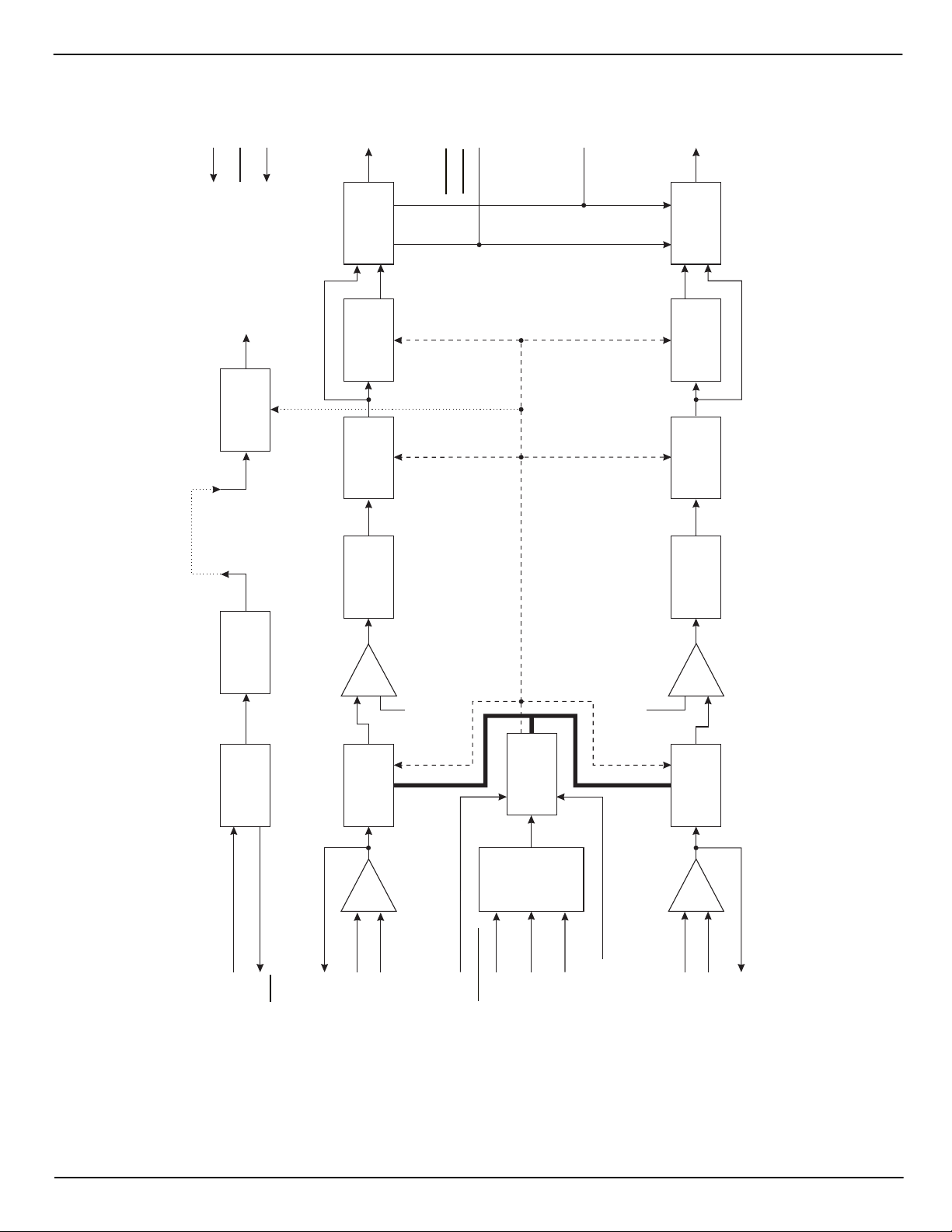
1. Block Diagram
DDVBIASVSS
V
CLOCKS
INTERNAL
CLOCK
DIVIDERS
TONE FOLLOWER
SYSTEM
12kHz/16kHz
Ch 1
MODE
OUTPUT
OUTPUT
PULSE
PULSE
MEASUREMENT
PULSE
GENERATOR
SELECT
CIRCUITS
LOGIC
LENGTH
LOGIC
AND
DIVIDER
MODE
PACKET
CHANNEL 1
ENABLE
OUTPUT
SYSTEM
12kHz/16kHz
SELECT
OUTPUT
CHANNEL 2
MODE
PACKET
SELECT
OUTPUT
CIRCUITS
LOGIC
PULSE
LENGTH
LOGIC
PULSE
MEASUREMENT
AND
PULSE
DIVIDER
GENERATOR
Ch 2
OUTPUT
TONE FOLLOWER
MODE
CLOCK OUT CLOCK IN
XTAL/CLOCK
XTAL/CLOCK
BUFFER
GENERATOR
XTAL
SYSTEM
12kHz/16kHz
-
Ch 1
COMPARATOR
Ch1AMPOUT
+
INTERNAL
THRESHOLD
COMPARATOR
LEVEL/
SERIAL
DATA
SERIAL
SYSTEM
SETTING
INPUT
LOGIC
Ch 1
FILTER
BANDPASS
-
Ch1 AMP IN (-)
GAIN
ADJUST
Ch 1
INPUT
+
AMPLIFIER
PRESET LEVEL
Ch1 AMP IN (+)
CHIP SELECT
SERIAL
CLOCK
INTERNAL
THRESHOLD
COMPARATOR
GAIN
Ch 2
SYSTEM SELECT
ADJUST
INPUT
AMPLIFIER
-
+
Ch 2
-
Ch2 AMP IN (-)
BANDPASS
+
FILTER
Ch 2
COMPARATOR
Ch2AMPOUT
Ch2 AMP IN (+)
Figure 1: Block Diagram
© 1998 MXxCOM Inc. www.mxcom.com Tele: 800 638-5577 910 744-5050 Fax: 910 744-5054 Doc. # 20480115.003
4800 Bethania Station Road, Winston-Salem, NC 27105-1201 USA All trademarks and service marks are held by their respective companies.
Page 4

Dual SPM Detector 4 MX641 PRELIMINARY INFORMATION
2. Signal List
Pin No. Name Type Description
1 Xtal/Clock input The input to the on-chip clock oscillator; for use with a 3.579545MHz Xtal in
conjunction with the Xtal output; circuit components are on-chip. When using a
Xtal input, the Clock Out pin should be connected directly to the Clock In pin. If
a clock pulse input is used at the Clock In pin, this (Xtal/Clock) pin must be
connected directly to V
frequency distribution.
2
XTAL
output The output of the on-chip clock oscillator inverter.
3 Clock Out output The buffered output of the on-chip-clock oscillator inverter. If a Xtal input is
used, this output should be connected directly to the Clock In pin. This output
can support up to 3 additional MX641 ICs. See Figure 3 for details of clock
frequency distribution.
4 Clock In input The 3.579545 clock pulse input to the internal clock dividers. If an externally
generated clock pulse input is used, the Xtal/Clock input pin should be
connected to V
5
Output Enable
input For multi-chip output multiplexing; controls the state of both Ch1 and Ch2
DD
.
outputs. When this input is placed high (logic '1') both outputs are set to a high
impedance. When placed low (logic '0') both outputs are enabled.
6 Ch 2 Output output The digital output of the Channel 2 SPM detector when enabled. The format of
the signal at this pin, in common with Ch 1, is selectable to either
'Tone Follower' or 'Packet' mode via the Output Select input.
7 Ch 1 Output output The digital output of the Channel 1 SPM detector when enabled. The format of
the signal at this pin, in common with Ch 2, is selectable to either
'Tone Follower' or 'Packet' mode via the Output Select input.
8V
BIAS
power The output of the on-chip analog bias circuitry. Held internally at VDD/2, this
pin should be decoupled to V
9 Ch 1 Amp Out output The output of the Channel 1 Input Amplifier. See Figure 2 and Figure 8.
10 Ch 1 Amp In (-): input The negative input to the Channel 1 Input Amplifier. See Figure 2 and Figure
8.
11 Ch 1 Amp In (+): input The positive input to the Channel 1 Input Amplifier. See Figure 2 and Figure 8.
12 V
SS
power Negative supply (GND).
13 N/C No internal connection; leave open circuit.
14 Ch 2 Amp In (+): input The positive input to the Channel 2 Input Amplifier. See Figure 2 and Figure 8.
15 Ch 2 Amp In (-): input The negative input to the Channel 2 Input Amplifier. See Figure 2 and Figure
8.
16 Ch 2 Amp Out output The output of the Channel 2 Input Amplifier. See Figure 2 and Figure 8.
17 Output Select input A logic input to set the Channel 1 and Channel 2 output modes. When high
(logic '1'), the outputs are in the Tone Follower mode; when low (logic '0'), the
outputs are in the Packet mode.
18 Preset Level input A logic input to set the sensitivity mode of the MX641. When high (logic '1'),
both channels are in the Fixed Sensitivity mode. The external components
govern the input sensitivity; the System Select input selects 12kHz or 16kHz
operation. When low (logic '0'), both channels are in the Controlled Sensitivity
mode. Device sensitivities and system selection are via the Chip Select/Serial
Data/Serial Clock inputs. This input has an internal pullup resistor on chip
(Fixed Sensitivity Mode).
19
Chip Select
input The Chip Select input for use in data loading when using the MX641 in the
Controlled Sensitivity mode (see Figure 9). The device is selected when this
input is set low (logic '0'). When the MX641 is in the Fixed Sensitivity mode
this input should be connected to either V
(see Figure 2). See Figure 3 for details of clock
DD
(see Figure 2).
SS
or VDD.
SS
© 1998 MXxCOM Inc. www.mxcom.com Tele: 800 638-5577 910 744-5050 Fax: 910 744-5054 Doc. # 20480115.003
4800 Bethania Station Road, Winston-Salem, NC 27105-1201 USA All trademarks and service marks are held by their respective companies.
Page 5

Dual SPM Detector 5 MX641 PRELIMINARY INFORMATION
Pin No. Name Type Description
20 Serial Clock input The Serial Clock input for use in data loading when using the MX641 in the
Controlled Sensitivity mode (see Figure 9). Data is loaded to the MX641 on
this clock's rising edge. When the MX641 is in the Fixed Sensitivity mode this
input should be connected to either V
or VDD.
SS
21 Serial Data input The Serial Data input for use in data loading when using the MX641 in the
Controlled Sensitivity mode (see Figure 9 and Table 4). When the device is in
the Fixed Sensitivity mode this input should be connected to either V
or VDD.
SS
22 System Select input In the Fixed Sensitivity mode this pin selects the system frequency. High (logic
‘1’) = 12kHz; Low (logic ‘0’) = 16kHz. In the Controlled Sensitivity mode this pin
is inactive and may be left unconnected. This pin has an internal pullup
resistor on chip.
23 N/C No internal connection; leave open circuit.
24 V
DD
power Positive supply rail; a single, stable power supply is required. Critical levels
and voltages within the MX641 are dependent upon this supply. This pin
should be decoupled to V
by a capacitor mounted close to the pin
SS
Table 1: Signal List
© 1998 MXxCOM Inc. www.mxcom.com Tele: 800 638-5577 910 744-5050 Fax: 910 744-5054 Doc. # 20480115.003
4800 Bethania Station Road, Winston-Salem, NC 27105-1201 USA All trademarks and service marks are held by their respective companies.
Page 6

Dual SPM Detector 6 MX641 PRELIMINARY INFORMATION
3. External Components
V
DD
If you use a Clock Pulse input:
- Remove Xtal (X )
- Connect Pin 1 to V
- Do not short Pins 3 & 4
- Input clock pulses to CLOCK IN
See Figure 3
1
DD
CLOCK IN
C3
C4
C2
CH1 AMP IN (-)
CH1 AMP IN (+)
R8
XTAL/CLOCKXTAL/CLOCK
X1
XTAL
CLOCK
OUTPUT ENABLE
CH2 OUTPUT
CH1 OUTPUT
CH1 AMP OUT
R2
OUT
IN
V
R1
R4
BIAS
R3
V
SS
1
2
3
4
5
6
MX641
7
8
9
10
11
12
24
23
22
21
20
19
18
17
16
15
14
13
V
DD
SYSTEM SELECT
SERIAL DATA
SERIAL CLOCK
CHIP SELECT
PRESET LEVEL
OUTPUT SELECT
CH2 AMP OUT
R7
CH2 AMP IN (-)
R6
CH2 AMP IN (+)
R5
C1
V
DD
C5
C6
Figure 2: Recommended External Components
R1
R2
R3 Note 1
R4 Note 1
R5
R6
R7 Note 1
R8 Note 1
68k
68k:
750k:
750k:
68k:
68k:
750k:
750k:
± 1% C1 1.0µF ±20%
:
±1% C2 1.0µF ±20%
±1% C3 270pF ±5%
±1% C4 270pF ±5%
± 1% C5 270pF ±5%
± 1% C6 270pF ±5%
±1%
±1% X1 Note 2, 3 3.579545MHz
Table 2: Recommended External Components
Note:
1. Fixed Sensitivity Setting: when calculating/selecting gain components, R3,
R4, R7 and R8 should always be
greater than or equal to 100k:.
2. For best results, a crystal oscillator design should drive the clock inverter input with signal levels of at least 40% of
, peak to peak. Tuning fork crystals generally cannot meet this requirement. To obtain crystal oscillator design
V
DD
assistance, consult your crystal manufacturer.
3. The on-chip crystal circuitry includes a feedback resistor (nominally 2M:) between pins 1 & 2 and load capacitors
on pins 1 & 2 (nominally 10pF each, excluding package and board parasitics).
© 1998 MXxCOM Inc. www.mxcom.com Tele: 800 638-5577 910 744-5050 Fax: 910 744-5054 Doc. # 20480115.003
4800 Bethania Station Road, Winston-Salem, NC 27105-1201 USA All trademarks and service marks are held by their respective companies.
Page 7

Dual SPM Detector 7 MX641 PRELIMINARY INFORMATION
4. General Description
4.1 Xtal/Clock Distribution
The MX641 requires a 3.579545MHz Xtal or clock pulse input. With the exception of the Xtal, all oscillator components
are incorporated on chip. If a Xtal input is employed the Clock Out pin should be directly linked to the Clock In pin.
To reduce component and layout complexity, the clock requirements of up to 3 additional MX641 microcircuits may be
supplied from a Xtal-driven MX641 acting as the system master clock. With reference to Figure 3, the clock should be
distributed as illustrated and the Xtal/Clock pins of the driven microcircuits should be connected directly to V
Note (see section 6.1.3) that the maximum load on the master Clock Out pin should not be exceeded.
DD
.
µController
Ch 2
I/O Ports
Ch 1
XTAL/CLOCK
X1
3 to'N' LINE
DECODER
"OUTPUT ENABLE"
ADDRESSING
XTAL
CLOCK
OUT
MX641
(used as
Master
Oscillator)
Ch 1
CLOCK
IN
Ch 2
CLOCK
IN
XTAL/CLOCK
MX641 MX641 MX641
Ch 1
V
DD
XTAL/CLOCK
Ch 2
CLOCK
IN
Ch 1
XTAL/CLOCK
Ch 2
OUTPUT
ENABLE
CLOCK
IN
Ch 1 OUTPUT
Ch 2 OUTPUT
Figure 3: Xtal/Clock Distribution and Output Multiplexing
4.2 Channel Outputs
Channel 1 and Channel 2 outputs operate together under the control of the Output Enable and Output Select inputs.
Table 3 describes the operations.
The digital output is pin-selectable to one of three modes:
(1) Tone Follower mode: a logic level for the period of a correct decode.
(2) Packet mode: respond/de-respond after a cumulative period of tone or notone in a fixed (intrinsic hardwired period
that is not user controlled) period.
(3) High-impedance output: for device multiplexing.
System
Select
Preset
Level
Output
Select
Output
Enable
Operating Mode
Mode Sensitivity Frequency
X 0 0 0 Packet Mode Output; Serial Data Control (see note)
X 0 1 0 Tone Follower Output; Serial Data Control (see note)
0 1 0 0 Packet Mode Output; Fixed Sensitivity 16kHz
1 1 0 0 Packet Mode Output; Fixed Sensitivity 12kHz
0 1 1 0 Tone Follower Output; Fixed Sensitivity 16kHz
1 1 1 0 Tone Follower Output; Fixed Sensitivity 12kHz
X X X 1 Tristate Output (High Z)
X = don’t care
Note: Device sensitivity and system frequency must be serially loaded
Table 3: Operating Mode Configuration
© 1998 MXxCOM Inc. www.mxcom.com Tele: 800 638-5577 910 744-5050 Fax: 910 744-5054 Doc. # 20480115.003
4800 Bethania Station Road, Winston-Salem, NC 27105-1201 USA All trademarks and service marks are held by their respective companies.
Page 8

Dual SPM Detector 8 MX641 PRELIMINARY INFORMATION
SIGNAL INPUT
CH1 and CH 2 OUTPUTS
TONE FOLLOWER OUTPUT
PACKET MODE OUTPUT
SIGNAL INPUT ......
TONE F O L L OWER OUTPUT ......
PACKE T MODE OUTPUT ......
Figure 4: Tone Follower and Packet Mode Outputs
TONE NOTONE
RESPONSE
DELA Y
DERESPONSE
DELA Y
4.3 Sensitivity Setting
To enable the MX641 to operate correctly to most national 12kHz and 16kHz SPM specifications, the input sensitivity can
be accurately adjusted and set.
There are two different pin-selectable modes of sensitivity setting available to the MX641: Controlled Sensitivity Mode and
Fixed Sensitivity Mode
The Controlled Sensitivity mode allows the sensitivity setting from a µController via a 6-bit serial data input. This same
serial input also sets operation (bit 0) to either 12kHz or 16kHz systems. Both channels are set identically.
The Fixed Sensitivity mode allows the sensitivity of each channel to be set to a fixed “gain” by external components at the
input amplifiers. Operation to either 12kHz or 16kHz is by the System Select input.
4.3.1 Controlled Sensitivity Setting
With the external gain (sensitivity) components used as shown in Figure 2, the gain of the input stages is 19.8dB (12kHz)
or 20.5dB (16kHz). For controlled sensitivity setting the gain of each bandpass filter, and therefore the device sensitivity,
is adjusted by the applied serial bits D1 to D5.
In the Controlled Sensitivity mode the system frequency is selected by bit D0 (‘1’ = 12kHz; ‘0’ = 16kHz). Data is loaded
Bit 5 (D5) first. Table 4 details the serial data inputs for the required sensitivity. Minimum, Nominal and Maximum
Sensitivity figures are provided to make complete allowance for internal circuit offsets and component tolerances.
0dB(ref.) = 775mV
Note: Device sensitivity is directly proportional to V
at VDD = 5.0 volts; varies directly with VDD.
RMS
DD
© 1998 MXxCOM Inc. www.mxcom.com Tele: 800 638-5577 910 744-5050 Fax: 910 744-5054 Doc. # 20480115.003
4800 Bethania Station Road, Winston-Salem, NC 27105-1201 USA All trademarks and service marks are held by their respective companies.
Page 9

Dual SPM Detector 9 MX641 PRELIMINARY INFORMATION
4.3.1.1 Controlled Sensitivity Setting Information
The sensitivity figures in Table 4 are based on the following:
1. The recommended amplifier components (see Figure 2) are used, providing an amplifier gain at 16kHz
of 19.8dB ±0.3dB or at 12kHz of 19.1dB ±0.3dB.
2. A comparator sensitivity of 1.6dB(ref.) ±1dB (the variation is due to filter gain error, filter output offset, comparator
input offset or a combination of all 3).
3. The applied V
is 5.0 volts; 0dB (ref.) = 775mV
DD
RMS
.
Serial Data
Bits
Bandpass
Filter Gain
Minimum
Sensitivity
12kHz System
Bit D0 = ‘1’
Nominal
Sensitivity
Maximum
Sensitivity
Minimum
Sensitivity
16kHz System
Bit D0 = ‘0’
Nominal
Sensitivity
Maximum
Sensitivity
D5 - D1 (dB) dB(ref.) dB(ref.) dB(ref.) dB(ref.) dB(ref.) dB(ref.)
00000 0 -16.2 -17.5 -18.8 -16.9 -18.2 -19.5
00001 1.0 -17.2 -18.5 -19.8 -17.9 -19.2 -20.5
00010 2.0 -18.2 -19.5 -20.8 -18.9 -20.2 -21.5
00011 3.0 -19.2 -20.5 -21.8 -19.9 -21.2 -22.5
00100 4.0 -20.2 -21.5 -22.8 -20.9 -22.2 -23.5
00101 5.0 -21.2 -22.5 -23.8 -21.9 -23.2 -24.5
00110 6.0 -22.2 -23.5 -24.8 -22.9 -24.2 -25.5
00111 7.0 -23.2 -24.5 -25.8 -23.9 -25.2 -26.5
01000 8.0 -24.2 -25.5 -26.8 -24.9 -26.2 -27.5
01001 9.0 -25.2 -26.5 -27.8 -25.9 -27.2 -28.5
01010 10.0 -26.2 -27.5 -28.8 -26.9 -28.2 -29.5
01011 11.0 -27.2 -28.5 -29.8 -27.9 -29.2 -30.5
01100 12.0 -28.2 -29.5 -30.8 -28.9 -30.2 -31.5
01101 13.0 -29.2 -30.5 -31.8 -29.9 -31.2 -32.5
01110 14.0 -30.2 -31.5 -32.8 -30.9 -32.2 -33.5
01111 15.0 -31.2 -32.5 -33.8 -31.9 -33.2 -34.5
10000 16.0 -32.2 -33.5 -34.8 -32.9 -34.2 -35.5
10001 17.0 -33.2 -34.5 -35.8 -33.9 -35.2 -36.5
10010 18.0 -34.2 -35.5 -36.8 -34.9 -36.2 -37.5
10011 19.0 -35.2 -36.5 -37.8 -35.9 -37.2 -38.5
10100 20.0 -36.2 -37.5 -38.8 -36.9 -38.2 -39.5
10101 21.0 -37.2 -38.5 -39.8 -37.9 -39.2 -40.5
10110 22.0 -38.2 -39.5 -40.8 -38.9 -40.2 -41.5
10111 23.0 -39.2 -40.5 -41.8 -39.9 -41.2 -42.5
11000 24.0 -40.2 -41.5 -42.8 -40.9 -42.2 -43.5
11001 25.0 -41.2 -42.5 -43.8 -41.9 -43.2 -44.5
11010 26.0 -42.2 -43.5 -44.8 -42.9 -44.2 -45.5
11011 27.0 -43.2 -44.5 -45.8 -43.9 -45.2 -46.5
11100
11101
11110
These states should never be used. If sensitivities of this order are required (e.g. the Swedish
Rural SPM specification), it is recommended that the Controlled Sensitivity setting be set to 20dB
(10100) and external components selected to set the Input Amp gain to a higher figure. This
action will prevent falsing by sub-harmonic frequencies.
11111
Table 4: Controlled Sensitivity Setting Information
© 1998 MXxCOM Inc. www.mxcom.com Tele: 800 638-5577 910 744-5050 Fax: 910 744-5054 Doc. # 20480115.003
4800 Bethania Station Road, Winston-Salem, NC 27105-1201 USA All trademarks and service marks are held by their respective companies.
Page 10

Dual SPM Detector 10 MX641 PRELIMINARY INFORMATION
4.3.1.2 German FTZ Specification (16kHz)
The FTZ system has a Must Decode level of -21dB (ref.) and a Must-Not Decode level of -27dB (ref.). Reference to
Table 4 shows that Bandpass Filter Gain settings of 5dB, 6dB or 7dB will enable an MX641 channel to meet this level
specification. Figure 5 illustrates the range of these various settings.
To meet the German FTZ specification, the input data (D5 to D0) must be:
0 0 1 0 1 0 5.0dB
or 0 0 1 1 0 0 6.0dB
or 0 0 1 1 1 0 7.0dB
Note:
1. By selecting the middle setting, the greatest noise immunity is achieved.
MUST DECODE
-21.9
-23.2 5.0dB
-24.5
MUST -NO T DECODE
WILL DECODE
-22.9
-24.2 6.0dB
-25.5
WILL-NOT DECODE
-21dB(ref.)
-23.9
-25.2 7.0dB
-26.5
-27dB(ref.)
Figure 5: German Specification - Possible Settings
4.3.1.3 French Specification (12kHz)
This system has a Must Decode level of -17.36dB (ref.) and a Must-Not Decode level of -23.8dB (ref.). Reference to
Table 4 shows that Bandpass Filter Gain settings of 2dB, 3dB or 4dB will enable an MX641 channel to meet this level
specification. Figure 6 illustrates the range of these various settings.
To meet the French SPM specification, the input data (D5 to D0) must be:
0 0 0 1 0 1 2.0dB
or 0 0 0 1 1 1 3.0dB
or 0 0 1 0 0 1 4.0dB
Note:
1. By selecting the middle setting, the greatest noise immunity is achieved.
MUST DECODE
-18.2
-19.5 2.0dB
-20.8
WILL-NOT DECODE
MUST -NO T DECODE
WILL DECODE
-19.2
-20.5 3.0dB
-21.8
-17.36dB(ref.)
-20.2
-21.5 4.0dB
-22.8
-23.8dB(ref.)
Figure 6: French Specifications - Possible Settings
© 1998 MXxCOM Inc. www.mxcom.com Tele: 800 638-5577 910 744-5050 Fax: 910 744-5054 Doc. # 20480115.003
4800 Bethania Station Road, Winston-Salem, NC 27105-1201 USA All trademarks and service marks are held by their respective companies.
Page 11

Dual SPM Detector 11 MX641 PRELIMINARY INFORMATION
4.3.2 Fixed Sensitivity Setting
In this mode the sensitivity of each channel is set by the correct selection of the components around the Channel Input
Amplifier. Note that the device sensitivity is directly proportional to the applied power supply (V
bandwidth product of the input opamp can attenuate the SPM signal gain at some input gain configurations.
4.3.2.1 Input Gain Calculation
The input amplifier, with external circuitry, is used to set the sensitivity of the MX641 to conform to the user's national level
specification with regard to ‘Must’ and ‘Must-Not’ decode signal levels.
With reference to the graph in Figure 7, the following steps will assist in the determination of the required gain/attenuation.
Step 1 Draw two horizontal lines from the Y-axis (Signal Level) in Figure 7. The upper line represents the required
‘Must’ decode level. The lower line represents the required ‘Must-Not’ decode level
Step 2 Mark the intersection of the upper horizontal line and the upper sloping line; drop a vertical line from this point to
the X-axis (Amplifier Gain (dB)). The point where the vertical line meets the X-axis indicates the minimum Input
Amp gain required for reliable decoding of valid signals
Step 3 Mark the intersection of the lower horizontal line and the lower sloping line; drop a vertical line from this point to
the X-axis. The point where the vertical line meets the X-axis will indicate the maximum allowable Input Amp
gain. Input signals at or below the ‘Must-Not’ decode level will not be detected as long as the amplifier gain is
no higher than this level.
-10
) and that the gain
DD
-15
RMS
-20
MUST DECODE LEVEL
-25
-30
-35
-40
SIGNAL LEVEL (dB): 0dB ref = 775mV
-45
-50
MUST-NOT DECODE LEVEL
MINIMUM AMPLIFIER GAIN
-20 -15 -10
MAXIMUM AMPLIFIER GAIN
-5
V = 5.0 (±0.1) VOLTS; TEMP = -40°C to 85°C
DD
0
AMPLIFIER GAIN (dB)
5
10 15 20 25
Figure 7: Input Gain Calculation Graph for use in the Fixed Sensitivity Mode
4.3.2.2 Input Gain Components
Refer to the gain components shown in Figure 2. The user should calculate and select external components (R1/R3/C3,
R2/R4/C4 and R5/R7/C5, R6/R8/C6) to provide amplifier gains within the limits obtained in Steps 2 and 3.
Component tolerances should not move the gain-figure outside these limits. The graph in Figure 7 is for the calculation of
input gain components for an MX641 using a V
of 5.0 (±0.1) volts.
DD
It is recommended that the designed gain is near the center of the calculated range.
© 1998 MXxCOM Inc. www.mxcom.com Tele: 800 638-5577 910 744-5050 Fax: 910 744-5054 Doc. # 20480115.003
4800 Bethania Station Road, Winston-Salem, NC 27105-1201 USA All trademarks and service marks are held by their respective companies.
Page 12

Dual SPM Detector 12 MX641 PRELIMINARY INFORMATION
5. Applications
5.1.1 Input Configurations
Tip (a)
Ring (b)
Differential Input
INPUT AMP
+
V
BIAS
MX641
Common Mode Input
INPUT AMP
+
MX641
V
BIAS
Figure 8: Input Configurations
5.1.2 Protection Against High Voltages
Telephone systems may have high d.c. and a.c. voltages present on the line. If the MX641 is part of a host equipment
that has its own signal input protection circuitry, there will be no need for further protection as long as the voltage on any
pin is limited to within V
If the host system does not have input protection, or there are signals present outside the device's specified limits, the
MX641 will require protection diodes at its signal inputs (+ and -). The breakdown voltage of capacitors and the peak
inverse voltage of the diodes must be sufficient to withstand the sum of the d.c. voltages plus all expected signal peaks.
+0.3V and VSS -0.3V.
DD
5.1.3 Aliasing
Due to the sampling nature of switched-capacitor filters used in the MX641, high frequency noise or unwanted signals can
alias into the passband, disrupting detection. External components must be chosen carefully to avoid alias effects.
Possible Alias Frequencies:
12kHz Mode = 52kHz
16kHz Mode = 69kHz
If other filtering in the system has not attenuated these alias frequencies, capacitors should be employed across resistors
R3, R4, R7 and R8 to provide anti-alias filtering.
The low-pass cutoff frequency should be chosen to be approximately 20kHz to 25kHz for a 12kHz system, or 25kHz to
30kHz for a 16kHz system.
i.e.
C
2S
When anti-alias capacitors are used, an allowance must be made for reduced gain at the SPM frequency (12kHz or
16kHz).
1
f
uu u
2
R3
© 1998 MXxCOM Inc. www.mxcom.com Tele: 800 638-5577 910 744-5050 Fax: 910 744-5054 Doc. # 20480115.003
4800 Bethania Station Road, Winston-Salem, NC 27105-1201 USA All trademarks and service marks are held by their respective companies.
Page 13

Dual SPM Detector 13 MX641 PRELIMINARY INFORMATION
6. Performance Specification
6.1 Electrical Specifications
6.1.1 Absolute Maximum Ratings
Exceeding the maximum rating can result in device damage.
Parameter Min. Typ. Max. Unit
Supply Voltage (VDD-VSS) -0.3 7.0 V
Voltage on any pin to V
SS
Current
V
DD
V
SS
Any other pin -20 20 mA
DW / P Packages
Total allowable device dissipation at T
Derating above T
AMB
25qC
AMB
25
qC
Operating Temperature -40 85
Storage Temperature -40 85
-0.3 (VDD + 0.3) V
-30 30 mA
-30 30 mA
800 mW
10
mW/qC above T
qC
qC
AMB
25qC
6.1.2 Operating Limits
Correct Operation of the device outside these limits is not implied.
Parameter Min. Typ. Max. Unit
Supply Voltage (VDD) 4.5 5.0 5.5 V
Operating Temperature -40 85
Xtal/Clock Frequency 3.558918 3.589368 MHz
6.1.3 Operating Characteristics
All device characteristics are measured under the following conditions unless otherwise specified:
V
= 5.0V @ T
DD
Audio Level 0dB (ref.) = 775mV
Xtal/Clock Frequency = 3.579545MHz, System Setting = 12kHz or 16kHz
Supply Current 2.0 5.0 mA
Input/Output Parameters
Clock Out Load 17 15.0 pF
Logic Inputs
Input Logic ‘1’ (High) 3.5 V
Input Logic ‘0’ (Low) 1.5 V
Input Leakage Current (VIN = 0 to VDD)13-5.05.0
Input Current (VIN = 0) 14 -15.0
AMB
= 25qC
, Noise Bandwidth = 50kHz
RMS
Notes Min. Typ. Max. Units
PA
PA
© 1998 MXxCOM Inc. www.mxcom.com Tele: 800 638-5577 910 744-5050 Fax: 910 744-5054 Doc. # 20480115.003
4800 Bethania Station Road, Winston-Salem, NC 27105-1201 USA All trademarks and service marks are held by their respective companies.
Page 14

Dual SPM Detector 14 MX641 PRELIMINARY INFORMATION
Notes Min. Typ. Max. Units
Channel Outputs
Output Logic ‘1’ IOH = 120mA (Enabled) 1 4.6 V
Output Logic ‘0’ IOL = 360mA (Enabled) 1 0.4 V
Output Leakage Current High-Z Output 2 -5.0 5.0
A
P
Input Amplifier
D. C. Gain 60.0 dB
Bandwidth (-3dB) 100 Hz
Input Impedance 1.0
M
:
Overall Performance
12kHz Detect Bandwidth 3 11.82 12.18 kHz
12kHz Not-detect Frequencies (Below 12kHz) 3 11.52 kHz
12kHz Not-detect Frequencies (Above 12kHz) 3 12.48 kHz
16kHz Detect Bandwidth 3 15.76 16.24
16kHz Upper Decode Band Edge (Below 16kHz) 3 15.36 kHz
16kHz Lower Decode Band Edge (Above 16kHz) 3 16.64 kHz
Level Sensitivity
Controlled Sensitivity Mode 3,4,12,15 2.6 1.6 0.6 dB(ref.)
Preset Sensitivity Mode 3,4,5,16 -25.4 -26.4 -27.4 dB(ref.)
Signal Quality Requirements
Signal-to-Noise (Amp Input) 4,8,9,10 22.0 20.0 dB
Signal-to-Voice (Amp Input) 4,8,9,11 -36.0 -40.0 dB
Signal-to-Voice (Amp Output) 4,8,10,11 -1.0 -27.0 dB
Channel Outputs (Ch1 and Ch2) Figure 4
Mode Change Time 6 500 ns
Tone Follower Mode (Table 3)
Response and De-Response Time 3, 4, 7 10.0 ms
Packet Mode (Table 3)
Response and De-Response Time 3, 4, 7 40.0 48.0 ms
Note:
1. Tone Follower or Packet mode enabled; see Table 3
2. Tristate selected; see Table 3.
3. With adherence to Signal-to-Voice and Signal-to Noise specifications.
4. 12kHz and/or 16kHz system.
5. With Input Amp gain setting = 0dB.
6. Time taken to change between any two of the operational modes: Tone Follower, Packet or Tristate, and with a
maximum capacitive load of 30pF on an output.
7. The time delay, after a valid serial data load (or after device powerup), before the condition of the outputs can be
guaranteed correct.
8. Immunity to false responses and/or de-responses.
9. Common Mode SPM and balanced voice input signal.
10. With SPM and voice signal amplitudes balanced; to avoid false de-responses due to saturation, the peak-to-peak
voice + noise level at the output of the Input Amp should be no greater than the dynamic range of the device. For
this reason, the signal-to-voice figure at the AMP Output will vary with the sensitivity setting. The lowest
signal-to-voice figure occurs at the highest sensitivity setting. (Table 4 27dB)
© 1998 MXxCOM Inc. www.mxcom.com Tele: 800 638-5577 910 744-5050 Fax: 910 744-5054 Doc. # 20480115.003
4800 Bethania Station Road, Winston-Salem, NC 27105-1201 USA All trademarks and service marks are held by their respective companies.
Page 15

Dual SPM Detector 15 MX641 PRELIMINARY INFORMATION
11. Maximum voice frequencies = 3.4kHz.
12. With the Input Amplifier gain at 0dB and the Bandpass Filter gain set at 0dB (Table 4); subtract 1.0dB from this
specification for each extra single dB of Bandpass Filter gain programmed.
Alternatively, with the input components as recommended in Figure 2, the sensitivity is as defined in Table 4.
13. Logic inputs with no internal pullup; Chip Select, Serial Data, Serial Clock, Output Enable, Output Select and Clock
In pins.
14. Logic inputs with an internal pullup; Preset Level and System Select pins.
15. Preset Level = ‘0’, System Select = don't care; Chip Select, Serial Clock and Serial Data inputs active;
see Table 3.
16. Preset Level = ‘1’, System Select = input active; Chip Select, Serial Clock and Serial Data inputs inactive;
see Table 3
17. Maximum Clock Output Fan out = 4 (including master)
6.2 Timing
Parameter Min. Typ. Max. Unit
t
PWH
t
PWL
t
CYC
t
CSE
t
DH
t
DS
Serial Clock ‘High‘ Pulse Width 250 ns
Serial Clock ‘Low’ Pulse Width 250 ns
Serial Clock Period 600 ns
Chip Select ‘Low’ to Clock ‘High’ Edge 450 ns
Data Hold Time 50.0 ns
Data Setup Time 250 ns
CHIP SELECT
SERIAL CLOCK
SERIAL DATA
t
CSE
t
CYC
t
PWH
D3
BIT D0
Don't
Care
Data
t
PWL
t
DS
t
DH
BIT D5 BIT D4
Figure 9: Data Load Timing for the Controlled Sensitivity Mode
t
CSH
© 1998 MXxCOM Inc. www.mxcom.com Tele: 800 638-5577 910 744-5050 Fax: 910 744-5054 Doc. # 20480115.003
4800 Bethania Station Road, Winston-Salem, NC 27105-1201 USA All trademarks and service marks are held by their respective companies.
Page 16

Dual SPM Detector 16 MX641 PRELIMINARY INFORMATION
6.3 Packages
Packa geTolerances
Alternative Pin
Location
Marking
PIN 1
Y
H
A
B
E
W
T
X
Z
A
0.597 (15.16)
B
0.286 (7.26)
0.093 (2.36)
C
0.390 (9.90)
E
H
0.013 (0.33)
L
J
K
L
P
T
0.036 (0.91)
0.016 (0.41)
0.009 (0.23)
W
K
C
X
Y
J
P
Z
NOTE: All dimensions in inches (mm.)
0°
5°
Angles are in degrees
Figure 10: 24-pin SOIC Mechanical Outline: order as part no. MX641DW
AA
Packa geTolerances
TYP. MAX.MIN.DIM.
0.613 (15.57)
0.299 (7.59)
0.105 (2.67)
0.419 (10.64)
0.020 (0.51)0.003 (0.08)
0.020 (0.51)
0.046 (1.17)
0.050 (1.27)
0.050 (1.27)
0.0125 (0.32)
45°
10°
7°
5°
PIN1PIN1
K
H
L
BB
E1E1
EE
Y
A
B
C
E
E1
TT
H
J
J1
K
CC
L
P
T
Y
PP
JJ
J1J1
NOTE: All dimensions in inches (mm.)
Figure 11: 24-pin PDIP Mechanical Outline: order as part no. MX641P
TYP. MAX.MIN.DIM.
1.200 (30.48)
0.500 (12.70)
0.151 (3.84)
0.600 (15.24)
0.590 (14.99) 0.625 (15.88)
0.015 (0.38) 0.045 (1.14)
0.015 (0.38) 0.023 (0.58)
0.040 (1.02) 0.065 (1.65)
0.066 (1.67) 0.074 (1.88)
0.121 (3.07)
0.100 (2.54)
0.008 (0.20) 0.015 (0.38)
Angles are in degrees
1.270 (32.26)
0.555 (14.04)
0.220 (5.59)
0.670 (17.02)
0.160 (4.05)
7°
© 1998 MXxCOM Inc. www.mxcom.com Tele: 800 638-5577 910 744-5050 Fax: 910 744-5054 Doc. # 20480115.003
4800 Bethania Station Road, Winston-Salem, NC 27105-1201 USA All trademarks and service marks are held by their respective companies.
 Loading...