

Page 1
DATA BULLETIN
MX633
Call Progress Tone Detector
© 1997 MX
•COM Inc. www.mxcom.com Tele: 800 638-5577 910 744-5050 Fax: 910 744-5054 Doc. # 20480135.003
4800 Bethania Station Road, Winston-Salem, NC 27105-1201 USA All trademarks and service marks are held by their respective companies.
PRELIMINARY INFORMATION
Features Applications
•
Worldwide Tone Compatibility
•
Single and Dual Tones Detected
•
U.S. Busy-Detect Output
•
Voice-Detect Output
•
Wide Dynamic Range > 40dBm
•
Low Supply Current (0.3mA/0.5mA)
•
Low Supply Voltage (3.3V/5.0V)
•
Standard 3.58MHz Xtal
•
Automatic Calling Products
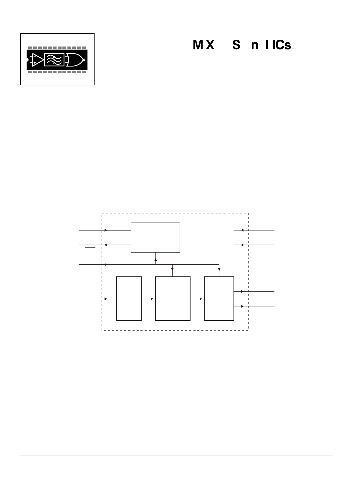
DETECT2
DETECT1
SLICER
SIGIN
XTAL/
CLOCK
SIGNAL
ANALYZER
CONTROL
LOGIC
XTAL/ CLOCK
OSCILLATOR
V
SS
V
DD
XTAL
ENABLE
The MX633 is a low cost, low power device that uses signal processing techniques to detect audible tone signals such as
Dial, Ringing, Busy and other conditions found when placing a call throughout the world’s telecom systems. Detection of
these call progress stages is essential to the proper operation of automatic calling products.
The MX633 adds new features to Call Progress monitoring. It detects and indicates the ‘U.S. Busy’ tones, reducing the
need to measure ‘tone cadence’ to identify ‘U.S. Busy’. It also detects and indicates voice and other signals from Call
Progress tones, reducing voice-falsing and adding voice-answer as a connection prompt.
The MX633 may be used with a 3.0V to a 5.5V supply and is available in the following package styles: 8-pin PDIP
(MX633P) and 16-pin SOIC (MX633DW).
Page 2

Call Progress Tone Detector 2 MX633 - PRELIMINARY INFORMATION
© 1997 MX•COM Inc. www.mxcom.com Tele: 800 638-5577 910 744-5050 Fax: 910 744-5054 Doc. # 20480135.003
4800 Bethania Station Road, Winston-Salem, NC 27105-1201 USA All trademarks and service marks are held by their respective companies.
CONTENTS
Section...............................................................................................................................................Page
1. Block Diagram.................................................................................................................................. 3
2. Signal List......................................................................................................................................... 4
3. External Components...................................................................................................................... 5
4. General Description......................................................................................................................... 6
4.1 Glossary.................................................................................................................................................... 6
4.2 Overall Function Description..................................................................................................................... 6
4.3 Block Diagram Description (Reference Figure 1)......................................................................................6
4.3.1 Slicer..................................................................................................................................................................6
4.3.2 Signal Analyzer..................................................................................................................................................6
4.3.3 Control Logic......................................................................................................................................................7
4.3.4 Xtal/Clock Oscillator...........................................................................................................................................7
4.4 Decode Output Truth Table.......................................................................................................................7
5. Performance Specification.............................................................................................................. 7
5.1 Electrical Performance.............................................................................................................................. 7
5.1.1 Absolute Maximum Ratings...............................................................................................................................7
5.1.2 Operating Limits.................................................................................................................................................8
5.1.3 Operating Characteristics ..................................................................................................................................8
5.1.4 Timing................................................................................................................................................................9
5.2 Packaging ................................................................................................................................................11
MX•COM, Inc. reserves the right to change specifications at any time and without notice
Page 3
Call Progress Tone Detector 3 MX633 - PRELIMINARY INFORMATION
© 1997 MX•COM Inc. www.mxcom.com Tele: 800 638-5577 910 744-5050 Fax: 910 744-5054 Doc. # 20480135.003
4800 Bethania Station Road, Winston-Salem, NC 27105-1201 USA All trademarks and service marks are held by their respective companies.
1. Block Diagram
DETECT2
DETECT1
SLICER
SIGIN
XTAL/
CLOCK
SIGNAL
ANALYZER
CONTROL
LOGIC
C1
C4
R1
X1
C2
C3
XTAL / CLOCK
OSCILLA TOR
V
SS
V
DD
XTAL
ENABLE
Figure 1: Block Diagram
Page 4
Call Progress Tone Detector 4 MX633 - PRELIMINARY INFORMATION
© 1997 MX•COM Inc. www.mxcom.com Tele: 800 638-5577 910 744-5050 Fax: 910 744-5054 Doc. # 20480135.003
4800 Bethania Station Road, Winston-Salem, NC 27105-1201 USA All trademarks and service marks are held by their respective companies.
2. Signal List
Package /
Pin No.
Signal Type Description
PDW
1 2 XTAL/CLOCK input Input to the on-chip oscillator, for external Xtal circuit or clock
23
XTAL
output Output of the on-chip oscillator inverted
3 5 ENABLE input A logic 1 applied to this input enables the decoder and detection outputs. A
logic 0 pulse of at least 1µs applied to this input resets the decoder circuits
and forces both DETECT1 and DETECT2 outputs to a logic 0.
4 7 DETECT1 output When a Call Progress signal is detected, DETECT1 output state changes to a
logic 1
5 10 SIGIN input Signal input. Signals to this pin should be ac coupled. The dc bias of this pin
is set internally.
612 V
SS
power Negative supply
7 13 DETECT2 output Output used in conjunction with DETECT1.
When a Call Progress High Band signal is detected and DETECT1 output
state is a logic 1, then DETECT2 output state changes to a logic 1.
When a Non Call Progress signal is detected and DETECT1 output state is a
logic 0, then DETECT2 output state changes to a logic 0.
815 V
DD
power Positive supply. This pin should be bypassed to V
SS
by a capacitor mounted
close to the device pins.
Table 1: Signal List
Page 5

Call Progress Tone Detector 5 MX633 - PRELIMINARY INFORMATION
© 1997 MX•COM Inc. www.mxcom.com Tele: 800 638-5577 910 744-5050 Fax: 910 744-5054 Doc. # 20480135.003
4800 Bethania Station Road, Winston-Salem, NC 27105-1201 USA All trademarks and service marks are held by their respective companies.
3. External Components
XTAL/
CLOCK
C1
C4
R1
X1
C2
8
7
2
3
4
5
6
DETECT1
MX633P
ENABLE
SIGIN
DETECT2
V
DD
V
SS
C3
1
XTAL
Figure 2: Recommended External Components
R1
1 M
Ω±
10%
C1 33pF
±
20%
C2 33pF
±
20%
C3 560pF at 3.3V
DD
1nF at 5.0V
DD
±
20%
C4 1.0µF
±
20%
X1 Note 1 3.579545MHz refer to sec.5.1
Table 2: Recommended External Components
Notes:
1. For best results, a crystal oscillator design should drive the clock inverter input with signal levels of at least 40% of
V
DD
, peak to peak. Tuning fork crystals generally cannot meet this requirement. To obtain crystal oscillator design
assistance, consult your crystal manufacturer.
Page 6

Call Progress Tone Detector 6 MX633 - PRELIMINARY INFORMATION
© 1997 MX•COM Inc. www.mxcom.com Tele: 800 638-5577 910 744-5050 Fax: 910 744-5054 Doc. # 20480135.003
4800 Bethania Station Road, Winston-Salem, NC 27105-1201 USA All trademarks and service marks are held by their respective companies.
4. General Description
The following Glossary and Decode Truth Table (found in section 4.4), describe the MX633 decoding features and
functions.
4.1 Glossary
Call Progress Tones: The single and dual frequency tones in the range 350Hz to 620Hz specified widely for call
progress signaling.
Call Progress Band: The nominal range 340Hz to 650Hz within which the MX633 will detect Call Progress tones. The
detection algorithm requires that the tones have the characteristics typical of Call Progress Tones.
Call Progress Low Band: The nominal range 340Hz to 490Hz. The MX633 will detect single or dual tones falling
entirely within this range as Call Progress Low Band tones.
Call Progress High Band: The nominal range 600Hz to 650Hz. Single tones in this range, or dual tones
(e.g. 480 + 620Hz), having a material frequency component within this range are detected as Call Progress High Band
tones.
Non Call Progress Signal: A signal falling within the nominal range (a) 200Hz to 800Hz, but NOT within the Call
Progress Band, or (b) within the nominal range 200Hz to 800Hz, but NOT meeting the detection requirements when the
signal falls in the Call Progress Band.
Subject to the duration and other characteristics of such signals, the MX633 will usually interpret this as a Non Call
Progress Signal (e.g. speech or other signal activity).
Minimum Input Signal: The minimum signal level for the specified tone decoding performance.
No Signal: A signal falling outside the nominal range 120Hz to 900Hz or the absence of an input signal. Either will be
detected as a No Signal condition.
Nominal: Subject to dynamic tolerances within the signal analysis process. Absolute values are not material or adverse
to performance.
4.2 Overall Function Description
The MX633 Call Progress Tone Detector uses tone detection methods different from those methods commonly found in
other Call Progress Tone Detectors.
Many Call Progress Tone Detectors use a bandpass filter followed by an energy detector. The filter is usually designed to
pass input signals with a frequency between about 300Hz and 700Hz. Each signal amplitude in this range is checked
against a level threshold. Any signal of acceptable level in this frequency band is classified as a Call Progress tone,
including speech and noise signals. False outputs caused by speech are commonly indicated by such products and
background noise may lead to a stuck detect output.
In contrast, the MX633, uses a stochastic signal processing technique. This technique is based on analysis of both the
frequency and time domains, with signal amplitude forming a small part in the decision process. This analysis includes
checks on whether the signal has a profile that matches international standards for Call Progress tones, speech, noise or
other Non-Call-Progress signals. It also checks for U.S. Busy signal tones.
4.3 Block Diagram Description
(Reference Figure 1)
4.3.1 Slicer
The input signal to the slicer is amplified by a self-biased inverting amplifier. The dc bias of this input is internally set at
V
DD
/2
.
4.3.2 Signal Analyzer
The frequency range, quality and consistency of the input signal is analyzed by this functional block. To be classified as a
call progress signal, the input signal frequencies should lie between 340Hz and 650Hz. The signal to noise ratio must be
16dB or greater and the signal must be consistent over a period of about 140 ms. This decode criteria is continuously
monitored and the assessment updated every 7 ms, reference Figure 3.
The Signal Analyzer samples the call progress signal at 9.3kHz. Care should be taken to avoid high frequency
signals (≥ 8.4kHz) aliasing into the call progress band.
Page 7

Call Progress Tone Detector 7 MX633 - PRELIMINARY INFORMATION
© 1997 MX•COM Inc. www.mxcom.com Tele: 800 638-5577 910 744-5050 Fax: 910 744-5054 Doc. # 20480135.003
4800 Bethania Station Road, Winston-Salem, NC 27105-1201 USA All trademarks and service marks are held by their respective companies.
4.3.3 Control Logic
This block categorizes the nature of the signal into various decode output states and controls the two output pins.
See Table 3.
4.3.4 Xtal/Clock Oscillator
If the on-chip Xtal oscillator is to be used, then external components X1, R1, C1 and C2 are required. If an external clock
source is to be used, then it should be connected to the XTAL/CLOCK input pin and the
XTALpin should be left
unconnected.
4.4
Decode Output Truth Table
DETECT2 DETECT1 CONDITIONS
0 0 No Signal
0 1 Call Progress Low Band:
Will detect 350+440, 400+450, 440+480,400,
425, 440, and 450Hz tones
1 1 Call Progress High Band:
Will detect 480+620, 600 and 620Hz tones
1 0 Non Call Progress signal, e.g. voice activity
Note:
1. DETECT1 responds to the entire range of call progress tones from 340Hz to 650Hz.
Table 3: Decode Output Truth Table
5. Performance Specification
5.1 Electrical Performance
5.1.1 Absolute Maximum Ratings
Exceeding these maximum ratings can result in damage to the device.
General Min. Max. Units
Supply (VDD - VSS)
–
0.3 7.0 V
Voltage on any pin to V
SS
–
0.3 V
DD
+ 0.3 V
Current
V
DD
–
30 30 mA
V
SS
–
30 30 mA
Any other pin
–
20 20 mA
DW / DIP Package
Total Allowable Power Dissipation at T
AMB
= 25°C 800 mW
Derating above 25°C 13 mW/°C above 25°C
Storage Temperature
–
55 125 °C
Operating Temperature
–
40 85 °C
Page 8

Call Progress Tone Detector 8 MX633 - PRELIMINARY INFORMATION
© 1997 MX•COM Inc. www.mxcom.com Tele: 800 638-5577 910 744-5050 Fax: 910 744-5054 Doc. # 20480135.003
4800 Bethania Station Road, Winston-Salem, NC 27105-1201 USA All trademarks and service marks are held by their respective companies.
5.1.2 Operating Limits
Correct operation of the device outside these limits is not implied.
Notes Min. Max. Units
Supply (VDD – VSS) 3.0 5.5 V
Xtal Frequency 3.57 3.59 MHz
5.1.3 Operating Characteristics
For the following conditions unless otherwise specified:
Xtal Frequency = 3.579545MHz, S/N = 16 dB, Noise Bandwidth = 5 kHz,
V
DD
= 3.3V to 5.0V, VSS = 0V, T
AMB
= 25°C, 0dB = 775mV
RMS
.
Notes Min. Typ. Max. Units
DC Parameters
Supply Current
IDD (ENABLE = 1) (VDD = 5.0V) 1 0.5 1.0 mA
IDD (ENABLE = 1) (VDD = 3.3V) 1 0.3 0.7 mA
Enable Input
Input Logic 1 Level 2 80% V
DD
Input Logic 0 Level 2 20% V
DD
Input Leakage Current (V
IN
= 0 to VDD)2– 5.0 5.0 µA
Input Capacitance 2 10.0 pF
Detect Output
Output Logic 1 Level (lOH = 120µA) 3 90% V
DD
Output Logic 0 Level (l
OL
= 360µA) 3 10% V
DD
AC Parameters
SIGIN pin
Input Impedance (from 100Hz to 2kHz at 5.0V) 4 350
k
Ω
Input Signal Level 5
–
40 dB
Input Signal Dynamic Range 5 40 dB
Signal to Noise Ratio 16 dB
Xtal/Clock Oscillator
'High' Input Pulse Width 6 40 ns
'Low' Input Pulse Width 6 40 ns
Input Impedance (at 100Hz) 10
M
Ω
Gain (input = 1mV
RMS
at 100Hz) 20 dB
Operating Characteristics Notes:
1. Not including any current drawn from the device pins by external circuitry.
2. ENABLE pin.
3. DETECT1 and DETECT2 pins.
4. Small signal impedance over the frequency range 100Hz to 2000Hz and at 5.0V
5. The input level is not critical as the detector uses a stochastic algorithm.
6. Timing for an external input to the XTAL/CLOCK pin.
Page 9

Call Progress Tone Detector 9 MX633 - PRELIMINARY INFORMATION
© 1997 MX•COM Inc. www.mxcom.com Tele: 800 638-5577 910 744-5050 Fax: 910 744-5054 Doc. # 20480135.003
4800 Bethania Station Road, Winston-Salem, NC 27105-1201 USA All trademarks and service marks are held by their respective companies.
5.1.4 Timing
For the following conditions unless otherwise specified:
Xtal Frequency = 3.579545MHz, V
DD
= 3.3V to 5.0V, T
AMB
=25°C, S/N = 20dB
Timing (ref. Figures 3, 4, 5 and 6) Notes Min. Typ. Max. Units
t
I
Call Progress Burst Length Ignored 70 ms
t
L
Burst Length Detected 145 ms
t
GI
Call Progress Tone Gap Length Ignored 1 20 ms
t
GD
Call Progress Tone Gap Length Detected 1 40 ms
t
RP
Call Progress Tone Response Time 2 145 ms
t
DRP
Call Progress Tone De-response Time 145 ms
t
GDR
Gap Detected Recorded 3 6 ms
t
NG
Non Call Progress Signal Gap Length Ignored 4 80 ms
t
NRP
Non Call Progress Signal Response Time 145 ms
t
NDRP
Non Call Progress Signal De-response Time 80 ms
t
CH
State Change 0 ms
t
V
DETECT1 and DETECT2 Response Time 5 145 ms
Timing Notes:
1. Only applies to bursts of the same frequency.
2. For dual tones in 16dB SNR the Response Time may be longer.
3. To acknowledge a short tone gap ≥ 40 ms, No Signal is indicated for a minimum of 6ms.
4. If the gap > 90 ms, a No Signal state will be decoded.
5. Time between a stable XTAL/CLK and a valid DETECT1 and DETECT2 state when ENABLE is high.
No Signal
SIGIN
DETECT1
Call Prog r e ss
Low Band
Call Prog r e ss
High Band
Call Prog r e ss
High Band
Call Prog r e ss
High Band
DETECT2
t
I
t
L
t
GD
t
RP
t
DRP
t
GI
t
GDR
ENABLE
t
DRP
t
RP
t
RP
Figure 3: Timing Diagram: Call Progress Tone (s)
Page 10

Call Progress Tone Detector 10 MX633 - PRELIMINARY INFORMATION
© 1997 MX•COM Inc. www.mxcom.com Tele: 800 638-5577 910 744-5050 Fax: 910 744-5054 Doc. # 20480135.003
4800 Bethania Station Road, Winston-Salem, NC 27105-1201 USA All trademarks and service marks are held by their respective companies.
SIGIN
DETECT1
No Signal
Non Call
Progress Signal
Non Call
Progress Signal
DETECT2
t
I
t
L
t
NRP
t
NDRP
t
NG
0 LEVEL
ENABLE
Figure 4 : Timing Diagram: Non Call Progress Signal
SIGIN
DETECT1
No Signal
Call Prog r e ss
Low or High Band
Call Prog r e ss
Low or High Band
Non Call
Progress Signal
DETECT2
t
RP
t
CH
t
RP
t
NRP
ENABLE
Figure 5 : Timing Diagram: Call Progress Tone (s) to Non Call Progress Signal
DETECT 1
DETECT 2
t
V
t = the time at which XTAL/CLOCK becomes stable
S
indeterminate signal
valid signal
XTAL/CLOCK
Figure 6: Timing Diagram: DETECT 1 and DETECT 2 Response Time when ENABLE is high
Page 11

Call Progress Tone Detector 11 MX633 - PRELIMINARY INFORMATION
© 1997 MX•COM Inc. www.mxcom.com Tele: 800 638-5577 910 744-5050 Fax: 910 744-5054 Doc. # 20480135.003
4800 Bethania Station Road, Winston-Salem, NC 27105-1201 USA All trademarks and service marks are held by their respective companies.
5.2 Packaging
A
B
PIN1
MJ1
Y
E1
T
E
K
K1
P
H
C
J
F
L
A
B
C
E
E1
F
H
TYP. MAX.MIN.
DIM.
J
J1
P
Y
T
K1
K
L
M
0.200 (5.06)
0.260 (6.60)
0.390 (9.87).
7°
0.150 (3.81)
0.400 (10.16)
0.145 (3.68)
0.100 (2.54)
0.121 (3.07)
0.020 (0.51)
0.300 (7.62)
0.290 (7.37) 0.325 (8.22)
0.30 (7.62)
0.040 (1.01)
0.008 (0.20) 0.015 (0.38)
0.015 (0.38) 0.023 (0.58)
0.045 (1.14) 0.065 (1.65)
0.060 (1.52)
0.060 (1.52)
0.346 (8.790)
0.240 (6.10)
NOTE: Alldimensions in inches(mm.)
Angles are in degrees
Pac kageTolerances
0.015 (0.38)
0.033 (0.84)
Figure 7 : 8-pin PDIP Mechanical Outline:
Order as part no. MX633P
PIN 1
A
B
ALTERNATIVE
PIN
LOCA TION
MARKING
X
P
J
Y
C
K
H
E
L
T
W
Z
NOTE: Alldimensions in inches(mm.)
Angles are in degrees
Packa geTolerances
A
B
C
E
H
TYP.
MAX.MIN.
DIM.
J
P
X
W
T
Y
K
L
0.105 (2.67)0.093 (2.36)
0.419 (10.64)
45°
7°
0° 10°
0.050 (1.27)
0.041 (1.04)
0.413 (10.49)
0.299 (7.59)
0.050 (1.27)
0.016 (0.41)
0.390 (9.90)
0.020 (0.51)0.003 (0.08)
0.009 (0.23) 0.0125 (0.32)
0.013 (0.33) 0.020 (0.51)
0.395 (10.03)
0.286 (7.26)
Z
5°
5°
Figure 8 : 16-pin SOIC Mechanical Outline:
Order as part no. MX633DW
 Loading...