

Page 1
DATA BULLETIN
MX623
PRELIMINARY INFORMATION
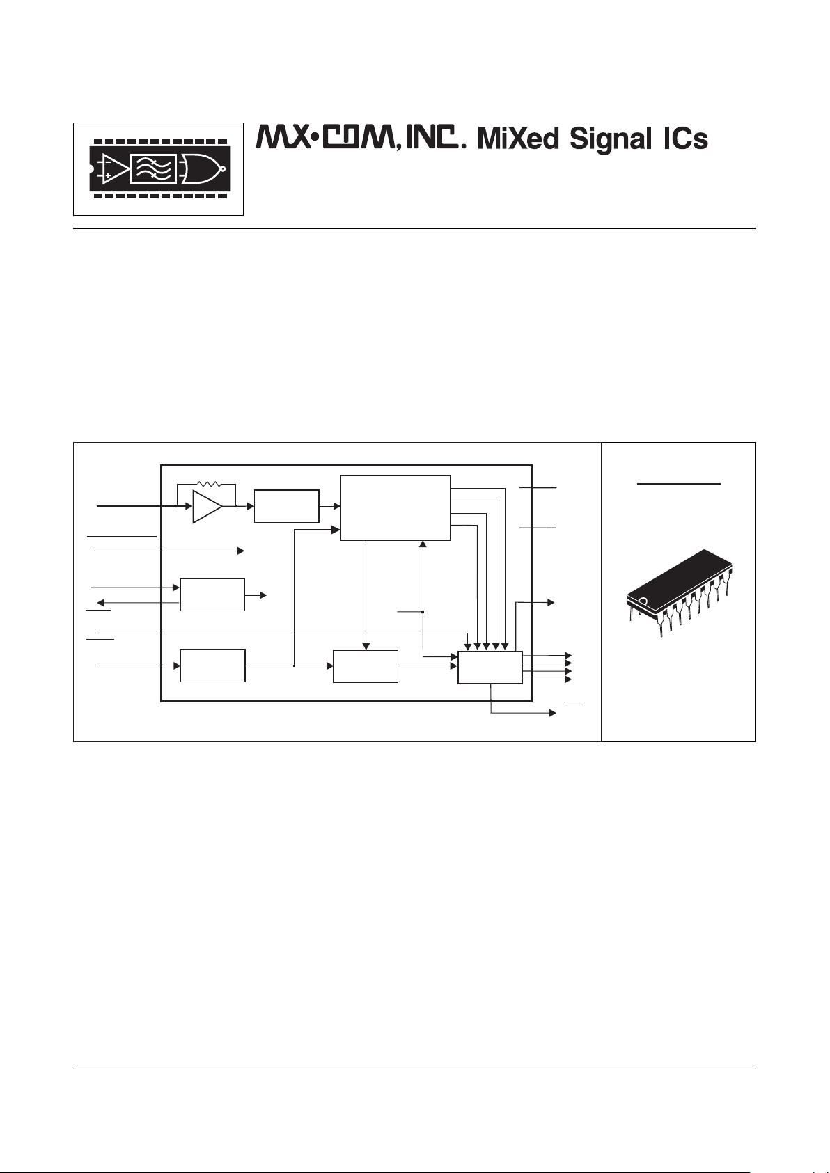
The MX623 is a low-power decoding integrated circuit that measures the frequency of telephone system call progress
tones.
With progress signals input from the telephone line, this single-chip product is programmed to recognize up to thirteen
of the World's most commonly used call-progress frequencies, analyze signal quality, and present the measured result
as a 4-bit parallel data word at the tri-state Data Output.
Using the parallel information from the MX623, the host system, can recognize such call progress information as: ‘Dial’,
‘Busy’, ‘Number Unobtainable’, ‘Ringing’ and Fax/Modem system signals.
This information can then be used in simple or complex applications to control telephone operations. The data output
will require a software format that can analyze the frequency information from the MX623.
Requiring only a single 3.0
[MIN]
volt power supply, the MX623 may be line-powered and will operate under simple logic
or system µProcessor control using the 'Data-Change, 'Hold' and 'Chip-Select' functions.
The MX623, whose small size and low power consumption makes it ideal for remote applications, requires a
3.579545MHz telephone system clock or Xtal input, is available in a 16-pin PDIP.
AVAILABLE
PACKAGES
MX623P
16-pin PDIP
XTAL/CLOCK
OSCILLATOR
SIGNAL IN
XTAL/CLOCK
Clocks
Clocks
DATA
CHANGE
DATA
OUTPUTS
Q0
Q1
Q2
Q3
IRQ
V
DD
V
SS
CONTROL
CIRCUITRY
TIMER
CHIP SELECT
HOLD
PURS
DIGITAL
FIL TER
OUTPUT
LATCHES
LIMITER
XTAL
MEASUREMENT
AND
DECODE
• MX•COM MiXed Signal CMOS
• Custom Tone Decoder (13 Call-Progress
Frequencies Recognized)
• Operates to a 3.579545MHz Telephone System
Clock
• Operates Under Simple Logic or µProcessor
System Control
• Measures Call Progress Tone Frequencies
(‘Busy’, ‘Dial’, ‘Fax-Tone’ etc.)
• Telephone, PABX, Fax and Dial-Up Modem
Applications
• Low-Power Requirement (600µA at 3.3 Volts
TYP
)
for Line-Powered Applications
Line-Powered Call Progress
Tone Detector
© 1997 MX•COM Inc. www.mxcom.com Tele: 800 638-5577 910 744-5050 Fax: 910 744-5054 Doc. # 20480091.003
4800 Bethania Station Road, Winston-Salem, NC 27105-1201 USA All trademarks and service marks are held by their respective companies.
Page 2
© 1997 MX•COM Inc. www.mxcom.com Tele: 800 638-5577 910 744-5050 Fax: 910 744-5054 Doc. # 20480091.003
4800 Bethania Station Road, Winston-Salem, NC 27105-1201 USA All trademarks and service marks are held by their respective companies.
Line- Powered Call Progress Detector 2 MX623 Preliminary Information
Q3:
Q2:
Q1:
Q0:
VDD: Positive supply rail. A minimum supply voltage of 3.0 volts is required. Levels and voltages
within this decoder are dependent upon this supply.
Signal In: The composite audio input. Signals to this pin should be a.c. coupled. The d.c. bias of
the limiter section is set internally; this pin should not be loaded with any other circuitry.
No internal connection. Leave open circuit.
Xtal: The output of the on-chip clock oscillator inverter.
No internal connection. Leave open circuit.
Xtal/Clock: The input to the clock oscillator inverter. A 3.579545MHz Xtal or externally derived
clock should be connected here (see Figure 2).
VSS: Negative supply rail (GND).
Hold: An input to control the Output Latch condition; employed in combination with the Data
Change output to facilitate, if required, Interrupt and/or handshake operations with a µProcessor.
With Hold placed “Low”, with a tone input, the Data Change output will be held “High” at the next
data change, and the current output code is locked in the Output Latches regardless of any
changes to the input signal. The output code remains as held until this input is returned “High”
(see Figure 3). While this input is “High” the output data, Q0 - Q3, cycles normally with the input
audio. This pin has an internal 1.0MΩ pullup resistor.
PURS: Power-Up ReSet. To reset internal circuitry at power-up; a logic “1” level is required at this
pin for a duration of at least 2.5ms after the Xtal/Clock input and full VDD levels are applied. The
component configuration shown in Figure 2 is recommended; for slow-rising power supplies the
time constant of components should be increased accordingly.
IRQ: Interrupt Request. An output for µProcessor operation; normally “High” this output is latched
“Low” when an internal data change occurs if the Chip Select input is “High”. This output is reset
(“High”) the when Chip Select line is taken “Low”. To permit “wire-OR” connection with other
peripherals, this output has a low-impedance when “Low” and a high-impedance when “High”.
CS: Chip Select- A controlling function. When held “High” the Data Outputs Q0, Q1, Q2 and Q3
and the Data Change output are disabled. When taken “Low” the Data Outputs Q0, Q1, Q2 and
Q3 and the Data Change output are enabled; the Interrupt Request (IRQ) is reset (“High”) when
CS is taken “Low”. See Figures 3 and 4.
Data Change: A positive-going pulse is generated at this output when the data changes (Tone or
NOTONE). New tone-data is presented to the Q0, Q1, Q2 and Q3 Data Outputs if the Hold input is
set “High”. This is a tri-state output.
1
2
3
4
5
6
7
8
9
10
11
12
13
14
15
16
Data Outputs: A 4-bit parallel data word, forming a HEX character representing the decoded
tone frequency. This word is output after a successful decode. Table 1 details the Hex
character output codes for the relevant decoded tone frequencies. Upon power-up this output
is set to ‘EH’, but no Data Change pulse generated. These are tri-state outputs.
Pin Function
Page 3

© 1997 MX•COM Inc. www.mxcom.com Tele: 800 638-5577 910 744-5050 Fax: 910 744-5054 Doc. # 20480091.003
4800 Bethania Station Road, Winston-Salem, NC 27105-1201 USA All trademarks and service marks are held by their respective companies.
Line- Powered Call Progress Detector 3 MX623 Preliminary Information
Application Information
Figure 2 - Recommended External Components
Band Edges (Hz) Nominal
Hex Output Code Lower Upper Center
Character Q3 Q2 Q1 Q0 Edge Edge Freq.
0 0000 364 386
375
1 0001 488 520
500
2 0010 520 580
550
3 0011 580 618
600
4 0100 386 412
400
5 0101 412 436
425
6 0110 436 463
450
7 0111 463 487
475
8 1000 900 1008
950
9 1001 1273 1325
1300
A 1010 1350 1455
1400
B 1011 1750 1855
1800
C 1100 2062 2140
2100
D 1101 frequency not guaranteed
E 1110 frequency not guaranteed
F 1111 NOTONE
Table 1 - Tone Decode Frequencies
Timing Information
With CS Low - Figure 3
After initial power-up and the Hold input inactive (High),
as frequencies are input, with the Data Change output
as an active (High) indicator, the data is presented at
the Data Outputs.
If/when the Hold input is placed active (Low), the data
at the Data Outputs is frozen and the Data Change
output held High at its next active excursion -until the
Hold input is returned High.
With the Hold input held High - Figure 4
As frequencies are input a correct decode will produce
an active (Low) interrupt level.
This interrupt (IRQ) is serviced and reset by an active
(Low) CS input.
Note the ‘valid data’ period at the Data Outputs.
Component Value
R
1
1.0MΩ
R
2
1.0MΩ
C
1
.047µF
C
2
.0047µF
Component Value
C
3
33.0pF
C
4
33.0pF
C
5
1.0µF
X
1
3.579545MHz
Tolerances R = ±10%, C = ±20%
V
DD
V
DD
V
DD
C
1
R
1
C
4
X
1
R
2
C
3
C
2
V
SS
1
2
3
4
5
6
7
8
16
15
14
13
12
11
10
9
XTAL/CLOCK
PURS
DATA CHANGE
SIGNAL IN
COMPOSITE SIGNAL IN
A HEX Code
Output representing
the decoded tone
frequency --
See Table 1
DAT A OUTPUTS
Q3
Q0
Q1
Q2
C
5
XTAL
HOLD
IRQ
CS
MX623P
Page 4

© 1997 MX•COM Inc. www.mxcom.com Tele: 800 638-5577 910 744-5050 Fax: 910 744-5054 Doc. # 20480091.003
4800 Bethania Station Road, Winston-Salem, NC 27105-1201 USA All trademarks and service marks are held by their respective companies.
Line- Powered Call Progress Detector 4 MX623 Preliminary Information
Application Information - Decoder Timing
V
DD
SIGNAL IN
OUTPUTS
Q0 - Q3
DATA OUT Q0 - Q3
(INTERNAL)
DATA CHANGE
IRQ
CS
NOTONE
TRI-STATE TRI-STATE
VALID DATA
(READ D ATA)
VALID DATA
(READ D ATA)
T one 1
RIRQ
t
IR
t
ACS
t
HIZ
t
EF
1
t
PURS
PURS
Figure 4 - Timing with the HOLD Input Held “High”; CS and IRQ are used
Figure 3 - Timing with the Chip Select Input Held “Low”; CS and IRQ are not used
t
RESP
t
DE
V
DD
NOTONE
NOTONE
OUTPUTS
Q0 to Q3
DATA CHANGE
SIGNAL IN
T one 1 T one 2 T one 3 T one 'N'
'N'
HOLD
t
PURS
PURS
t
NT
t
DC
HOLD
t
NORM
t
PUL
t
Page 5

© 1997 MX•COM Inc. www.mxcom.com Tele: 800 638-5577 910 744-5050 Fax: 910 744-5054 Doc. # 20480091.003
4800 Bethania Station Road, Winston-Salem, NC 27105-1201 USA All trademarks and service marks are held by their respective companies.
Line- Powered Call Progress Detector 5 MX623 Preliminary Information
Characteristics See Note Min. Typ. Max. Unit
Static Values
Supply Current - 0.6 1.0 mA
Input Logic “1” 0.7 - - %V
DD
Input Logic “0” - - 0.3 %V
DD
Output Logic “1” 0.8 - - %V
DD
Output Logic “0” - - 0.2 %V
DD
Impedance
CS and PURS Input 10.0 - - MΩ
Hold Input 1 0.5 - - MΩ
Signal Input 0.1 - - MΩ
IRQ Output (logic “1”) - 30.0 100 kΩ
IRQ Output (logic “0”) - 17 5 500 Ω
Q0 - Q3 & Data-Change Outputs (logic “1”) - 0.7 2.0 kΩ
Q0 - Q3 & Data-Change Outputs (logic “0”) - 175 500 Ω
Q0 - Q3 & Data-Change Outputs (high Z) 1.0 - - MΩ
Dynamic Values
Signal Input Range 2, 5 35.0 1,166 mVrms
Decode Bandedge Tolerance 3 -1.0 - 1.0 %
Xtal Inverter
Voltage Gain 20.0 - - V/V
Input Impedance 10.0 - - MΩ
Output Impedance - - 160 kΩ
Decoder Timing -
Figures 3 and 4
Power Up Reset Time t
PURS
2.5 - - ms
Data 'E' Time t
DE
31.0 - - ms
NOTONE to Tone Response Time t
RESP
4 - 27.0 50.0 ms
Specifications
Absolute Maximum Ratings
Exceeding the maximum rating can result in device
damage. Operation of the device outside the operating
limits is not implied.
Supply voltage -0.3 to 7.0V
Input voltage at any pin
(ref V
SS
= 0V) -0.3 to (V
DD
+ 0.3V)
Sink/source current
(supply pins) +/- 30mA
(other pins) +/- 20mA
Total device dissipation
@ T
AMB
25°C 800mW Max.
Derating 10mW/°C
Storage temperature range -40°C to +85°C
Operating Limits
Min. Max. Unit
Supply Voltage (VDD) 3.0 5.5 V
at 25°C
Operating Temperature -40 +85 °C
All device characteristics are measured under the
following conditions unless otherwise specified:
V
DD
= 3.3V
T
OP
= 25 °C
Audio Level 0dB ref: = 775mVrms
Xtal/Clock Frequency = 3.579545MHz
Page 6

© 1997 MX•COM Inc. www.mxcom.com Tele: 800 638-5577 910 744-5050 Fax: 910 744-5054 Doc. # 20480091.003
4800 Bethania Station Road, Winston-Salem, NC 27105-1201 USA All trademarks and service marks are held by their respective companies.
Line- Powered Call Progress Detector 6 MX623 Preliminary Information
Tone to NOTONE Response Time t
NT
4 - - 60.0 ms
Data to Data-Change Pulse Time t
DC
0.625 - 1.15 ms
Data-Change Pulse Width t
PUL
- 1.25 - ms
Hold to Data-Change Rise Time t
HOLD
63.0 - - µs
HOLD to Data-Change Fall Time t
NORM
- - 150 µs
IRQ Tone Response Time t
RIRQ
- 29.0 52.0 ms
IRQ Reset Time t
IR
- - 250 ns
Data Access Time t
ACS
- - 250 ns
CS High to Output Tri-State Time t
HIZ
- - 100 ns
Notes
1. This pin has an on-chip 1.0MΩ pullup resistor.
2. An a.c. coupled sine or squarewave.
3. See Table 1, Tone Decode Frequencies.
4. Delay between the change of input (Tone/NOTONE) and the change at the Q0 - Q3 outputs.
5. The signal input maximum value is determined by the formula VDD/2.83.
Characteristics See Note Min. Typ. Max. Unit
NOTE: All dimen s io n s in inches (mm.)
Angles are in degrees
Packa geTolerances
A
B
C
E
E1
H
TYP. MAX.MIN.DIM.
J
J1
P
Y
T
K
L
0.220 (5.59)
0.555 (14.04)
0.670 (17.02)
7°
0.160 (4.05)
1.270 (32.26)
0.151 (3.84)
0.100 (2.54)
0.121 (3.07)
0.600 (15.24)
0.590 (14.99) 0.625 (15.88)
0.015 (0.38) 0.045 (1.14)
0.008 (0.20) 0.015 (0.38)
0.015 (0.38) 0.023 (0.58)
0.040 (1.02) 0.065 (1.65)
0.066 (1.67) 0.074 (1.88)
1.200 (30.48)
0.500 (12.70)
H
K
L
J1J1
JJ
PP
CC
BB
AA
PIN1PIN1
TT
EE
E1E1
Y
Figure 5: 16-pin PDIP Mechanical Outline:
order as part no. MX623P
 Loading...