

Page 1
COMMUNICATION ICs
DATA BULLETIN
MX619
Delta Modulation Codec
meets EUROCOM D1-IA8
2000 MX-COM, Inc. www.mxcom.co m Tel: 800 638 5577 336 744 5050 Fax: 336 744 5054 Doc. # 20480189.002
4800 Bethania Station Road, Winston-Salem, NC 27105-1201 USA All Trademarks and service marks are held by their respective companies.
Features Applications
•
Meets EUROCOM D1-IA8
•
Single Chip Full Duplex CVSD CODEC
•
On-chip Input and Output Filters
•
Programmable Sampling Clocks
•
3- or 4-bit Companding Algorithm
•
Powersave Capabilities
•
Low Power, 5.0V Operation
•
Military Communications
•
Multiplexers, Switches, & Phones
➤
➤
➤
➤
➤
➤
➤
➤
➤
➤
➤
➤➤
➤
➤
➤
➤
➤➤
➤
➤
➤
➤
➤
➤
➤
➤
➤
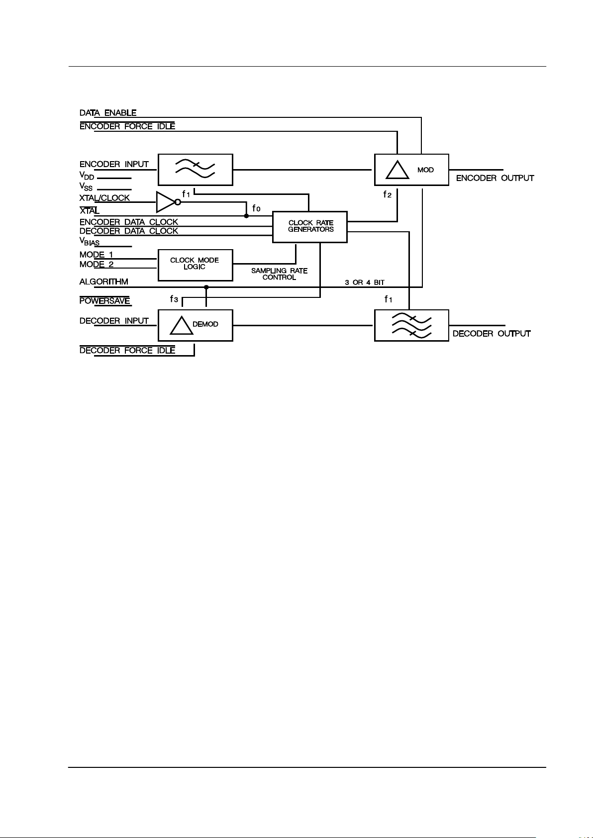
The MX619 is a Continuously Variable Slope Delta Modulation (CVSD) Codec designed for use in military
communications systems. This device is suitable for applications in military delta multiplexers, switches, and
phones. The MX619 is designed to meet EUROCOM D1-IA8 specifications.
Encoder input and decoder output filters are incorporated on-chip. Sampling clock rates can be programmed
to 16, 32, or 64kbps from an internal clock generator or externally injected in the 8 to 64kbps range. The
sampling clock frequency is output for the synchronization of external circuits.
The encoder has an enable function for use in multiplexer applications. Encoder and Decoder forced idle
capabilities are provided forcing 10101010…pattern in encode and a V
DD
/2 bias in decode. The companding
circuit may be operated with an externally selectable 3- or 4-bit algorithm. The device may be placed in
standby mode by selecting Powersave. A reference 1.024MHz oscillator uses an external clock or crystal.
The MX619 operates with a supply voltage of 5.0V and is available in the following packages: 24-pin PLCC
(MX619LH), 22-pin CERDIP (MX619J), and 22-pin PDIP (MX619P).
Page 2

Delta Modulation CODEC 2 MX619
2000 MX-COM, Inc. www.mxcom.com Tel: 800 638 5577 336 744 5050 Fax: 336 744 5054 Doc. # 20480189.002
4800 Bethania Station Road, Winston-Salem, NC 27105-1201 USA All Trademarks and service marks are held by their respective companies.
CONTENTS
Section Page
1 Block Diagram................................................................................................................3
2 Signal List.......................................................................................................................4
3 External Components....................................................................................................6
4 General Description.......................................................................................................6
5 Application .....................................................................................................................7
5.1 CODEC Integration.............................................................................................................. 7
5.2 Digital to Analog Performance............................................................................................. 7
6 Performance Specification..........................................................................................11
6.1 Electrical Performance...................................................................................................... 11
6.1.1 Absolute Maximum Ratings..................................................................................................11
6.1.2 Operating Limits...................................................................................................................11
6.1.3 Operating Characteristics.....................................................................................................12
6.1.4 TIMING.................................................................................................................................13
6.2 Packaging.......................................................................................................................... 14
MX-COM, Inc. reserves the right to change specifications at any time and without notice.
Page 3
Delta Modulation CODEC 3 MX619
2000 MX-COM, Inc. www.mxcom.com Tel: 800 638 5577 336 744 5050 Fax: 336 744 5054 Doc. # 20480189.002
4800 Bethania Station Road, Winston-Salem, NC 27105-1201 USA All Trademarks and service marks are held by their respective companies.
1 Block Diagram
➤
➤
➤
➤
➤
➤
➤
➤
➤
➤
➤
➤➤
➤
➤
➤
➤
➤➤
➤
➤
➤
➤
➤
➤
➤
➤
➤
Figure 1: Block Diagram
Page 4
Delta Modulation CODEC 4 MX619
2000 MX-COM, Inc. www.mxcom.com Tel: 800 638 5577 336 744 5050 Fax: 336 744 5054 Doc. # 20480189.002
4800 Bethania Station Road, Winston-Salem, NC 27105-1201 USA All Trademarks and service marks are held by their respective companies.
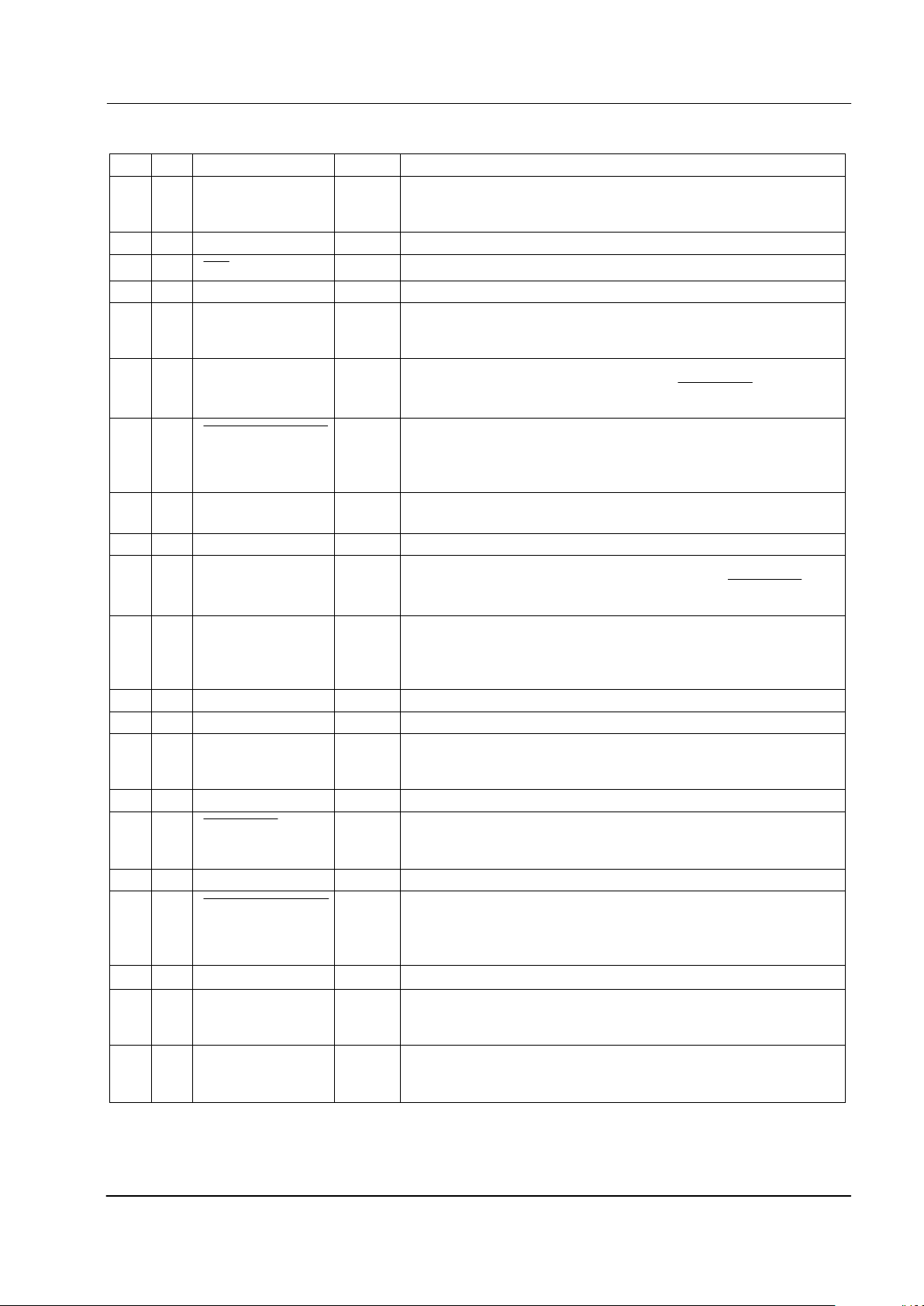
2 Signal List
J/P LH Name Signal Description
1 1 Xtal/Clock input Input to the clock oscillator inverter. A 1.024MHz Xtal input or
externally derived clock is injected here. See Clock Mode pins
and Figure 2.
2 N/C No Connection
2 3
Xtal
output The 1.024 MHz output of the clock oscillator inverter.
3 4 N/C No Connection
4 5 Encoder Data
Clock
input/
output
A logic I/O port. External encode clock input or internal data
clock output. Clock frequency is dependent upon Clock Mode 1,
2 inputs and Xtal frequency (see Clock Mode pins).
5 6 Encoder Output output The encoder digital output. This is a three-state output whose
condition is set by the Data Enable and
Powersave inputs. See
Table 2.
6 7
Idle Force Encoder
When this pin is at a logical “0” the encoder is forced to an idle
state and the encoder digital output is 0101, a perfect idle
pattern. When this pin is a logical “1” the encoder encodes as
normal. Internal 1MΩ pullup.
7 8 Data Enable input Data is made available at the encoder output pin by control of
this input. See Encoder Output pin. Internal 1 MΩ pullup.
8 9 N/C No Connection
9 10 V
BIAS
Normally at VDD/2 bias, this pin should be externally decoupled
by capacitor C4. Internally pulled to V
SS
when “
Powersave
” is
a logical “0”.
10 11 Encoder Input input The analog signal input. Internally biased at VDD/2, this input
requires an external coupling capacitor. The source impedance
should be less than 100Ω. Output channel noise levels will
improve with an even lower source impedance. See Figure 2.
11 12 VSS power Negative Supply
12 13 N/C No Connection
13 14 Decoder Output output The recovered analog signal is output at this pin. It is the
buffered output of a lowpass filter and requires external
components. During “Powersave” this output is open circuit.
14 15 N/C No Connection
15 16
Powersave
A logic “0” at this pin puts most parts of the codec into a
quiescent non-operational state. When at a logical “1”, the
codec operates normally. Internal 1 MΩ pullup.
17 N/C No Connection
16 18
Idle Force Decoder
A logic “0” at this pin gates a 0101... pattern internally to the
decoder so that the Decoder Output goes to V
DD
/2. When this
pin is a logical “1” the decoder operates as normal. Internal
1MΩ pullup.
17 19 Decoder Input
The received digital signal input. Internal 1 MΩ pullup.
18 20 Decoder Data
Clock
input/
output
A logic I/O port. External decode clock input or internal data
clock output, dependent upon clock mode 1,2 inputs. See Clock
Mode pins.
19 21 Algorithm A logic “1” at this pin sets this device for a 3-bit companding
algorithm. A logical “0” sets a 4-bit companding algorithm.
Internal 1 MΩ pullup.
Page 5
Delta Modulation CODEC 5 MX619
2000 MX-COM, Inc. www.mxcom.com Tel: 800 638 5577 336 744 5050 Fax: 336 744 5054 Doc. # 20480189.002
4800 Bethania Station Road, Winston-Salem, NC 27105-1201 USA All Trademarks and service marks are held by their respective companies.
J/P LH Name Signal Description
20 22 Clock Mode 2
21 23 Clock Mode 1
Clock rates refer to f = 1024MHz Xtal/Clock input. During
internal operation the data clock frequencies are available at
the ports for external circuit synchronization. Independent or
common data rate inputs to Encode and Decode data clock
ports may be employed in the External Clocks mode. Internal
1MΩ pullups. See Table 3.
22 24 VDD power Positive Supply. A single 5.0V supply is required.
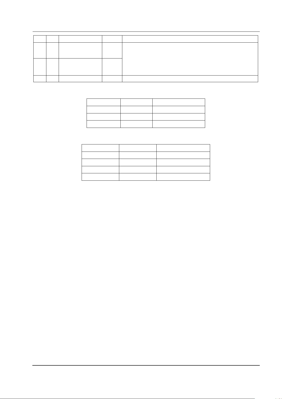
Table 1: Signal List
Data Enable Powersave Encoder Output
1 1 Enable
0 1 High Z (open circuit)
1 0 VSS
Table 2: Encoder Output
Clock Mode 1 Clock Mode 2 Facility
0 0 External Clocks
0 1 Internal, 64kbps = f/16
1 0 Internal, 32kbps = f/32
1 1 Internal, 16kbps = f/64
Table 3: Clock Mode
Page 6

Delta Modulation CODEC 6 MX619
2000 MX-COM, Inc. www.mxcom.com Tel: 800 638 5577 336 744 5050 Fax: 336 744 5054 Doc. # 20480189.002
4800 Bethania Station Road, Winston-Salem, NC 27105-1201 USA All Trademarks and service marks are held by their respective companies.
3 External Components
1
2
3
4
5
6
7
8
9
10
11
22
21
20
19
18
17
16
15
14
13
12
MX619J
XT AL
ENCODER FORCE IDLE
N/C
ENCODER DA TA CLOCK
ENCODER OUTPUT
DAT A ENABLE
N/C
BIAS
ENCODER INPUT
V
SS
XT AL/CLOCK
R1
R2
X1
C2
C1
V
DD
V
DD
C3
C4
C5
CLOCK MODE 1
CLOCK MODE 2
ALGORITHM
DECODER DA TA CLOCK
DECODER INPUT
N/C
DECODER OUTPUT
N/C
DECODER FORCE IDLE
POWERSAVE
Figure 2: Recommended External Components for Typical Application
R1 Note 1
1MΩ
±
10%
C3 Note 4
1.0µF
±
20%
R2 Note 2 Selectable C4 Note 5
1.0µF
±
20%
C1 Note 3 33pF
±
20%
C5 Note 6
1.0µF
±
20%
C2 Note 3 68pF
±
20%
X1 Note 7, 8 1.024MHz
Table 4: Recommended External Components for Typical Application
Notes:
1. Oscillator inverter bias resister.
2. Xtal Drive limiting resistor.
3. Xtal circuit load capacitor.
4. Encoder input coupling capacitor. The drive source impedance to this input should be less than 100Ω.
Output idle channel noise levels will improve with even lower source impedance.
5. Bias decoupling capacitor
6. V
DD
decoupling capacitor
7. A 1.024MHz Xtal/Clock input will yield exactly 16/32/64kbps data clock rates. Xtal circuitry shown is in
accordance with MX-COM’s Xtal Oscillator Application Note.
8. For best results, a crystal oscillator design should drive the clock inverter input with signal levels of at
least 40% of V
DD
, peak to peak. Tuning fork crystals generally cannot meet this requirement. To obtain
crystal oscillator design assistance, please consult you crystal manufacturer.
4 General Description
The MX619 is a Continuously Variable Slope Delta Modulation (CVSD) Codec designed for use in military
communications systems. This device is suitable for applications in military delta multiplexers, switches and
phones. The MX619 is designed to meet EUROCOM D1-IA8 specifications.
Encoder input and decoder output filters are incorporated on-chip. Sampling clock rates can be programmed
to 16, 32, or 64kbps from an internal clock generator or externally injected in the 8 to 64kbps range. The
sampling clock frequency is output for the synchronization of external circuits.
The encoder has an enable function for use in multiplexer applications. Encoder and Decoder forced idle
capabilities are provided forcing 10101010…pattern in encode and a V
DD
/2 bias in decode. The companding
circuit may be operated with an externally selectable 3- or 4-bit algorithm. The device may be placed in
standby mode by selecting Powersave. A reference 1.024MHz oscillator uses an external clock or crystal.
Page 7

Delta Modulation CODEC 7 MX619
2000 MX-COM, Inc. www.mxcom.com Tel: 800 638 5577 336 744 5050 Fax: 336 744 5054 Doc. # 20480189.002
4800 Bethania Station Road, Winston-Salem, NC 27105-1201 USA All Trademarks and service marks are held by their respective companies.
5 Application
Due to the very low levels of a signal idle channel noise specified for military applications, a noisy or badly
regulated power supply could cause instability, putting the overall system performance out of specification.
Adherence to the points listed below will assist in minimizing this problem.
1. Care should be taken in the design and layout of the printed circuit board.
2. All external components (as recommended in Figure 2) should be kept close to the package.
3. Tracks should be kept short, particularly the Encoder Input capacitor and the V
BIAS
capacitor.
4. Xtal/Clock tracks should be kept well away from analog inputs and outputs.
5. Inputs and outputs should be screened whenever possible.
6. A ‘ground plane’ connected to V
SS
will assist in eliminating external pick-up on the input and output pins.
7. It is recommended that the power supply rails have less that 1mV
RMS
of noise allowed.
8. The source impedance to the Encoder Input pin must be less that 100W; output idle channel, noise levels
will improve with even power source impedances.
5.1 CODEC Integration
SYNCHRONOUS CLOCK
AND DA TA SYSTEM
ANALOG
INPUT
INTERFACE
(BALUN &
BUFFER)
ANALOG
OUTPUT
INTERFACE
(BALUN &
BUFFER)
SYSTEM
INPUT
SYSTEM
OUTPUT
MX619 PARAMETERS
MEASURED HERE
MX619 PARAMETERS
MEASURED HERE
REGULATED
POWER SUPPLY
MX619
ENCODER
MX619
DECODER
CLOCK MODE
16/32/64 KB/S
DATA
DATA
CLOCKS
CLOCKS
1.024MHz
1.024MHz
Figure 3: System Configuration using the MX619
5.2 Digital to Analog Performance
Test Sample
Rate
Bit Sequence at Decoder Input MLA
Duty Cycle
Typical
Output
Level
a 16kbps
32kbps
10110100100100101101
1011011010101001001001001001010101101101
0
0
-41.5dBmO
–42.5dBmO
b 16kbps
32kbps
11011001001001001101
1011011010101001001000100100101011011011
0.05
0.05
-25.0dBmO
–25.0dBmO
c 16kbps
32kbps
10110101000100101011
1101101101010010001000100100101011011101
0.1
0.1
-19.0dBmO
-18.5dBmO
d 16kbps
32kbps
11011001000010011011
1101110110010100010000100010011010111011
0.2
0.2
-11.0dBmO
–11.5dBmO
e 16kbps
32kbps
11011010000010010111
111011101100100010000001001001101110111
0.3
0.3
-6.5dBmO
–6.5dBmO
f 16kbps
32kbps
11011010000001001111
1111011101010001000000001000101011101111
0.4
0.4
-3.0dBmO
–3.0dBmO
g 16kbps
32kbps
111010100000001011
1111101110100010000000000100010111011111
0.5
0.5
0dBmO
0dBmO
Table 5: Bit Sequence Test
Page 8

Delta Modulation CODEC 8 MX619
2000 MX-COM, Inc. www.mxcom.com Tel: 800 638 5577 336 744 5050 Fax: 336 744 5054 Doc. # 20480189.002
4800 Bethania Station Road, Winston-Salem, NC 27105-1201 USA All Trademarks and service marks are held by their respective companies.
Figure 4: Gain vs. Input Level (16kbps)
Figure 5: Gain vs. Input Level (32kbps)
Figure 6: S/N vs. Input Level (16kbps)
Page 9

Delta Modulation CODEC 9 MX619
2000 MX-COM, Inc. www.mxcom.com Tel: 800 638 5577 336 744 5050 Fax: 336 744 5054 Doc. # 20480189.002
4800 Bethania Station Road, Winston-Salem, NC 27105-1201 USA All Trademarks and service marks are held by their respective companies.
Figure 7: S/N vs. Input Level (32kbps)
Figure 8: Attenuation distrotion vs. Frequency (16kbps)
Figure 9: S/N vs. Input Frequency (16kbps)
Page 10

Delta Modulation CODEC 10 MX619
2000 MX-COM, Inc. www.mxcom.com Tel: 800 638 5577 336 744 5050 Fax: 336 744 5054 Doc. # 20480189.002
4800 Bethania Station Road, Winston-Salem, NC 27105-1201 USA All Trademarks and service marks are held by their respective companies.
Figure 10: S/N vs. Input Frequency (32kbps)
Figure 11: Principal Integrator Response
➤
➤
➤
➤
➤
➤
Figure 12: Compand Envelope
Page 11

Delta Modulation CODEC 11 MX619
2000 MX-COM, Inc. www.mxcom.com Tel: 800 638 5577 336 744 5050 Fax: 336 744 5054 Doc. # 20480189.002
4800 Bethania Station Road, Winston-Salem, NC 27105-1201 USA All Trademarks and service marks are held by their respective companies.
Figure 13: Attenuation Distortion vs. Frequency (32kbps)
6 Performance Specification
6.1 Electrical Performance
6.1.1 Absolute Maximum Ratings
Exceeding these maximum ratings can result in damage to the device.
Min. Max. Units
Supply (VDD - VSS) -0.3 7.0 V
Voltage on any pin to VSS -0.3 V
DD
+ 0.3 V
Current
VDD -30 30 mA
VSS -30 30 mA
any other pin -20 20 mA
J / P / LH Packages
Total Allowable Power Dissipation at T
AMB
= 25°C - 800 mW
Derating above 25°C - 10 mW/°C above 25°C
Storage Temperature -55 125 °C
Operating Temperature -40 85 °C
6.1.2 Operating Limits
Correct operation of the device outside these limits is not implied.
Min Typ. Max. Units
Supply (VDD - VSS) 4.5 5.0 5.5 V
Operating Temperature -40 85 °C
Xtal Frequency 500 1.024 1500 MHz
Page 12

Delta Modulation CODEC 12 MX619
2000 MX-COM, Inc. www.mxcom.com Tel: 800 638 5577 336 744 5050 Fax: 336 744 5054 Doc. # 20480189.002
4800 Bethania Station Road, Winston-Salem, NC 27105-1201 USA All Trademarks and service marks are held by their respective companies.
6.1.3 Operating Characteristics
For the following conditions unless otherwise specified:
V
DD
= 5.0V at T
AMB
= 25°C, Audio Test Frequency = 820Hz Xtal/Clock f0 = 1.024MHz
3-bit Compand Algorithm, Sample Clock Rate = 32kbps, Audio level 0dB ref (0 dBm0) = 489mV
RMS
.
Notes Min. Typ. Max. Units
Static Values
Supply Voltage 1 4.5 5.0 5.5 V
Supply Current (Enabled) 5.5 mA
Supply Current (Powersave) 400
µ
A
Input logic ‘1’ 8 3.5 V
Input Logic ‘0’ 8 1.5 V
Output Logic ‘1’ 4.0 V
Output Logic ‘0’ 1.0 V
Digital Input Impedance
Logic I/O pins 1.0 10
MΩ
Logic Input pins, Pullup Resistor 2 300
kΩ
Digital output impedance 4
kΩ
Analog Input Impedance 4 1
kΩ
Analog Output Impedance 7 800
Ω
Three State Output Leakage -4 4
µ
A
Insertion Loss 3 -2 2 dB
Dynamic Values
1,9
Encoder
Analog signal Input levels 5, 9 -35 6 dBmO
Principal Integrator Frequency 275 Hz
Encoder Passband 3400 Hz
Compand Time Constant 4.0 ms
Decoder
Analog Signal Output Levels 5, 9 -35 -10 6 dBmO
Decoder Passband 300 3400 Hz
Encoder Decoder (Full Codec)
Compression Ration
(Cd = 0.5 to Cd = 0.0)
50
Passband 300 3400 Hz
Stopband 6 10 KHz
Stopband Attenuation 60 dB
Passband Gain 0 dB
Passband Ripple -3 3 dB
300Hz – 1400Hz -1 1 dB
1400Hz – 2600Hz -1 1 dB
2600Hz –3400Hz -2 3 dB
Output Noise (Input Short Circuit) 9 -60 dBmOp
Perfect Idle Channel Noise
(Encode Forced) 9 -63 dBmOp
Page 13

Delta Modulation CODEC 13 MX619
2000 MX-COM, Inc. www.mxcom.com Tel: 800 638 5577 336 744 5050 Fax: 336 744 5054 Doc. # 20480189.002
4800 Bethania Station Road, Winston-Salem, NC 27105-1201 USA All Trademarks and service marks are held by their respective companies.
Notes Min. Typ. Max. Units
Group Delay Distortion 4
(1000Hz-2600Hz) 6 450
µ
s
(600Hz-2800Hz) 6 750
µ
s
(500Hz-3000Hz) 6 1.5 ms
Xtal/clock Frequency 1024 kHz
Notes:
1. Dynamic characteristics are specified at 5.0V unless otherwise specified.
2. All logic inputs except Encoder and Decoder Data clocks
3. For and encoder/Decoder combination, Insertion loss contributed by a single component is half this figure.
4. Driven with a source impedance of <100Ω.
5. Recommended values – See Figures 4, 5, 6, and 7.
6. Group Delay Distortion for the full codec is relative to the delay with and 820Hz, -20dB signal at the
encoder input
7. An Emitter Follower output stage.
8. 4V = 80%V
DD
, 3.5V = 70%VDD, 1.5V = 30%VDD, 1V = 20%VDD
9. Analog Voltage Levels used: 0dBmO = 489mV
RMS
= -4dBm = 0dB. –15dBmO = 87mV
RMS
. –20dBmO =
49mV
RMS
= -24dBm.
6.1.4 TIMING
Serial Bus Timings (See Figure 14)
Min. Typ. Max. Units
tCH Clock 1 pulse width 1.0
µ
s
tCL Clock 0 pulse width 1.0
µ
s
tIR Clock rise time 0 100 ns
tIF Clock fall time 100 ns
tSU Data set-up time 450 ns
tH Data hold time 600 ns
tSU +tH Data true time 1.5
µ
s
t
PCO
Clock to output delay time 750 ns
tDR Data rise time 100 ns
tDF Data fall time 100 ns
Xtal input frequency = 1.024MHz
Page 14

Delta Modulation CODEC 14 MX619
2000 MX-COM, Inc. www.mxcom.com Tel: 800 638 5577 336 744 5050 Fax: 336 744 5054 Doc. # 20480189.002
4800 Bethania Station Road, Winston-Salem, NC 27105-1201 USA All Trademarks and service marks are held by their respective companies.
ENCODER TIMING
DECODER TIMING
MUL TIPLEXING FUNCTION
ENCODER
CLOCK
ENCODER DATA
OUTPUT
DECODER
CLOCK
DECODER DATA
INPUT
ENCODER
OUTPUT
DATA ENABLE
HIGH Z HIGH Z
DATA TRUE TIME
DATA CLOCKED
DATA CLOCKED
CH
H
SU
DR
DF
PCO
CH
CL
IF
IR
t
t
t
t
t
t
t
t
t
t
Figure 14: CODEC Timing
6.2 Packaging
PackageTolerances
NOTE: All dimen s io n s in inches (mm.)
Angles are in degrees
A
B
C
D
E
H
P
F
G
TYP. MAX.MIN.DIM.
K
J
W
T
Y
0.435 (11.05)
0.435 (11.05)
0.051 (1.30)
0.009 (0.22)
6°
30°
0.409 (10.40)
0.409 (10.40)
0.146 (3.70)
0.417 (10.60)
0.417 (10.60)
0.049 (1.24)
0.006 (0.152)
0.250 (6.35)
0.250 (6.35)
0.023 (0.58)
0.047 (1.19)
0.022 (0.55)0.018 (0.45)
0.380 (9.61)
0.380 (9.61)
0.128 (3.25)
0.048 (1.22)
45°
F
G
P
A
D
B
E
PIN 1
W
C
J
K
Y
W
H
T
Figure 15: 24-pin PLCC (LH) Mechanical Outline:
Order as part no. MX619LH
Page 15

Delta Modulation CODEC 15 MX619
2000 MX-COM, Inc. www.mxcom.com Tel: 800 638 5577 336 744 5050 Fax: 336 744 5054 Doc. # 20480189.002
4800 Bethania Station Road, Winston-Salem, NC 27105-1201 USA All Trademarks and service marks are held by their respective companies.
NOTE : All dimensions in inches (mm.)
Angles are in degrees
Pac kageTolerances
A
B
C
E
E1
H
TYP. MAX.MIN.DIM.
J
J1
K
L
0.360 (9.14)
0.480 (12.19)
0.128 (3.25)
1.100 (27.94)
0.185 (4.70)
0.420 (10.67)
0.390 (9.91) 0.420 (10.67)
0.020 (0.51)
0.020 (0.51)
0.040 (1.02)
0.066 (1.68)
1.080 (27.43)
0.330 (8.38)
0.100 (2.54)
0.045 (1.14)
0.065 (1.65)
0.015 (0.38)
P
0.010 (0.25)
T
Y
7°
E
Y
E1
T
C
P
J1
K
H
J
L
B
A
PIN 1
Figure 16: 22-pin PDIP (P) Mechanical Outline:
Order as part no. MX619P
NOTE: All dimensions in inches (mm.)
Angles are in degrees
PackageTolerances
B
A
H
K
L
E
F
J1
J
P
C
K1
E1
T
PIN1
A
B
C
E
E1
F
H
TYP. MAX.MIN.DIM.
J
J1
P
T
K1
K
L
0.230 (5.84)
0.384 (9.75)
0.515 (13.08)
0.171 (4.34)
1.080 (27.43)
0.165 (4.19)
0.100 (2.54)
0.115 (2.92)
0.466 (11.84)
0.408 (10.36) 0.418 (10.62)
1.000 (25.40)
0.020 (0.51)
0.018 (0.46)
0.058 (1.47)
0.075 (1.91)
0.080 (2.03)
0.080 (2.03)
1.060 (26.92)
0.376 (9.55)
0.0102 (0.259)
0.055 (1.40)
0.0098 (0.249)
Figure 17: 22-pin CERDIP (J) Mechanical Outline:
Order as part no. MX619J
 Loading...