

Page 1
COMMUNICATION ICs
DATA BULLETIN
CMX612
Calling Line Identifier
with VMWI
¤1999 MX-COM, Inc. www.mxcom.com tel: 800 638 5577 336 744 5050 fax: 336 744 5054 Doc. # 20480202.002
4800 Bethania Station Road, Winston-Salem, NC 27105-1201 USA All trademarks and service marks are held by their respective companies.
ADVANCE INFORMATION
Features Applications
x
CLI, CIDCW and VMWI System Operation
x
CLASS (FSK) and SDT (Stuttered Dial Tone)
x
Low Power Operation 0.5mA at 2.7V
x
Zero-Power Detector for Ring or Line
Reversal
x
Low CAS Tone Falsing in CIDCW Mode
x
Bellcore, British Telecom, ETSI, and
Mercury Compatible
x
CLI and CIDCW Adjunct Boxes
x
CLI and CIDCW Feature Phones
x
Computer Telephony Integration
x
Call Logging Systems
x
Voice-Mail Equipment
-
+
XTAL
XTAL
+
Bandpass
Filters
FSK
Demod
Level
Detector
Detect
Mode
Tone Alert
Detector
Dial Tone
Detector
Data
Retiming
Mode
Control
Logic
RXD
RXCLK
IRQ
IN1-
IN2-
IN1+
IN2+
AMPOUT1
AMPOUT2
Power
Supply
Circuits
Xtal Osc and
Clock Dividers
DET
RD
RT
V
DD
V
BIAS
V
SS
MODE 2
MODE 1
INPUT SELECT
The CMX612 is a low power CMOS device used for the reception of physical layer signals in Bellcore’s
Calling Identity Delivery system (CID), British Telecom’s Calling Line Identification Service (CLIP), the Cable
Communications Association’s Caller Display Services (CDS), and similar evolving systems. This device also
meets the requirements of emerging Caller Identity with Call Waiting Services (CIDCW).
Visual Message Waiting Indicator (VMWI) detection in both CLASS (FSK) and (SDT) Stuttered Dial Tone
modes is provided by the CMX612. In addition, two different signal inputs are available to support Tip/Ring
and Hybrid connectivity. This device includes a ‘zero-power’ ring or line reversal detector, two dual-tone
detectors and a 1200-baud FSK Bell 202/V.23 compatible asynchronous data demodulator. The dual-tone
detectors are the Tone Alert Signal (2130Hz plus 2750Hz) detector and the stuttered dial tone (350Hz plus
440Hz) detector. The 1200-baud FSK Bell 202/V.23 compatible asynchronous data demodulator with data
retiming circuitry removes the need for a UART in the associated
P
C.
The CMX612 is suitable for use in systems using Bellcore specifications GR-30-CORE and SR-TSV-002476,
British Telecom specifications SIN227 and SIN242, CCA TW/P&E/312, ETSI ETS 300 659 parts 1 and 2, ETS
300 778 parts 1 and 2, and Mercury Communications MNR 19.
This device may be used with a 2.7V to 5.5V power supply and is available in the following packages:
20-pin TSSOP (CMX612E3) or 22-pin PDIP (CMX612P6).
Page 2

Calling Line Identifier with VMWI 2 CMX612 Advance Information
¤1999 MX-COM, Inc. www.mxcom.com tel: 800 638 5577 336 744 5050 fax: 336 744 5054 Doc. # 20480202.002
4800 Bethania Station Road, Winston-Salem, NC 27105-1201 USA All trademarks and service marks are held by their respective companies.
CONTENTS
Section Page
1 Block Diagram................................................................................................................3
2 Signal List.......................................................................................................................4
3 External Components....................................................................................................5
4 General Description.......................................................................................................6
4.1 Mode Control Logic ............................................................................................................. 6
4.2 Input Signal Amplifiers......................................................................................................... 7
4.3 Bandpass Filters.................................................................................................................. 8
4.4 Level Detector ..................................................................................................................... 8
4.5 FSK Demodulator................................................................................................................ 8
4.6 FSK Data Retiming.............................................................................................................. 9
4.7 Tone Alert Detector ........................................................................................................... 10
4.8 Dial Tone Detector............................................................................................................. 11
4.9 Ring or Line Polarity Reversal Detector ............................................................................ 11
4.10 Xtal Osc and Clock Dividers.............................................................................................. 12
5 Application Notes ........................................................................................................13
5.1 'On-Hook' Operation..........................................................................................................13
5.1.1 Bellcore System ...................................................................................................................13
5.1.2 British Telecom System........................................................................................................13
5.1.3 Other On-hook Systems.......................................................................................................14
5.2 'Off-Hook' Operation.......................................................................................................... 16
5.3 VMWI Operation................................................................................................................ 18
5.3.1 SDT Mode............................................................................................................................18
5.3.2 CLASS (FSK) Mode.............................................................................................................18
6 Performance Specification..........................................................................................20
6.1 Electrical Performance ...................................................................................................... 20
6.1.1 Absolute Maximum Ratings..................................................................................................20
6.1.2 Operating Limits...................................................................................................................20
6.1.3 Operating Characteristics.....................................................................................................21
6.2 Packaging.......................................................................................................................... 24
MX-COM, Inc. reserves the right to change specifications at anytime and without notice.
Page 3
Calling Line Identifier with VMWI 3 CMX612 Advance Information
¤1999 MX-COM, Inc. www.mxcom.com tel: 800 638 5577 336 744 5050 fax: 336 744 5054 Doc. # 20480202.002
4800 Bethania Station Road, Winston-Salem, NC 27105-1201 USA All trademarks and service marks are held by their respective companies.
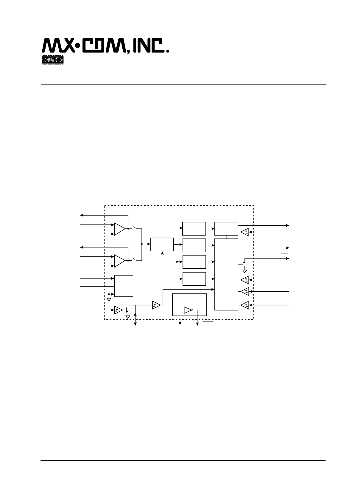
1 Block Diagram
-
+
XTAL
XTAL
-
+
Bandpass
Filters
FSK
Demod
Level
Detector
Detect
Mode
Tone Alert
Detector
Dial T one
Detector
Data
Retiming
Mode
Control
Logic
RXD
To / From µC
RXCLK
IRQ
IN1-
IN2-
IN1+
IN2+
AMPOUT1
Tip & Ring
Hybrid
Rx Output
AMPOUT2
C8
C9
R5
C5
C2
C1
X1
Power
Supply
Circuits
Xtal Osc and
Clock Dividers
DET
RD
RT
V
DD
V
BIAS
V
SS
V
DD
3.579545MHz
MODE 2
MODE 1
INPUT SELECT
Figure 1: Block Diagram
Page 4

Calling Line Identifier with VMWI 4 CMX612 Advance Information
¤1999 MX-COM, Inc. www.mxcom.com tel: 800 638 5577 336 744 5050 fax: 336 744 5054 Doc. # 20480202.002
4800 Bethania Station Road, Winston-Salem, NC 27105-1201 USA All trademarks and service marks are held by their respective companies.
2 Signal List
Package Signal
E3 P6 Name Type
Description
11
XTAL
output The output of the on-chip Xtal oscillator inverter.
2 2 XTAL input The input to the on-chip Xtal oscillator inverter.
3 3 RD input (S) Input to the Ring or Line Polarity Reversal Detector.
4 4 RT bi-directional Open-drain output and Schmitt trigger input forming part of the
Ring or Line Polarity Reversal detector. An external resistor
to V
DD
and a capacitor to VSS should be connected to RT to
filter and extend the RD input signal.
55 INPUT
SELECT
input (S) Controls the selection of the two Input Signal Amplifiers. A
low level selects Input 1 and a high level selects Input 2.
6 6 AMPOUT1 bi-directional The output of on-chip Input Signal Amplifier 1 and an input to
the signal selection multiplexer.
7 7 IN1- input The inverting input to on-chip Input Signal Amplifier 1.
8 8 IN1+ input The non-inverting input to on-chip Input Signal Amplifier 1.
910 V
BIAS
output Internally generated bias voltage, held at VDD/2 when the
device is not in ‘Zero-Power’ mode. Should be bypassed to
V
SS
by a capacitor mounted close to the device pins.
10 11 V
SS
Power Negative supply rail (signal ground).
11 12 IN2+ input The non-inverting input to on-chip Input Signal Amplifier 2.
12 13 IN2- input The inverting input to on-chip Input Signal Amplifier 2.
13 14 AMPOUT2 bi-directional
The output of on-chip Input Signal Amplifier 2 and an input to
the signal selection multiplexer.
14 15 MODE 2 input (S) Input used to select the operating mode. See Section 4.1.
15 16 MODE 1 input (S) As per MODE 2 description.
16 17
IRQ
output An open-drain active low output that may be used as an
Interrupt Request/Wake-up input to the associated PC. An
external pull-up resistor should be connected between this
output and V
DD
.
17 18 DET output
A logic level output driven by the Ring or Line Polarity
Reversal Detector, the Tone Alert Detector, the Dial Tone
Detector or the FSK Level detect circuits, depending on the
operating mode. See Section 4.1.
18 19 RXCLK input (S)
An input that may be used to clock received data bits out of
the FSK Data Retiming block.
19 21 RXD output A logic level output carrying either the raw output of the FSK
Demodulator or re-timed 8-bit characters depending on the
state of the RXCLK input. See Section 4.6
20 22 V
DD
Power The positive supply rail. Levels and thresholds within the
device are proportional to this voltage. Should be bypassed
to V
SS
by a capacitor mounted close to the device pins.
9, 20 Not used. Do not connect to these pins.
Input (S) = Schmitt Trigger Input
Table 1: Signal List
Page 5
Calling Line Identifier with VMWI 5 CMX612 Advance Information
¤1999 MX-COM, Inc. www.mxcom.com tel: 800 638 5577 336 744 5050 fax: 336 744 5054 Doc. # 20480202.002
4800 Bethania Station Road, Winston-Salem, NC 27105-1201 USA All trademarks and service marks are held by their respective companies.
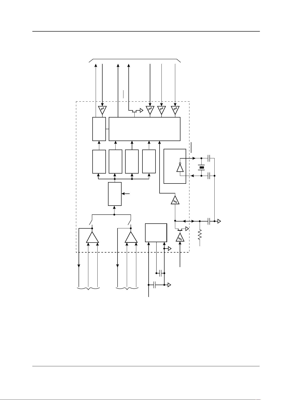
3 External Components
Tip & Ring
20
19
18
17
16
15
10
13
12
11
14
1
2
3
4
5
6
7
8
9
XTAL
XTAL
V
DD
V
SS
V
BIAS
V
BIAS
V
BIAS
IN1+
IN2+
INPUT SELECT
IN1-
IN2-
RD
RT
RXD
RXCLK
DET
IRQ
MODE 1
MODE 2
X1
R1
R2
R3
R4
R5
R8
R6
R7
R9 R10
R13
R12
R11
R17
R16
1:1
2-Wire
Line
R15
R14
R18
D1 - 4
C3
C2
C1
C4
C5
C6
C7
C14
RELAY DRIVER
LOUDSPEAKER
MIC
C13 C12
C11
C8
C9
V
DD
V
DD
V
DD
To/From µC
From µC
Line
Protection
Network
A
B
CMX
612
AMPOUT1
AMPOUT2
Figure 2: Recommended External Components Typical Application
R1
470k
:
C1, C2 18pF
R2 See Section 4.8 C3, C4
0.1PF
R3 – R7
470k
:
C5
0.33PF
R8 Note 1
470k: for V
DD
= 3.3V
680k: for V
DD
= 5.0V
C6, C7 680pF
R9 Note 1
240k: for V
DD
= 3.3V
200k: for V
DD
= 5.0V
C8, C9 Note 2
0.1PF
R10
160k
:
C11, C12 330pF
R11 - R14
100k
:
C13 10nF
R15
600
:
C14 100nF
R16
120k
:
R17
100k
:
X1 Note 3 3.579545MHz
R18
100k: r20%
D1 - D4 1N4004
Resistors r1%, capacitors r20% unless otherwise stated.
Table 2: Recommended External Components for Typical Application
Page 6

Calling Line Identifier with VMWI 6 CMX612 Advance Information
¤1999 MX-COM, Inc. www.mxcom.com tel: 800 638 5577 336 744 5050 fax: 336 744 5054 Doc. # 20480202.002
4800 Bethania Station Road, Winston-Salem, NC 27105-1201 USA All trademarks and service marks are held by their respective companies.
Recommended External Components Notes:
1. Reference Section 4.2
2. It is recommended that the printed circuit board be laid out with a ground plane in the CMX612 area to
provide a low impedance ground connection to the V
SS
pin and to the decoupling capacitors C8 and C9.
3. For best results, a crystal oscillator design should drive the clock inverter input with signal levels of at
least 40% of V
DD
, peak to peak. Tuning fork crystals generally cannot meet this requirement. To obtain
crystal oscillator design assistance, please consult you crystal manufacturer.
4 General Description
4.1 Mode Control Logic
The CMX612's operating mode and the source of the DET and
IRQ
outputs are determined by the logic levels
applied to the MODE 1 and MODE 2 input pins;
MODE 1 MODE 2 Mode DET output from
IRQ
output from
0 0 Tone Alert Detect Tone Alert Signal Detection.
CAS tones present.
Valid ‘off-hook’ CAS or
Ring or Line Polarity
Reversal Detection.
Ringing Signal present.
0 1 FSK Receive FSK Level Detection.
FSK present.
FSK Data Retiming [1] or
Ring or Line Polarity
Reversal Detection.
Ringing Signal present.
1 0 'Zero-Power' Ring or Line Polarity Reversal
Detection.
Ringing Signal present.
Ring or Line Polarity
Reversal Detection.
Ringing Signal present.
1 1 Dial Tone Detect Dial Tone Signal Detection.
Both tones present.
Valid dial tone detected.
[1]
If enabled.
In 'Zero-Power' mode, power is removed from all of the internal circuitry except for the Ring or Line Polarity
Reversal Detector and the DET and
IRQ
outputs.
Page 7
Calling Line Identifier with VMWI 7 CMX612 Advance Information
¤1999 MX-COM, Inc. www.mxcom.com tel: 800 638 5577 336 744 5050 fax: 336 744 5054 Doc. # 20480202.002
4800 Bethania Station Road, Winston-Salem, NC 27105-1201 USA All trademarks and service marks are held by their respective companies.
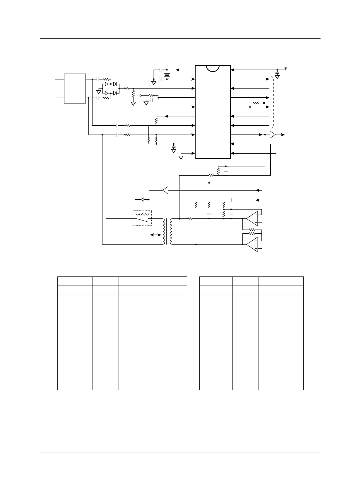
4.2 Input Signal Amplifiers
These amplifiers can be used to convert the balanced FSK, Tone Alert and VMWI signals received over the
telephone line to an unbalanced signal of the correct amplitude for the FSK receiver, Tone Alert and Dial
Tone Detector circuits.
-
+
V
SS
V
BIAS
AMPOUT
IN+
IN-
R8R6
R7
R9 R10
C6
C7
C9
A
B
Input Signal Amplifier
Figure 3: Input Signal Amplifier, balanced input configuration
The design equations for this circuit are;
()
10R-8R
10R
×8R=9R
k160=R10
k470=7R=6R
R9
R8
=
)A-B(V
V
g
ain voltage alDifferenti
AMPOUT
c
c
The target differential voltage gain depends on the expected signal levels between the A and B wires and the
CMX612's internal threshold levels, which are proportional to the supply voltage.
The CMX612 has been designed to meet the applicable specifications with R8 = 430k: at V
DD
= 3.0V
nominal, rising to 680k: at V
DD
= 5.0V, and R9 should be 240k: at V
DD
= 3.0V and 200k: at V
DD
= 5.0V as
shown in Section 3 and Figure 5.
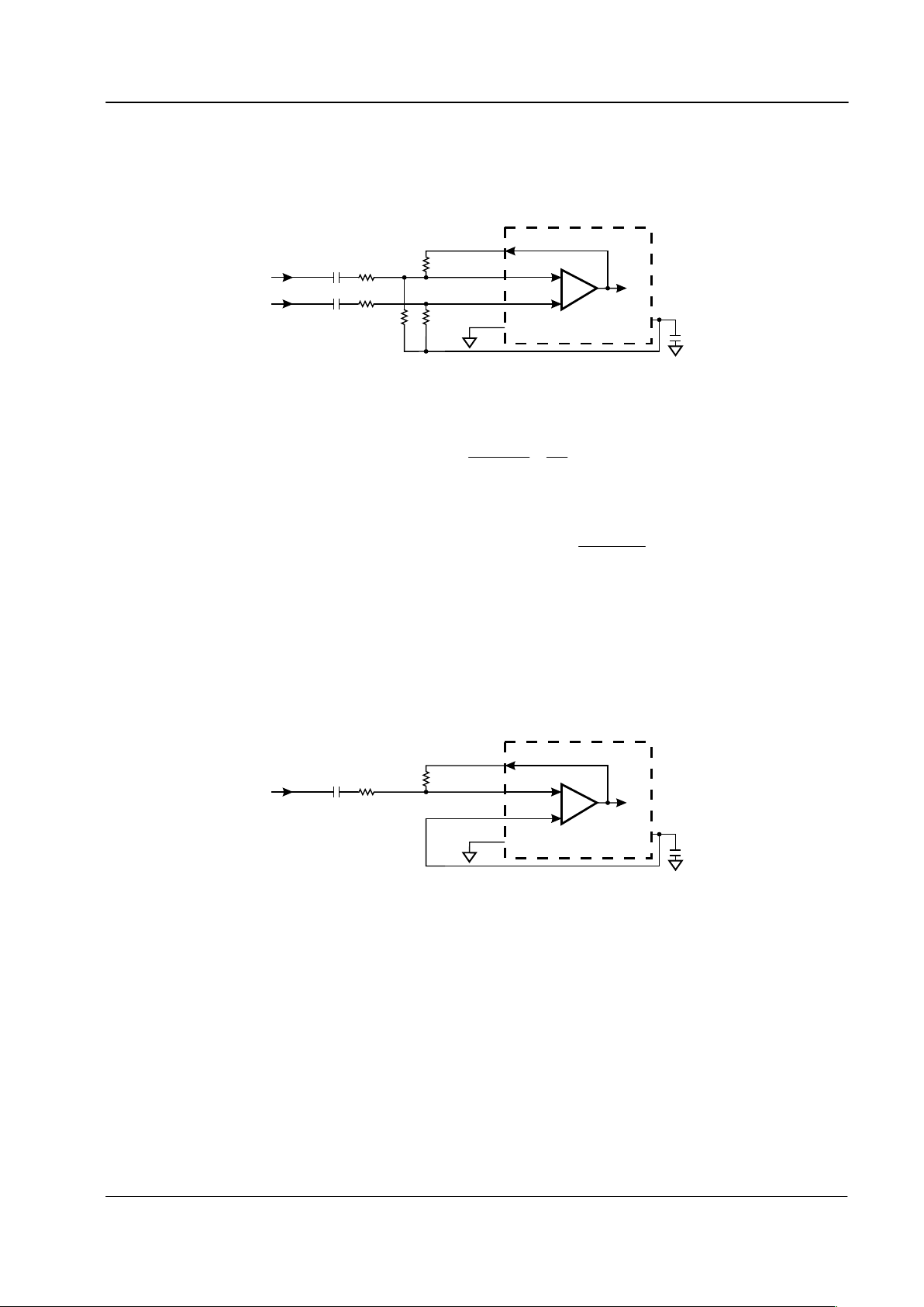
The Input Signal Amplifiers may also be used with an unbalanced signal source as shown in Figure 4. The
values of R6 and R8 are as for the balanced input case.
-
+
V
SS
V
BIAS
AMPOUT
IN+
IN-
R8R6
C6
C9
A
Input Signal Amplifier
Figure 4: Input Signal Amplifier, unbalanced input configuration
Page 8
Calling Line Identifier with VMWI 8 CMX612 Advance Information
¤1999 MX-COM, Inc. www.mxcom.com tel: 800 638 5577 336 744 5050 fax: 336 744 5054 Doc. # 20480202.002
4800 Bethania Station Road, Winston-Salem, NC 27105-1201 USA All trademarks and service marks are held by their respective companies.
0
100
200
300
400
500
600
700
800
900
1000
33.544.55
Nominal V (V)
DD
R8
R9
R8 and R9 : k W
Figure 5: Input Signal Amplifier, optimum values of R8 and R9 vs. V
DD
4.3 Bandpass Filters
These are used to attenuate out of band noise and interfering signals which might otherwise reach the FSK
Demodulator, Tone Alert Detector, Dial Tone detector and Level Detector circuits. The characteristics of
these filters differ in FSK, Tone Alert and Dial Tone modes. Most of the filtering is provided by switched
capacitor stages clocked at 57.7kHz or 9.62kHz depending on mode of operation.
4.4 Level Detector
This block operates by measuring the level of the signal at the output of the Bandpass Filter, and comparing it
against a threshold that depends on whether FSK Receive, Tone Alert Detect or Dial Tone Detect mode has
been selected.
In Tone Alert Detect mode, the output of the Level Detector block provides an input to the Tone Alert Signal
Detector.
In Dial Tone Detect mode, the output of the Level Detector block provides an input to the Dial Tone Signal
Detector.
In FSK Receive mode, the CMX612 DET output will be set high when the level has exceeded the threshold
for sufficient time. Amplitude and time hysteresis are used to reduce chattering of the DET output in marginal
conditions.
Note that in FSK Receive mode this circuit may also respond to non-FSK signals such as speech.
DET
Line Signal
MODE 1
MODE 2
FSK Receiver mode
FSK signal
t
EON
t
EOFF
See Section 6.1 for definitions of t
EON
and t
EOFF
Figure 6: FSK Level Detector Operation
4.5 FSK Demodulator
This FSK Demodulator block converts the 1200 baud FSK input signal to a logic level received data signal
which is output via the RXD pin as long as the Data Retiming function is not enabled (see Section 4.6). This
output does not depend on the state of the FSK Level Detector output.
N
ote:
In the absence of a valid FSK signal, the demodulator may falsely interpret speech or other extraneous
signals as data.
Page 9

Calling Line Identifier with VMWI 9 CMX612 Advance Information
¤1999 MX-COM, Inc. www.mxcom.com tel: 800 638 5577 336 744 5050 fax: 336 744 5054 Doc. # 20480202.002
4800 Bethania Station Road, Winston-Salem, NC 27105-1201 USA All trademarks and service marks are held by their respective companies.
4.6 FSK Data Retiming
The Data Retiming block extracts the 8 data bits of each character from the received asynchronous data
stream, and presents them to the PC under the control of strobe pulses applied to the RXCLK input. The
timing of these pulses is not critical and they may easily be generated by a simple software loop. This facility
removes the need for a UART in the PC without incurring an excessive software overhead.
This block operates on a character by character basis by first looking for the mark to space transition which
signals the beginning of the start bit, then, using this as a timing reference, sampling the output of the FSK
Demodulator in the middle of each of the following 8 received data bits, storing the results in an internal 8-bit
shift register.
When the eighth data bit has been clocked into the internal shift register, the CMX612 examines the RXCLK
input. If this is low then the
IRQ
output will be pulled low and the first of the stored data bits put onto the RXD
output pin. On detecting that the
IRQ
output has gone low, the PC should pulse the RXCLK pin high 8 times.
The high to low transition at the end of the first 7 of these pulses will be used by the CMX612 to shift the next
data bit from the shift register onto the RXD output. At the end of the eighth pulse, the FSK Demodulator
output will be reconnected to the RXD output pin. The
IRQ
output will be cleared the first time the RXCLK
input goes high.
Thus to use the Data Retiming function, the RXCLK input should be kept low until the
IRQ
output goes low; if
the Data Retiming function is not required the RXCLK input should be kept high.
The only restrictions on the timing of the RXCLK waveform are those shown in Figure 7 and the need to
complete the transfer of all eight bits into the PC within 8.3ms (the time of a complete character at 1200
baud).
START STOP
1
1
2
3
4
5
6
7
8
8
Output of FSK Demod :
IRQ output :
RXCLK input :
RXD output :
Received Character 'n'
Retimed data b its fro m
received character 'n'
Data Bit 1 Data Bit 2
t
D
t
D
t
CHI
t
CLO
t
D
IRQ
RXCLK
RXD
tD = Internal CMX612 delay; max. 1Pst
CLO
= RXCLK low time; min 1Pst
CHI
= RXCLK high time; min 1Ps
Figure 7: FSK Operation With Data Retiming
Note:
If enabled, the Data Retiming block will interpret the FSK Channel Seizure signal (a sequence of
alternating mark and space bits) as valid received characters, with values of 55 (hex). Similarly, it may
interpret speech or other signals as random characters.
If the Data Retiming facility is not required, the RXCLK input to the CMX612 should be kept high. The
asynchronous data from the FSK Demodulator will then be connected directly to the RXD output pin, and the
IRQ
output will not be activated by the FSK signal. This case is illustrated in Figure 8.
Page 10

Calling Line Identifier with VMWI 10 CMX612 Advance Information
¤1999 MX-COM, Inc. www.mxcom.com tel: 800 638 5577 336 744 5050 fax: 336 744 5054 Doc. # 20480202.002
4800 Bethania Station Road, Winston-Salem, NC 27105-1201 USA All trademarks and service marks are held by their respective companies.
ST ART
ST ART
STOP
STOP
1
1
2
2
3
3
4
4
5
5
6
6
7
7
8
8
FSK Demod output :
RXD output :
Received Character 'n'
Figure 8: FSK Operation Without Data Retiming (RXCLK always high)
4.7 Tone Alert Detector
This block is enabled when the CMX612 is set to Tone Alert Detect mode. It will then monitor the received
signal for the presence of simultaneous 2130Hz and 2750Hz tones of sufficient level and duration.
Two digital bandpass filters, centered around 2130Hz and 2750Hz, are used within the block to give
additional rejection of interfering signals.
The CMX612 DET output will be set high while a Tone Alert signal is detected.
When the DET output goes low at the end of the Tone Alert signal, then if the DET output had been high for a
time within the CAS qualifying time t
QCAS
limits (see Section 6.1), then the
IRQ
output will be pulled low and
will remain low until the CMX612 is switched out of Tone Alert Detect mode.
Note:
The t
QCAS
timing has been optimized for the detection of 75 to 85ms Tone Alert (CAS) signals used in
off-hook applications, the longer (88 to 110ms) Tone Alert signal employed by British Telecom for on-hook
applications will not necessarily cause
IRQ
to go low.
IRQ
DET
Line Signal
MODE 1
MODE 2
Tone Alert Detect mode
IRQ will only be pulle d low if DET
output was high for t
QCAS
Tone Alert signal
Other mode
t
TON
t
TOFF
See Section 6.1.3 for definitions of t
TON
, t
TOFF
and t
QCAS
Figure 9: Tone Alert Detector Operation
Page 11

Calling Line Identifier with VMWI 11 CMX612 Advance Information
¤1999 MX-COM, Inc. www.mxcom.com tel: 800 638 5577 336 744 5050 fax: 336 744 5054 Doc. # 20480202.002
4800 Bethania Station Road, Winston-Salem, NC 27105-1201 USA All trademarks and service marks are held by their respective companies.
4.8 Dial Tone Detector
This block is enabled when the CMX612 is set to Dial Tone Detect mode. It will then monitor the received
signal for the presence of simultaneous 350Hz and 440Hz tones of sufficient level and duration.
Two digital bandpass filters, centered around 350Hz and 440Hz, are used within the block to give additional
rejection of interfering signals. The CMX612 DET output will be set high while a Dial Tone signal is detected.
When the DET output goes high, the
IRQ
output will be pulled low. It will remain low until the CMX612 is
switched out of Dial Tone Detect mode.
Note:
The Dial Tone Detect timing has been optimized for the detection of >90ms signals. Shorter dial tone
signals will not necessarily be detected.
IRQ
DET
Line Signal
MODE 1
MODE 2
Dial Tone Detect mode
Dial Tone signal
Other mode
t
DON
t
DOFF
See Section 6.1.3 for definitions of t
DON
and t
DOFF
Figure 10: Dial Tone Detector Operation
4.9 Ring or Line Polarity Reversal Detector
These circuits are used to detect the Line Polarity Reversal and Ringing signals associated with the Calling
Line Identification protocol. Figure 11 illustrates their use in a typical application.
Line
IRQ
DET
RD
RT
MODE 1
MODE 2
FromTone Alert,
Energy Detector and
Data Retiming blocks
C5
R1
R2
R5
V
DD
R3
R4
D1 - 4
C3
C4
Line
Protection
Network
A
B
RT
IRQ
(MODE 1 and/or MODE 2 low)
DET
(MODE 1 high and MODE 2 low)
Bridge rectifier output (X)
Ring signal
Vt
HI
V
SS
V
SS
Vt
HI
A
B
X
Figure 11: Ring or Line Polarity Reversal Operation
Page 12

Calling Line Identifier with VMWI 12 CMX612 Advance Information
¤1999 MX-COM, Inc. www.mxcom.com tel: 800 638 5577 336 744 5050 fax: 336 744 5054 Doc. # 20480202.002
4800 Bethania Station Road, Winston-Salem, NC 27105-1201 USA All trademarks and service marks are held by their respective companies.
When no signal is present on the telephone line, RD will be at VSS and RT pulled to VDD by R5 so the output
of the Schmitt trigger 'B' will be low.
The ring signal is usually applied at the subscriber's exchange as an AC voltage inserted in series with one of
the telephone wires and will pass through either C3 and R3 or C4 and R4 to appear at the top end of R1
(point X in Figure 11) in a rectified and attenuated form.
The signal at point X will be further attenuated by the potential divider formed by R1 and R2 before being
applied to the CMX612 input RD. If the amplitude of the signal appearing at RD is greater than the input
threshold (Vt
HI
) of Schmitt trigger 'A' then the N transistor connected to RT will be turned on, pulling the
voltage at RT to V
SS
by discharging the external capacitor C5. The output of the Schmitt trigger 'B' will then
go high, activating the DET and/or
IRQ
outputs depending on the states of the MODE 1 and MODE 2 inputs.
The minimum amplitude ringing signal that is certain to be detected is:
RMSHI
V707.0
2R
3R2R1R
Vt7.0
¸
¹
·
¨
©
§
where Vt
HI
is the high-going threshold voltage of the Schmitt trigger A (see Section 6.1.3).
With R1, R3 and R4 all at 470k:, as Figure 2, setting R2 to 68k: will guarantee detection of ringing signals of
40V
RMS
and above for VDD over the range 2.7 to 5.5V.
A line polarity reversal may be detected using the same circuit but there will be only one pulse at RD. The
British Telecom specification SIN242 says that the circuit must detect a +15V to -15V reversal between the
two lines slewing in 30ms. For a linearly changing voltage at the input to C3 (or C4), then the voltage
appearing at the RD pin will be:
2Re13C
dt
dV
T
t
¸
¸
¹
·
¨
¨
©
§
where T = C3 x (R1 + R2 + R3) and dV/dt is the input slew rate.
For dV/dt = 500V/sec (15V in 30ms), R1, R3 and R4 all 470k: and C3, C4 both 0.1PF as Figure 2, then
setting R2 to 390k: will guarantee detection at V
DD
= 5.5V.
If the time constant of R5 and C5 is large enough then the voltage on RT will remain below the threshold of
the 'B' Schmitt trigger keeping the DET and/or
IRQ
outputs active for the duration of a ring cycle.
The time for the voltage on RT to charge from V
SS
towards VDD can be derived from the formula:
¸
¸
¹
·
¨
¨
©
§
5C5R
t
DDRT
e1VV
As the Schmitt trigger high-going input threshold voltage (Vt
HI
) has a minimum value of 0.56 x VDD, then the
Schmitt trigger B output will remain high for a time of at least 0.821 x R5 x C5 following a pulse at RD.
Using the values given in Figure 2 (470k: and 0.33PF) gives a minimum time of 100 ms (independent of
V
DD
), which is adequate for ring frequencies of 10Hz or above.
If necessary, the PC can distinguish between a ring and a reversal by timing the length of the
IRQ
or DET
output.
4.10 Xtal Osc and Clock Dividers
Frequency and timing accuracy of the CMX612 is determined by a 3.579545MHz clock present at the XTAL
pin. This may be generated by the on-chip oscillator inverter using the external components C1, C2 and X1
of Figure 2, or may be supplied from an external source to the XTAL input, in which case C1, C2 and X1
should not be fitted.
The oscillator is turned off in 'Zero-Power' mode.
If the clock is provided by an external source which is not always running, then the MODE 1 input must be set
high and the MODE 2 input must be set low when the clock is not available. Failure to observe this rule may
cause a significant rise in the supply current drawn by CMX612 as well as generating undefined states of the
RXD, DET and
IRQ
outputs.
Page 13

Calling Line Identifier with VMWI 13 CMX612 Advance Information
¤1999 MX-COM, Inc. www.mxcom.com tel: 800 638 5577 336 744 5050 fax: 336 744 5054 Doc. # 20480202.002
4800 Bethania Station Road, Winston-Salem, NC 27105-1201 USA All trademarks and service marks are held by their respective companies.
5 Application Notes
5.1 'On-Hook' Operation
The systems described in this section operate when the telephone set is not in use (on-hook) to display the
number of a calling party before the call is answered.
5.1.1 Bellcore System
Figure 12 illustrates the line signaling and CMX612 I/O signals for the Bellcore on-hook Caller ID system as
defined in Bellcore documents GR-30-CORE and SR-TSV-002476 and also in ETS 300 659-1 Section 6.1.1
and ETS 300 778-1.
As for the British Telecom system, the 'Chan Seize' signal is a '1010..' FSK bit sequence. The Bellcore
specifications do not require AC or DC line terminations while the FSK data is being received, however
ETS 300 659-1 and ETS 300 778-1 allow for the possibility of an AC termination being applied.
Note:
For simplicity of presentation, the Data Retiming function is not used in Figure 12 (RXCLK is kept
high).
FIRST
RING
CHAN
SEIZE
MARK MESSAGE
RINGING
³ 250ms
3400 to 4400 ms
³ 200ms250ms 150ms
SIGNALING
RD
RT
IRQ
MODE
ZP
DET
RXD
FSK IDLEFSK IDLE FSK DATA
FSK DATA
FSK DATA
Figure 12: Bellcore On-hook System Signals
5.1.2 British Telecom System
Figure 13 illustrates the line signaling and CMX612 I/O signals for the British Telecom on-hook Calling Line ID
system as defined in British Telecom specifications SIN227 and SIN242 part 1. A similar system is described
in ETS 300 659-1 Section 6.1.2c and ETS 300 778-1.
The Tone Alert signal consists of simultaneous 2130Hz and 2750Hz tones, the 'Chan Seize' signal is a
'1010..' FSK bit sequence. Not shown are the requirements for ac and dc loads, including a short initial
Current Wetting Pulse, to be applied to the line 20ms after the end of the Tone Alert signal and to be
maintained during reception of the FSK signal. Note that, for simplicity of presentation, the Data Retiming
function is not used in Figure 13 (RXCLK is kept high).
Page 14

Calling Line Identifier with VMWI 14 CMX612 Advance Information
¤1999 MX-COM, Inc. www.mxcom.com tel: 800 638 5577 336 744 5050 fax: 336 744 5054 Doc. # 20480202.002
4800 Bethania Station Road, Winston-Salem, NC 27105-1201 USA All trademarks and service marks are held by their respective companies.
[1]
IDLE 1 + IDLE 2 5 sec.£
[2]
may go low at end of DET high period, but this is not guaranteed.IRQ
TONE
ALERT
CHAN
SEIZE
MARK MESSAGE
RINGING
Line
reversal
IDLE 1
100ms
4.8 sec
³
<
[1]
[2]
88-110ms > 200ms80-262ms 45-75ms £ 2.5 sec
LINE
SIGNALING
RD
RT
IRQ
MODE
ZP
DET
RXD
IDLE 2
45ms
4.8 sec
³
<
[1]
FSK IDLEFSK IDLE
FSK DATAFSK DATA
Figure 13: British Telecom On-hook System Signals
5.1.3 Other On-hook Systems
ETS 300 659-1 and ETS 300 778-1 also allow for systems where the FSK transmission is preceded by a Dual
Tone Alerting signal similar to that used by British Telecom but without a line reversal (Section 6.1.2a) or by a
Ringing Pulse Alerting Signal (Section 6.1.2b).
The U.K. CCA (Cable Communications Association) specification TW/P&E/312 precedes the FSK signals by
a 200 to 450ms ring burst. The use of ac and dc line terminations during FSK reception is optional.
Mercury Communications Ltd. specification MNR 19 allows for either the British Telecom system or that
specified by CCA.
As these are all slight variants on the British Telecom and Bellcore systems, they can also be handled by the
CMX612.
Page 15

Calling Line Identifier with VMWI 15 CMX612 Advance Information
¤1999 MX-COM, Inc. www.mxcom.com tel: 800 638 5577 336 744 5050 fax: 336 744 5054 Doc. # 20480202.002
4800 Bethania Station Road, Winston-Salem, NC 27105-1201 USA All trademarks and service marks are held by their respective companies.
Yes
Yes
Yes
Yes
Yes
No
No
No
No
No
START:(BT)
CMX612 in ZP mode
START:(Bellcore)
CMX612 in ZP mode
END
Timeout
expired
Line Reversal
Detected ?
End of
ring signal ?
Ring signal
detected ?
CMX612 DET
output high ?
CMX612 DET
output low?
Set CMX612 to
Tone Alert Detect mode.
Start 5 second timeout.
Apply
Current Wetting Pulse,
AC and DC terminations.
Set CMX612 to
FSK Receive mode.
Restart 5 second timeout.
Set CMX612 to
FSK Receive mode.
Start 5 second timeout.
Wait 15ms
Clear timeout.
Remove any AC and DC
line terminations.
Set CMX612 to
Zero Power mode.
Read FSK Message,
display data if
checksum OK.
Figure 14: Flow Chart for On-hook operation of CMX612
Page 16

Calling Line Identifier with VMWI 16 CMX612 Advance Information
¤1999 MX-COM, Inc. www.mxcom.com tel: 800 638 5577 336 744 5050 fax: 336 744 5054 Doc. # 20480202.002
4800 Bethania Station Road, Winston-Salem, NC 27105-1201 USA All trademarks and service marks are held by their respective companies.
5.2 'Off-Hook' Operation
The CIDCW (Calling Identity on Call Waiting) system described in this section operates when the telephone
set is in use (off-hook) to display the number of a waiting caller without interrupting the current call.
Bellcore documents GR-30-CORE and SR-TSV-002476, British Telecom specifications SIN227 and SIN242
Part 2 and ETS 300-659-2 all describe similar systems in which a successful CIDCW transaction consists of a
sequence of actions between the CPE (Customer Premises Equipment - e.g. a telephone) and the Central
Office as indicated in Figure 15.
CAS
ACK
FSK data
D
CE
B
far voice
near voice
Signals originating
from far endCPE
and Central Office
Signals originating
at near end CPE
far voice
near v oice
A
F
A. Normal conversation with both near and far end voice present.
B. Central Office mutes far end voice, sends CAS and becomes silent.
C. CPE recognizes CIDCW initiation and mutes near end voice and keypad.
D. CPE sends DTMF ACK to Central Office to signal its readiness to receive FSK data.
E. Central Office recognizes ACK and sends FSK Caller ID data to CPE.
F. CIDCW transaction is complete. CPE unmutes near end voice and the Central Office unmutes far end
voice, returning to normal conversation.
Figure 15: CIDCW Transaction from Near End CPE Perspective
The CAS signal is transmitted by the Central Office to initiate a CIDCW transaction and consists of an 80ms
burst of simultaneous 2130Hz and 2750Hz tones.
CAS detection is very important because a “missed” signal causes Caller ID information to be lost and a false
signal detection produces a disruptive tone which is heard by the far end caller. Because the CAS signals
must be detected in the presence of conversations which both mask and masquerade as the tone signals, this
function is difficult to accomplish correctly.
Because the numbers of false responses (Talk-offs) and missed signals (Talk-downs) are related to the
speech levels at the CMX612 input, and because the level of near end speech from the local handset is
normally greater than that of far end speech coming from the Central Office, a further improvement in overall
performance can be obtained by taking the CMX612’s audio input from the receive side of the telephone set
hybrid where this is possible.
The internal algorithms used by the CMX612 to drive the DET and
IRQ
outputs in Tone Alert Detect mode
have been optimized for the detection of off-hook CAS signals in the presence of speech when used
according to the following principles:
1. If it is possible to mute the local speech from the microphone rapidly (within 0.5ms) without introducing
noise (i.e. where the CIDCW equipment is built into the telephone set) then this should be done whenever
the CMX612 is in Tone Detect mode and the DET output is high. Doing this will markedly reduce the
number of false responses generated by local (near end) speech. Note that the DET output is not used
for any other purpose in an off-hook application when the CMX612 is set to Tone Alert Detect mode.
2. The
IRQ
output going low when in Tone Alert Detect mode indicates that a CAS has been detected. The
local handset and keypad should then be muted as required by the Bellcore specification and the
CMX612 switched to FSK Receive mode to be ready to receive the FSK data, doing this will also clear
the
IRQ
output.
3. The CMX612’s DET output should be monitored for a period of 50ms after changing to FSK Receive
mode, before sending the ACK signal, and the transaction abandoned if the DET output goes high during
this time, which would be the case if a false CAS detect had been caused by far end speech.
Page 17

Calling Line Identifier with VMWI 17 CMX612 Advance Information
¤1999 MX-COM, Inc. www.mxcom.com tel: 800 638 5577 336 744 5050 fax: 336 744 5054 Doc. # 20480202.002
4800 Bethania Station Road, Winston-Salem, NC 27105-1201 USA All trademarks and service marks are held by their respective companies.
Yes (See Note 2)
Yes
Yes
No
No (See Note 3)
No
START
CMX612 in Tone Alert
Detect mode
2 second timeout
expired
Notes:
1. If it is possible to mute the speech output
from the local microphone quickly and without
introducing noise, then this should be done
whenever the CMX612 DET output is high.
2. The output will be reset by changing
from Tone Alert Detect to FSK Receive mode.
IRQ
3. It may be helpful when monitoring the CMX612
DET output for the 50ms period after changing to
FSK mode to note that changing between Tone
Alert Detect and FSK Receive modes resets the
DET output, which will then remain lo w for at least
15ms, after which if it does go high, it will remain
high for at least 8ms.
IRQ output
low ?
Timer > 50ms ?
CMX612 DET
output high ?
Mute local handset and
keypad.(See Note 1)
Send ACK.
Start 2 second timeout.
Set CMX612 to
FSK Receive mode.
Start timer.
Clear timeout.
Remov e mute from
handset and keypad.
Set CMX612 to
Tone Alert Detect mode.
Read FSK Message,
display data if
checksum OK.
Figure 16: Flow Chart for Off-hook operation of CMX612
Page 18

Calling Line Identifier with VMWI 18 CMX612 Advance Information
¤1999 MX-COM, Inc. www.mxcom.com tel: 800 638 5577 336 744 5050 fax: 336 744 5054 Doc. # 20480202.002
4800 Bethania Station Road, Winston-Salem, NC 27105-1201 USA All trademarks and service marks are held by their respective companies.
5.3 VMWI Operation
VMWI is an indicator for a group of services that is offered by telephone companies to their customers. For
example, it allows voice messages to be stored for later retrieval by the subscribing customer (Voice-Mail
Notification). Messages may be entered into a mailbox by any of the following methods:
1. A call placed to the customer’s line is unanswered after a certain number of rings and is then forwarded to
the voice-mail system (forward on do not answer).
2. A call placed to the customer’s line receives a busy signal and is then forwarded to the voice-mail system
(forward on busy).
3. A message is forwarded to the customer’s voice-mail box by a party directly through the voice-mail
system, without the customer’s line ever being called.
In each case, the presence of messages waiting in the customer’s voice-mail box is indicated to the customer
by generation of a VMWI signal. In Bellcore systems, the identification of a VMWI signal can be performed by
detecting either a Stuttered Dial Tone (off-hook) or an FSK signal (on-hook).
5.3.1 SDT Mode
When there is a message waiting in a customer’s voice-mail box, the telephone company’s Central Office
(CO) switch may apply a special dial tone to the customer’s line when it is taken off-hook. The special dial
tone is called Stuttered Dial Tone and is generally characterized as follows:
1. Steady dial tone frequencies (350Hz + 440Hz).
2. Steady dial tone amplitude up to -12dBV per tone applied from the Central Office (CO) switch to the line.
3. A cadenced signal of 100ms on, 100ms off, repeated between 3 and 10 times and then steady dial tone.
According to the US-FCC Alameda order, the Customer Premises Equipment (CPE) will make a Stuttered
Dial Tone check either:
1. When the subscriber takes the phone off-hook to make a call or
2. within 4 minutes of an unanswered call or
3. within 30 seconds of a completed call.
The telephone is taken off-hook to make a Stuttered Dial Tone check. The CPE then puts the CMX612 from
‘Zero-Power’ mode into Dial Tone Detect mode. If both dial tones are detected, then the DET output will be
set high and the
IRQ
output will be set low.
The DET output may then be polled every 40 - 80ms to check if it has been cleared. The DET output will only
be cleared if one or both tones are removed. If this occurs within 100ms, a counter may be incremented in
the CPE (external to the CMX612) and the
IRQ
output should then be cleared. This may be done by taking
the CMX612 out of Dial Tone Detect mode into ‘Zero-Power’ mode and back into Dial Tone Detect mode.
On receiving another interrupt, the polling routine described above should be repeated. If the counter
reaches an appropriate value (e.g. 10) within an appropriate time (e.g. 2.3 seconds) then Stuttered Dial Tone
has been detected and a visual message indicator will then be lit by the CPE.
Other algorithms to detect Stuttered Dial Tone (e.g. continuous polling of the DET output once an interrupt
has been received) are also possible.
5.3.2 CLASS (FSK) Mode
When there is a message waiting in a customer’s voice-mail box, the telephone company’s Central Office
(CO) switch may send on-hook FSK data to the customer’s line. This can be received by the CMX612 and
used to indicate waiting voice-mail (Voice-Mail Notification) and other CLASS services, by using the FSK
Receive mode.
Page 19

Calling Line Identifier with VMWI 19 CMX612 Advance Information
¤1999 MX-COM, Inc. www.mxcom.com tel: 800 638 5577 336 744 5050 fax: 336 744 5054 Doc. # 20480202.002
4800 Bethania Station Road, Winston-Salem, NC 27105-1201 USA All trademarks and service marks are held by their respective companies.
Yes
Yes
Yes
Yes
Yes
No
No
No
No
No
START
CMX612 in Zero Power
mode.
END
Phone off-hook ?
Unanswered
call or has a ca ll ju s t
completed ?
Both tones detected ?
One or both
tones removed ?
Counter
incremented to
desired value ?
Set CMX612 in Dial Tone
Detect Mode .
DET will be se t h ig h .
will be set low.IRQ
DET will be c le a re d .
Clear .
Increment counter by 1.
IRQ
Stuttered Dial Tone detected.
Visual message
indicator will be lit up.
Figure 17: Flow Chart for VMWI-SDT operation of CMX612
Page 20

Calling Line Identifier with VMWI 20 CMX612 Advance Information
¤1999 MX-COM, Inc. www.mxcom.com tel: 800 638 5577 336 744 5050 fax: 336 744 5054 Doc. # 20480202.002
4800 Bethania Station Road, Winston-Salem, NC 27105-1201 USA All trademarks and service marks are held by their respective companies.
6 Performance Specification
6.1 Electrical Performance
6.1.1 Absolute Maximum Ratings
Exceeding these maximum ratings can result in damage to the device.
Min. Max. Units
Supply (VDD - VSS)-0.37.0V
Voltage on any pin to V
SS
-0.3 V
DD
+ 0.3 V
Current into or out of VDD and V
SS
pins -30 30 mA
Current into or out of any other pin -20 20 mA
E3 Package
Total Allowable Power Dissipation at T
AMB
= 25°C 300 mW
Derating above 25°C5mW/°C above 25°
Storage Temperature -55 125 °C
Operating Temperature -40 85 °C
P6 Package
Total Allowable Power Dissipation at T
AMB
= 25°C 800 mW
Derating above 25°C13mW/°C above 25°
Storage Temperature -55 125 °C
Operating Temperature -40 85 °C
6.1.2 Operating Limits
Correct operation of the device outside these limits is not implied.
Notes Min. Max. Units
Supply (VDD - VSS)2.75.5V
Operating Temperature 2 -40 85 °C
Xtal Frequency 1 3.575965 3.583125 MHz
Notes:
1. An Xtal frequency of 3.579545MHz ±0.1% is required for correct Tone Alert and FSK detection.
2. Operating temperature range -10°C to +60°C at V
DD
< 3.0V.
Page 21

Calling Line Identifier with VMWI 21 CMX612 Advance Information
¤1999 MX-COM, Inc. www.mxcom.com tel: 800 638 5577 336 744 5050 fax: 336 744 5054 Doc. # 20480202.002
4800 Bethania Station Road, Winston-Salem, NC 27105-1201 USA All trademarks and service marks are held by their respective companies.
6.1.3 Operating Characteristics
Details in this section represent design target values and are not currently guaranteed.
For the following conditions unless otherwise specified:
V
DD
= 2.7V at T
AMB
= -10°C to +60°C and V
DD
= 3.0V to 5.5V at T
AMB
= -40°C to +85°C,
Xtal Frequency = 3.579545MHz ± 0.1%, 0dBV corresponds to 1.0V
RMS
.
Notes Min. Typ. Max. Units
DC Parameters
IDD (in ‘Zero-Power’ mode) at V
DD
= 5.0V 1, 2 0.02 TBD µA
IDD (not in ‘Zero-Power’ mode) at V
DD
= 3.0V 1 0.5 TBD mA
IDD (not in ‘Zero-Power’ mode) at V
DD
= 5.0V 1 1.0 TBD mA
Logic ‘1’ input level
(RXCLK and XTAL inputs)
70% V
DD
Logic ‘0’ input level
(RXCLK and XTAL inputs)
30% V
DD
Logic input leakage current (VIN = 0 to VDD)
excluding XTAL input
-1.0 +1.0 µA
Output logic ‘1’ level (lOH = 360µA) VDD -0.4V V
Output logic ‘0’ level (l
OL
= 360µA) 0.4 V
IRQ
output ‘off’ state current (V
OUT
= VDD)
1.0 µA
Schmitt Trigger input thresholds,
see Figure 18
High going (VtHI) 0.56 V
DD
0.56 VDD +0.6V V
Low going (VtLO) 0.44 V
DD
-0.6V 0.44 V
DD
V
Tone Alert Detector
‘Low’ tone nominal frequency 2130 Hz
‘High’ tone nominal frequency 2750 Hz
Start of Tone Alert signal to DET high time
(Figure 9 t
TON
)
55.0 ms
End of Tone Alert signal to DET and
IRQ
low
time (Figure 9 t
TOFF
)
0.5 10.0 ms
DET high time to ensure
IRQ
goes low
(Figure 9 t
QCAS
)
8.0 45.0 ms
To ensure detection:
3
‘Low’ tone frequency tolerance ±0.5 %
‘High’ tone frequency tolerance ±0.5 %
Level (total) 4 -40.0 -2.2 dBV
2750Hz tone level with respect to 2130Hz tone
level
-6.0 +6.0 dB
Signal to Noise ratio 5 20.0 dB
Dual tone burst duration for DET output 75.0 ms
Dual tone burst duration to ensure
IRQ
goes low
75.0 85.0 ms
To ensure non-detection:
6
‘Low’ tone frequency tolerance ±75.0 Hz
‘High’ tone frequency tolerance ±95.0 Hz
Level (total) 4 -46.0 dBV
Dual tone burst duration 45.0 ms
Page 22

Calling Line Identifier with VMWI 22 CMX612 Advance Information
¤1999 MX-COM, Inc. www.mxcom.com tel: 800 638 5577 336 744 5050 fax: 336 744 5054 Doc. # 20480202.002
4800 Bethania Station Road, Winston-Salem, NC 27105-1201 USA All trademarks and service marks are held by their respective companies.
Notes Min. Typ. Max. Units
FSK Receiver
Transmission rate 1188 1200 1212 Baud
V23 Mark (logical 1) frequency 1280 1300 1320 Hz
V23 Space (logical 0) frequency 2068 2100 2132 Hz
Bell202 Mark (logical 1) frequency 1188 1200 1212 Hz
Bell202 Space (logical 0) frequency 2178 2200 2222 Hz
Valid input level range 4 -40.0 -8.0 dBV
Acceptable twist (mark level with respect to
space level)
V23 -6.0 +6.0 dB
Bell202 -10.0 +10.0 dB
Acceptable Signal to Noise ratio
V23 5 20.0 dB
Bell202 5 30.0 dB
Level Detector ‘on’ threshold level 4 -40.0 dBV
Level Detector ‘off’ to ‘on’ time (Figure 6 t
EON
) 25.0 ms
Level Detector ‘on’ to ‘off’ time (Figure 6 t
EOFF
)8.0 ms
Input Signal Amplifier
Input impedance 7 10.0
M
:
Voltage gain 500 V/V
XTAL Input
‘High’ pulse width 8 100 ns
‘Low’ pulse width 8 100 ns
Dial Tone Detector
‘Low’ tone nominal frequency 350 Hz
‘High’ tone nominal frequency 440 Hz
Start of Dial Tone signal to DET high time
(Figure 10 t
DON
)
60.0 ms
End of Dial Tone signal to DET and
IRQ
low
time (Figure 10 t
DOFF
)
3.0 30.0 ms
DET high time (100ms tone duration) 1.3 40.0 60.0 ms
To ensure detection:
3
‘Low’ tone frequency tolerance ±7.0 Hz
‘High’ tone frequency tolerance ±7.0 Hz
Level (per tone) 4 -31.2 -12.2 dBV
350Hz tone level with respect to 440Hz tone
level
-6.0 +6.0 dB
Signal to Noise ratio 5 20.0 dB
Dual tone burst duration for DET output 9 80.0 ms
Dual tone burst duration to ensure
IRQ
goes low
9 80.0 ms
To ensure non-detection:
6
‘Low’ tone frequency tolerance -45.0 +30.0 Hz
‘High’ tone frequency tolerance -30.0 +40.0 Hz
Level (total) 4 -36.0 dBV
Dual tone burst duration 30.0 ms
Page 23

Calling Line Identifier with VMWI 23 CMX612 Advance Information
¤1999 MX-COM, Inc. www.mxcom.com tel: 800 638 5577 336 744 5050 fax: 336 744 5054 Doc. # 20480202.002
4800 Bethania Station Road, Winston-Salem, NC 27105-1201 USA All trademarks and service marks are held by their respective companies.
Notes:
1. At 25
q
C, not including any current drawn from the CMX612 pins by external circuitry other than X1, C1
and C2.
2. RD, RXCLK, MODE 2 inputs at V
SS
, MODE 1 input at VDD. See also Figure 19.
3. All conditions must be met to ensure detection.
4. For V
DD
= 3.3V with equal level tones and with the input signal amplifier external components as
Section 3. The internal threshold levels are proportional to V
DD
. To cater for other supply voltages or
different signal level ranges the voltage gain of the input signal amplifier should be adjusted by selecting
the appropriate external components as described in Section 4.
5. Flat noise in 300 - 3400Hz band for V23, 200 - 3200Hz for Bell202.
6. Meeting any of these conditions will ensure non-detection.
7. Open loop, small signal low frequency measurements.
8. Timing for an external input to the CLOCK/XTAL pin.
9. Tone duration between 80ms and 90ms will normally give 100% detection.
10. Howe ver, under certain conditions (e.g. exact 4:5 ratio between tone frequencies and adverse twist
conditions) up to 0.3% of tones may not be detected. Above 90ms, detection is 100%.
0
0.5
1
1.5
2
2.5
3
3.5
4
3 3.5 4 4.5 5 5.5
V(V)
DD
Vt
HI
Vt
LO
V(V)
IN
Figure 18: Schmitt Trigger typical input voltage thresholds vs. V
DD
0.0001
0.001
0.01
0.1
1
10
-40-30-20-10 0 1020304050607080
Temperature ( C)
o
I(µA)
DD
Figure 19: Typical 'Zero Power' IDD vs. Temperature (VDD = 5.0V)
Page 24

Calling Line Identifier with VMWI 24 CMX612 Advance Information
¤1999 MX-COM, Inc. www.mxcom.com tel: 800 638 5577 336 744 5050 fax: 336 744 5054 Doc. # 20480202.002
4800 Bethania Station Road, Winston-Salem, NC 27105-1201 USA All trademarks and service marks are held by their respective companies.
6.2 Packaging
Figure 20: 20-pin TSSOP (E3) Mechanical Outline:
Order as part no. CMX612E3
NOTE : All dimensions in inches (mm.)
Angles are in degrees
Pac kageTolerances
A
B
C
E
E1
H
TYP. MAX.MIN.DIM.
J
J1
K
L
0.360 (9.14)
0.480 (12.19)
0.128 (3.25)
1.100 (27.94)
0.185 (4.70)
0.420 (10.67)
0.390 (9.91) 0.420 (10.67)
0.020 (0.51)
0.020 (0.51)
0.040 (1.02)
0.066 (1.68)
1.080 (27.43)
0.330 (8.38)
0.100 (2.54)
0.045 (1.14)
0.065 (1.65)
0.015 (0.38)
P
0.010 (0.25)
T
Y
7°
E
Y
E1
T
C
P
J1
K
H
J
L
B
A
PIN 1
Figure 21: 22-pin PDIP (P6) Mechanical Outline:
Order as part no. CMX612P6
 Loading...