

Page 1
DATA BULLETIN
LOW VOLTAGE
CTCSS ENCODER/DECODER
MX465
with Tx and Rx Audio Filters
Features Applications
Meets TIA/EIA-603 Standards
47 CTCSS Tones + Notone
TX/RX Speech Filters
Improved Sinad
Serial or Parallel Programming
Easy µP Interface
Scanning on any Channel
Standard 4MHz Xtal
(See MX165C for 1MHz)
Low Voltage 3.3V to 5.0V
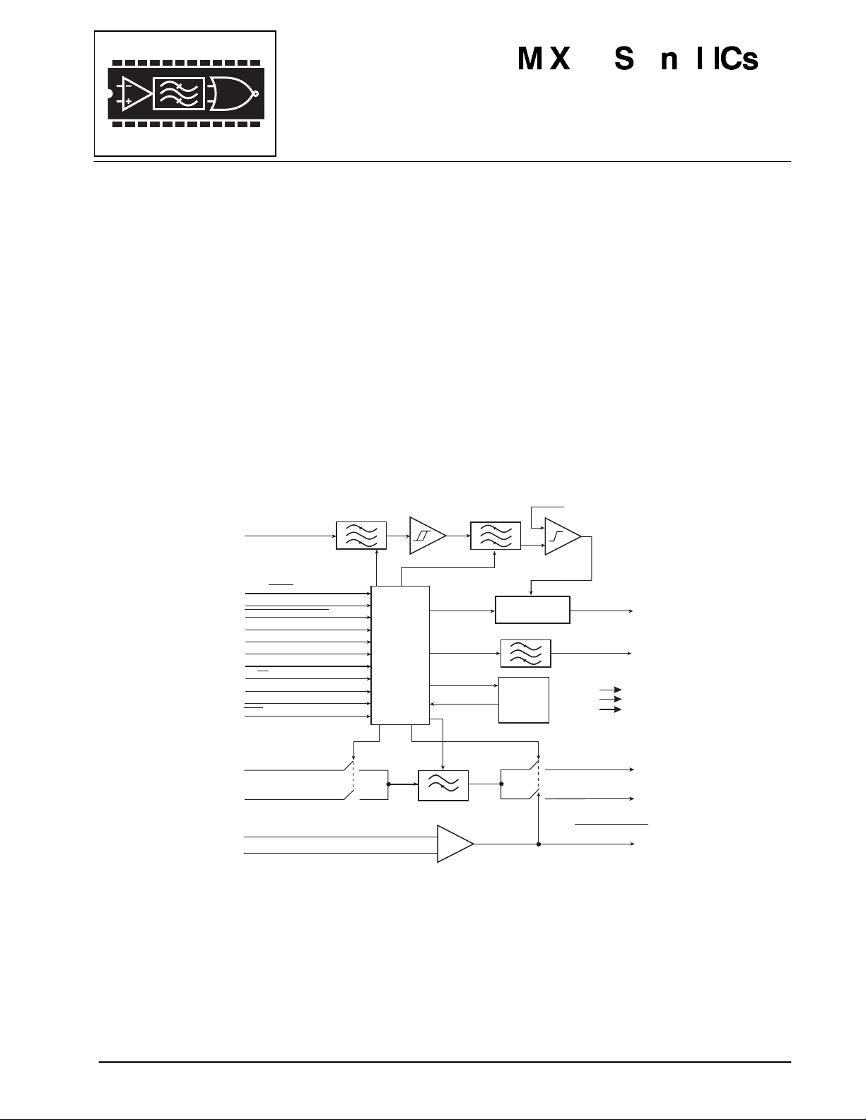
TONE IN
f
LOAD/
LA TCH
D5/SERIAL ENABLE 1
D4/SERIAL ENABLE 2
D3/SERIAL DAT A IN
D2/SERIAL CLOCK
D1
D0
RX/
TX
PTL
XT AL/CLK
XTAL
TONE IN
FILTER
TONE
+
-
CLKS
DIGITAL
INTERFACE
AND
CLOCK
GENERATION
CLKS
CLKS/XTAL
CLKS/XTAL
A0-A5
D0-D10
Mobile Radio Channel Sharing
Scan Trunking
Wireless Intercom Traffic Control
Hookswitch Supervision
Repeater Control
TONE DECODE
FILTER
TONE DETECT
TONE OUT FILTER
LOGIC
TONE
ROM
48 x 10
REFERENCE
VOLTAGE
+
RX TONE DETECT
TX TONE OUT
V
V
V
DD
SS
BIAS
TX AUDIO IN
RX AUDIO IN
DECODE COMPARA T OR REF .
DECODE COMPARA T OR IN
CLK
300Hz
AUDIO FILTER
+
-
TX AUDIO OUT
RX AUDIO OUT
RX TONE DECODE
The MX465 CTCSS Encoder/Decoder is a low voltage, CMOS device that meets TIA/EIA-603 Standards.
The MX465 will encode and decode the tones 159.8Hz, 183.5Hz, 189.9Hz, 196.6Hz, 199.5Hz, 206.5Hz,
229.1Hz, and 254.1Hz in addition to the 39 standard CTCSS tones, for a total of 47 CTCSS tones + Notone.
With the incorporation of the on-chip TX and RX speech filter, the MX465 enhances voice/tone multiplexing by
attenuating TX and RX speech 36dB at frequencies below 250Hz while passing signals > 300Hz with only
1dB of ripple. This not only minimizes CTCSS talk-off in the TX mode but also improves Hum and Noise
performance in the RX mode.
Available in the following package styles: 24-pin TSSOP (MX465TN), 24-pin SSOP (MX465DS),
24-pin SOIC (MX465DW), 24-pin PLCC (MX465LH), 24-pin PDIP (MX465P), and 24-pin CDIP (MX465J) the
MX465 requires a single 3.3V to 5.0V supply and a 4MHz clock or crystal.
©1998 MX•COM, INC. www.mxcom.com Tel: 800 638 5577 336 744 5050 Fax: 336 744 5054 Doc. #20480143.008
4800 Bethania Station Road, winston-Salem, NC 27105-1201 USA All trademarks and service marks are held by their respective companies.
Page 2

Low Voltage CTCSS Encoder/Decoder 2 MX465
CONTENTS
Section Page
1. Block Diagram.................................................................................................................3
2. Signal List........................................................................................................................4
3. External Components..................................................................................................... 6
4. General Description........................................................................................................7
4.1 Description ............................................................................................................................. 7
4.2 I/O Conditions......................................................................................................................... 7
4.3 Filter Response...................................................................................................................... 8
4.4 Serial and Parallel Mode Timing ............................................................................................ 8
4.5 CTCSS Programming...........................................................................................................10
5. Performance Specification........................................................................................... 11
5.1 Electrical Performance......................................................................................................... 11
5.1.1 Absolute Maximum Ratings........................................................................................................11
5.1.2 Operating Limits..........................................................................................................................12
5.2 Packaging............................................................................................................................. 14
MX-COM, Inc. Reserves the right to change specifications at any time and without notice
©1998 MX•COM, INC. www.mxcom.com Tel: 800 638 5577 336 744 5050 Fax: 336 744 5054 Doc. #20480143.008
4800 Bethania Station Road, winston-Salem, NC 27105-1201 USA All trademarks and service marks are held by their respective companies.
Page 3
Low Voltage CTCSS Encoder/Decoder 3 MX465
1 Block Diagram
TONE IN
TONE IN
f
TONE
LOAD/
LATCH
D5/SERIAL ENABLE 1
D4/SERIAL ENABLE 2
D3/SERIAL DATA IN
D2/SERIAL CLOCK
D1
D0
RX/
TX
PTL
XTAL/CLK
XT AL
TX AUDIO IN
RX AUDIO IN
DECODE COMPARATOR REF.
DECODE COMPARATOR IN
FILTER
+
-
CLKS
DIGITAL
INTERFACE
AND
CLOCK
GENERATION
CLKS
CLKS/XTAL
CLKS/XTAL
A0-A5
D0-D10
CLK
300Hz
AUDIO FILTER
+
-
TONE DECODE
FILTER
TONE DETECT
TONE OUT FILTER
48 x 10
LOGIC
TONE
ROM
REFERENCE
VOLT AGE
+
RX TONE DETECT
TX TONE OUT
V
DD
V
SS
V
BIAS
TX AUDIO OUT
RX AUDIO OUT
RX TONE DECODE
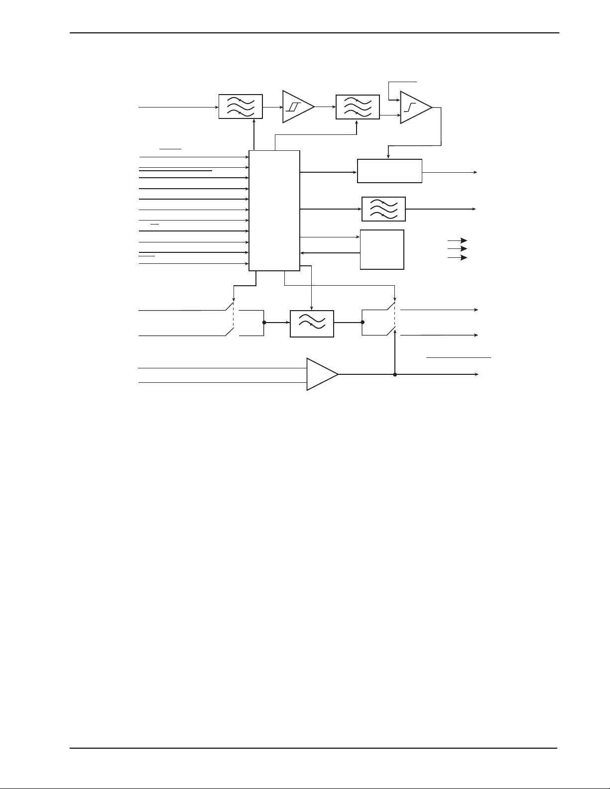
Figure 1 : Block Diagram
©1998 MX•COM, INC. www.mxcom.com Tel: 800 638 5577 336 744 5050 Fax: 336 744 5054 Doc. #20480143.008
4800 Bethania Station Road, winston-Salem, NC 27105-1201 USA All trademarks and service marks are held by their respective companies.
Page 4
Low Voltage CTCSS Encoder/Decoder 4 MX465
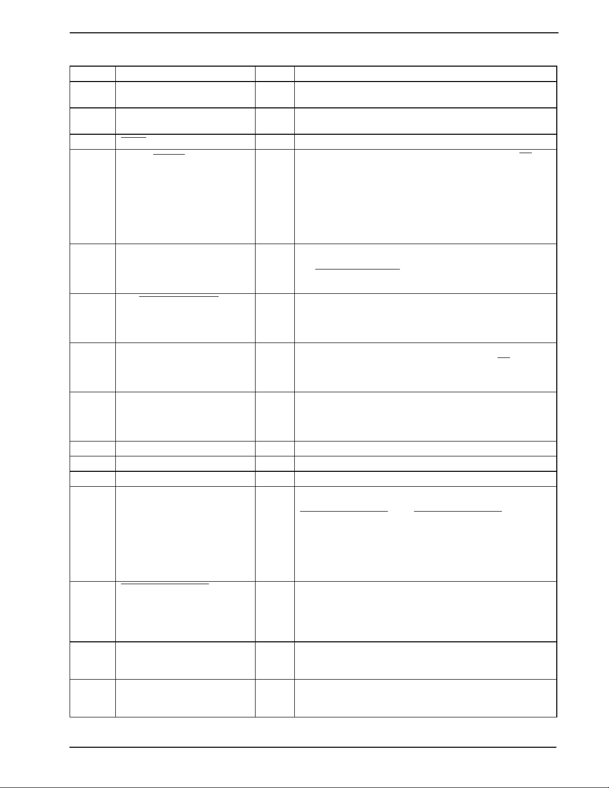
2 Signal List
Pin No. Signal Type Description
1V
DD
2 XTAL/CLOCK input Input to the on-chip inverter used with a 4 MHz Xtal or
3
4
XTAL
LATCH/LOAD
5 D5 / SERIAL ENABLE 1 input Data input D5 (Parallel Mode). A logic 1 applied to this
6
D4 / SERIAL ENABLE 2
7 D3 / SERIAL DATA IN input Data input D3 (Parallel Mode). In Serial Mode this pin
8 D2 / SERIAL CLOCK input Data input D2 (Parallel Mode). In Serial Mode this pin
9 D1 input Data input D1 (Parallel Mode). Internally pulled to VDD.
10 D0 input Data input D0 (Parallel Mode). Internally pulled to VDD.
11 V
SS
12 DECODE COMPARATOR
REF.
13
RX TONE DECODE
14 DECODE COMPARATOR IN input Inverting input of the DECODE COMPARATOR. This pin
15 RX TONE DETECT output In RX mode this output will go to logic 1 during a
power Positive supply. This pin should be bypassed to VSS by
a capacitor mounted close to the device pins.
external clock source.
output Output of the on-chip inverter (clock output).
TX/RX
input Controls 8 on-chip latches. It is used to latch
,
PTL, and D0-D5. A logic 1 applied to this input places the
8 latches in the ‘transparent’ mode. A logic 0 applied to
this input places the 8 latches in the ‘latched’ mode. In
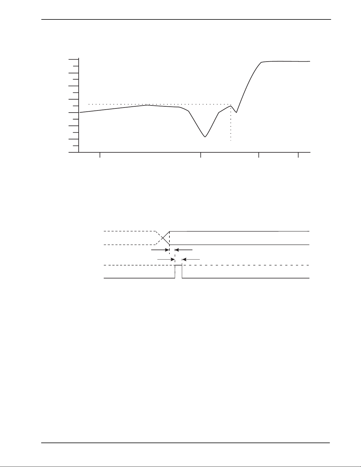
Parallel Mode, data is loaded and latched by a logic 1-0
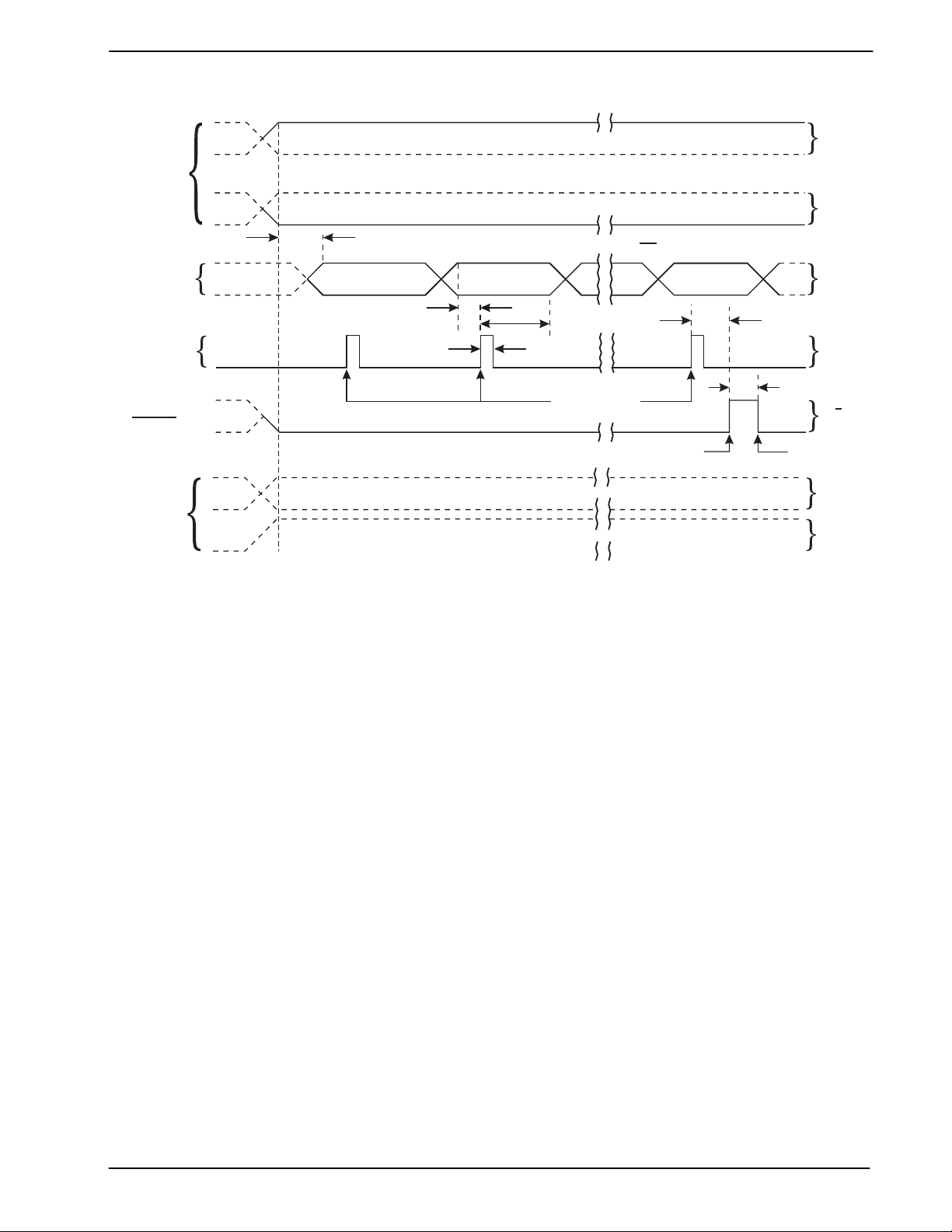
transition (see Figure 4). In Serial Mode, data is loaded
and latched by a 0-1-0 strobe pulse on this pin (see
Figure 5). Internally pulled to V
DD
input together with a logic 0 applied to
D4/SERIAL ENABLE 2
Mode (see Figure 5). Internally pulled to V
will place the device in Serial
.
DD
input Data input D4 (Parallel Mode). A logic 0 applied to this
input together with a logic 1 applied to D5 / SERIAL
ENABLE 1 will place the device in Serial Mode
(see Figure 5). Internally pulled to V
becomes the serial data input for D5-D0,
DD
.
TXRX/
and PTL
(see Figure 5). D5 is clocked first and PTL last.
Internally pulled to V
DD
.
becomes the SERIAL CLOCK input. Data is clocked on
the positive going edge (see Figure 5). Internally pulled
to V
.
DD
power Negative supply.
input Internally biased to VDD/3 or 2 VDD/3 via 1M resistors
depending on the logic state of the
RX TONE DECODE
bias this input 2 V
DD
RX TONE DECODE
pin.
= 1 will
/3; a logic 0 will bias this input VDD/3.
This input provides the DECODE COMPARATOR
REFERENCE voltage, and the switching of bias voltages
provides hysteresis to reduce ‘chatter’ under marginal
conditions.
output Gated output of the decode comparator. This output is
used to gate the RX Audio path. A logic 0 on this pin
indicates a successful decode and the DECODE
COMPARATOR IN pin is more positive than the
DECODE COMPARATOR REF. input (see Table 3).
is normally connected to the integrated output of the RX
TONE DETECT line.
successful decode. It must be externally integrated to
control response and deresponse times (see Table 3).
©1998 MX•COM, INC. www.mxcom.com Tel: 800 638 5577 336 744 5050 Fax: 336 744 5054 Doc. #20480143.008
4800 Bethania Station Road, winston-Salem, NC 27105-1201 USA All trademarks and service marks are held by their respective companies.
Page 5
Low Voltage CTCSS Encoder/Decoder 5 MX465
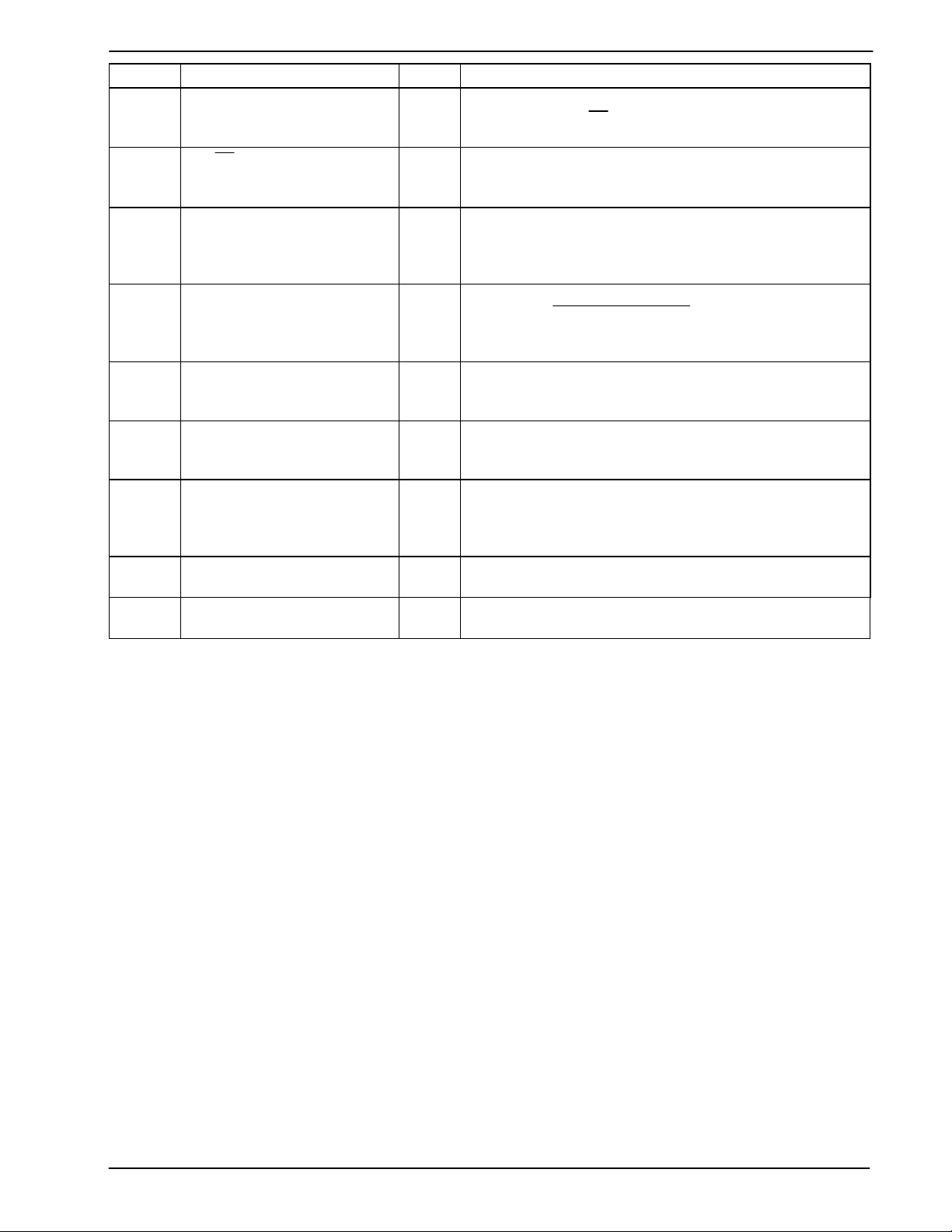
Pin No. Signal Type Description
16 TX TONE OUT output The CTCSS sinewave output appears on this pin under
17
control of the
TX TONE OUT may be biased to V
TXRX/
input RX or TX modes selected in Parallel Mode (see Figure
pin. When not transmitting a tone,
TXRX/
/2. (see Table 3).
DD
4). In Serial Mode this function is serially loaded. This
pin is internally pulled to V
via a 1M resistor.
DD
18 PTL input In RX mode this pin operates as a ‘Push To Listen’
function by enabling the RX audio path, thus overriding
the tone squelch function (Parallel Mode). In Serial Mode
this function is loaded serially. Internal pull-up to V
DD
19 RX AUDIO OUT output High pass filtered RX AUDIO OUT. This pin outputs
audio when
RX TONE DECODE
= logic 0, PTL = logic 1,
or when Notone is programmed (see Table 4). In TX
mode this pin is biased to V
DD
/2.
20 TX AUDIO OUT output High pass filtered TX AUDIO OUT pin. In TX mode this
pin outputs audio present at the TX AUDIO IN pin. In RX
21 V
BIAS
mode this pin is biased to V
output Output of an internally generated VDD /2 bias level that
would normally be externally bypassed to V
DD
/2
SS
via
capacitor C6.
22 TX AUDIO IN input In TX mode TX AUDIO IN may be prefiltered, using the
TX Audio path, thus helping to avoid talk-off due to
intermodulation of speech frequencies with the
transmitted CTCSS tone. Internally biased to V
DD
/2.
23 RX AUDIO IN input Input to the audio high pass filter in RX mode. Internally
biased to V
DD
/2.
24 TONE INPUT input Input to the CTCSS tone detector. Internally biased to
V
/2.
DD
Table 1: Signal List
©1998 MX•COM, INC. www.mxcom.com Tel: 800 638 5577 336 744 5050 Fax: 336 744 5054 Doc. #20480143.008
4800 Bethania Station Road, winston-Salem, NC 27105-1201 USA All trademarks and service marks are held by their respective companies.
Page 6
Low Voltage CTCSS Encoder/Decoder 6 MX465
3 External Components
V
DD
C1
C2
C3
DECODE COMPARATOR REF.
R1X1
LOAD / LATCH
D5/SERIAL ENABLE 1
D4/SERIAL ENABLE 2
D3/SERIAL DATA IN
D2/SERIAL CLOCK
V
DD
XTAL/CLK
XTAL
D1
D0
V
1
2
3
4
5
6
MX465
7
8
9
10
SS
11
12
TONE IN
24
RX AUDIO IN
23
TX AUDIO IN
22
V
21
20
19
18
17
16
15
14
13
BIAS
TX AUDIO OUT
RX AUDIO OUT
PTL
RX / TX
TONE OUT
RX TONE DETECT
DECODE COMPARATOR IN
RX TONE DECODE
C4
C5
C10
C6
C11
C7
C8
R3
R2
D1
C9
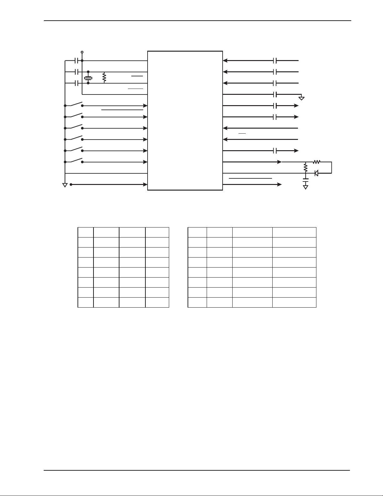
Figure 2 : Recommended External Components for Typical Application
R1 Note 1
R2
R3
C1
1.0M
560k
820k
0.1F20%
C2 Note 1 18pF
C3 Note 1 33pF
C4 Note 2
C5 Note 2
0.1F20%
0.1F20%
10%
10%
10%
20%
20%
C6
C7 Note 2
C8 Note 2
C9 Note 2
C10 Note 2
C11 Note 2
0.47F
0.1F
0.1F
0.1F
0.1F
0.1F
20%
20%
20%
20%
20%
20%
D1 small signal
X1 Note 1 4MHz 100ppm max.
Table 2: External Components
External Components Notes:
1. The values specified for R1, C2, and C3 have been found to be satisfactory when used with a crystal
(X1) whose equivalent series resistance is 1000. For best results, a crystal oscillator design should
drive the clock inverter input with signal levels of at least 40% of V
, peak to peak. Tuning fork
DD
crystals generally cannot meet this requirement. To obtain crystal oscillator design assistance, consult
your crystal manufacturer.
2. The 0.1F value for the DC Blocking capacitors, C4, C5, C7, C8, C9, C10, and C11 is not a
requirement. For the capacitors C4, C5, and C10, the input impedance is internal to the device and
specified typical as 550k. For the remaining capacitors external circuits will be important in
determining the input impedance.
©1998 MX•COM, INC. www.mxcom.com Tel: 800 638 5577 336 744 5050 Fax: 336 744 5054 Doc. #20480143.008
4800 Bethania Station Road, winston-Salem, NC 27105-1201 USA All trademarks and service marks are held by their respective companies.
Page 7
Low Voltage CTCSS Encoder/Decoder 7 MX465
4 General Description
4.1 Description
Voice on shared radio channels are multiplexed with a subaudible CTCSS (Continuous Tone Controlled
Subaudible Squelch) tone as a means of directing messages among user groups sharing the same RF
frequencies. CTCSS modulates the transmitter with a discrete tone, from 39 standard CTCSS tones in the
range (67.0Hz to 250.0Hz) according to TIA/EIA-603. There are an additional eight CTCSS tones not
specified in TIA/EIA-603 that the MX465 will encode and decode. They are : 159.8Hz, 183.5Hz, 189.9Hz,
196.6Hz, 199.5Hz, 206.5Hz, 229.1Hz, and 254.1Hz, for a total of 47 CTCSS tones plus Notone.
The MX465 also incorporates TX/RX on chip speech filters. In early CTCSS designs, TX speech was not
filtered from the CTCSS tone, rather the filtering was dependent upon the host transmitter’s pre-emphasis
network. At only 6dB/octave, the attenuation of speech components at higher CTCSS tones was only a few
dB which resulted in talk-off (low frequency voice components unsquelching the receiver audio).
4.2 I/O Conditions
D0-D5
Tone No Tone Tone Tone Tone No Tone
Input Pins Condition
RX TX/
001111
PTL 0 X 0 1 X X
Decode Comparator In X X 0 0 1 X
Output Pins Condition
RX TONE DETECT 00001X
RX TONE DECODE
111100
Result / Function
Tone Transmitter Enabled Yes No (Bias) No (Bias) No (Bias) No (Bias) No (Bias)
TX Audio Path Enabled Yes Yes No No No No
Tone Decode Enabled No No Yes Yes Yes Yes
RX Audio Path Enabled No (Bias) No (Bias) No (Bias) Yes Yes Yes
Notes 123456
Notes:
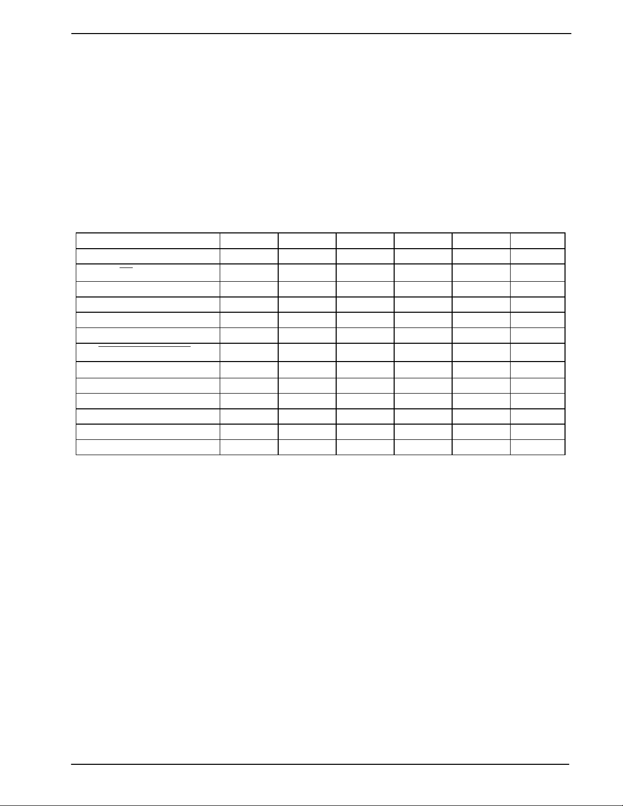
1. Normal tone transmit condition.
2. Notone programmed in TX mode, tone transmit output set to V
/2. TX audio path enabled.
DD
3. Normal decode standby.
4. Normal decode standby with PTL used to enable audio.
5. Normal decode of correct CTCSS tone condition, PTL has no effect.
6. Notone programmed in RX mode, tone transmit output (Bias). RX audio path enabled.
7. X =don’t care
Table 3: Combinations of Input / Output conditions
©1998 MX•COM, INC. www.mxcom.com Tel: 800 638 5577 336 744 5050 Fax: 336 744 5054 Doc. #20480143.008
4800 Bethania Station Road, winston-Salem, NC 27105-1201 USA All trademarks and service marks are held by their respective companies.
Page 8
Low Voltage CTCSS Encoder/Decoder 8 MX465
4.3 Filter Response
Gain (dB)
0
-10
-20
CTCSS Frequencies
-30
-33
-40
-50
-60
-70
100
Figure 3 : Voiceband Filter Response
4.4 Serial and Parallel Mode Timing
D0-D5
RX/TX, PTL
LOAD/LATCH
200
Frequency (Hz)
t
SP
t
L
250.3
V oiceband Frequencies
300
400
Figure 4 : Parallel Mode
©1998 MX•COM, INC. www.mxcom.com Tel: 800 638 5577 336 744 5050 Fax: 336 744 5054 Doc. #20480143.008
4800 Bethania Station Road, winston-Salem, NC 27105-1201 USA All trademarks and service marks are held by their respective companies.
Page 9
Low Voltage CTCSS Encoder/Decoder 9 MX465
1
D5
0
SERIAL
ENABLE
1
D4
DA T A
(Note)
SERIAL
CLOCK
LOAD/
LATCH
0
1
0
0
t
1
DA TA D5 DA TA D4
D3
RX/TX
PTL
D3
t
SS
t
t
C
H
t
2
D2
t
L
LOAD DATA
L/L
LATCH DATA
DA T A
LATCHED
DON'T
DON'T CARE - 1M PULL UPΩ
CARE
DON'T CARE - 1M PULL UPΩ
Note : Serial bit 1 through bit 8 = D5, D4, D3, D2, D1, D0, RX/TX and PTL respectively. Load bit 1 first, bit 8 last
Figure 5 : Serial Mode
D1
D0
©1998 MX•COM, INC. www.mxcom.com Tel: 800 638 5577 336 744 5050 Fax: 336 744 5054 Doc. #20480143.008
4800 Bethania Station Road, winston-Salem, NC 27105-1201 USA All trademarks and service marks are held by their respective companies.
Page 10
Low Voltage CTCSS Encoder/Decoder 10 MX465
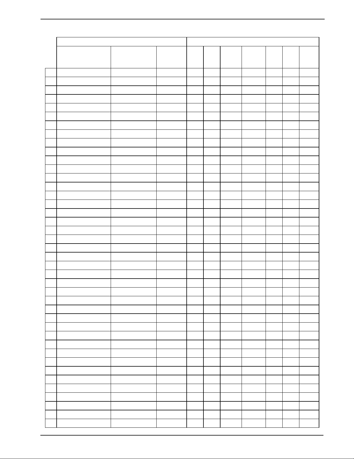
4.5 CTCSS Programming
Tone Programming Inputs
Nominal
Frequency (Hz)
67.0 66.98 -0.029 1 1 1 1 1 1 3F
69.3 69.32 0.024 1 1 1 0 0 1 39
71.9 71.901 0.001 0 1 1 1 1 1 1F
74.4 74.431 0.042 1 1 1 1 1 0 3E
77.0 76.965 -0.046 0 0 1 1 1 1 0F
79.7 79.677 -0.029 1 1 1 1 0 1 3D
82.5 82.483 -0.021 0 1 1 1 1 0 1E
85.4 85.383 -0.020 1 1 1 1 0 0 3C
88.5 88.494 -0.007 0 0 1 1 1 0 0E
91.5 91.456 -0.048 1 1 1 0 1 1 3B
94.8 94.76 -0.042 0 1 1 1 0 1 1D
97.4 97.435 -0.036 1 1 1 0 1 0 3A
100.0 99.96 -0.040 0 0 1 1 0 1 0D
103.5 103.429 -0.069 0 1 1 1 0 0 1C
107.2 107.147 -0.05 0 0 1 1 0 0 0C
110.9 110.954 0.049 0 1 1 0 1 1 1B
114.8 114.84 0.035 0 0 1 0 1 1 0B
118.8 118.793 -0.006 0 1 1 0 1 0 1A
123.0 123.028 0.023 0 0 1 0 1 0 0A
127.3 127.328 0.022 0 1 1 0 0 1 19
131.8 131.674 -0.095 0 0 1 0 0 1 09
136.5 136.612 0.082 0 1 1 0 0 0 18
141.3 141.323 0.016 0 0 1 0 0 0 08
146.2 146.044 -0.107 0 1 0 1 1 1 17
151.4 151.441 0.027 0 0 0 1 1 1 07
156.7 156.875 0.112 0 1 0 1 1 0 16
• 159.8 159.936 0.085 1 1 0 0 0 1 31
162.2 162.311 0.069 0 0 0 1 1 0 06
167.9 167.708 -0.114 0 1 0 1 0 1 15
173.8 173.936 0.078 0 0 0 1 0 1 05
179.9 179.654 -0.137 0 1 0 1 0 0 14
• 183.5 183.680 0.098 1 1 0 0 1 0 32
186.2 186.289 0.048 0 0 0 1 0 0 04
• 189.9 190.069 0.089 1 1 0 0 1 1 33
192.8 192.864 0.033 0 1 0 0 1 1 13
• 196.6 196.329 -0.138 1 1 0 1 0 0 34
• 199.5 199.312 -0.094 1 1 0 1 0 1 35
203.5 203.645 0.071 0 0 0 0 1 1 03
• 206.5 206.207 -0.142 1 1 0 1 1 0 36
210.7 210.848 0.070 0 1 0 0 1 0 12
218.1 217.853 -0.113 0 0 0 0 1 0 02
MX465
Frequency
(Hz)
f0 (%)
D5 D4 D3 D2 D1 D0 Hex
©1998 MX•COM, INC. www.mxcom.com Tel: 800 638 5577 336 744 5050 Fax: 336 744 5054 Doc. #20480143.008
4800 Bethania Station Road, winston-Salem, NC 27105-1201 USA All trademarks and service marks are held by their respective companies.
Page 11
Low Voltage CTCSS Encoder/Decoder 11 MX465
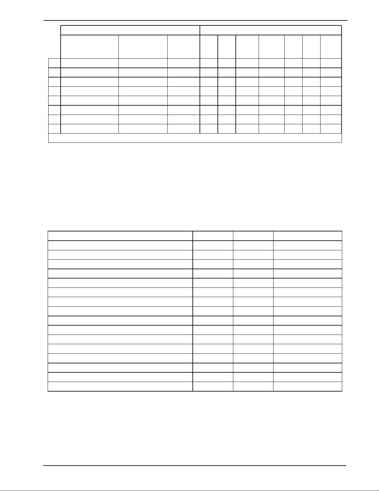
Tone Programming Inputs
Nominal
Frequency (Hz)
MX465
Frequency
f0 (%)
D5 D4 D3 D2 D1 D0 Hex
(Hz)
225.7 225.339 -0.160 0 1 0 0 0 1 11
• 229.1 229.279 0.078 1 1 0 1 1 1 37
233.6 233.359 -0.103 0 0 0 0 0 1 01
241.8 241.970 0.070 0 1 0 0 0 0 10
250.3 250.282 -0.007 0 0 0 0 0 0 00
• 254.1 254.162 0.024 1 1 1 0 0 0 38
Notone N/A 1 1 0 0 0 0 30
Serial input mode N/A 1 0 Data Clock X X 2X
• Not specified in the TIA/EIA tone set
Table 4: CTCSS Tones
5 Performance Specification
5.1 Electrical Performance
5.1.1 Absolute Maximum Ratings
Exceeding these maximum ratings can result in damage to the device. Operation of the device outside the
operating limits is not implied.
General Min. Max. Units
Supply (VDD - VSS) -0.3 7.0 V
Voltage on any pin to V
SS
-0.3 V
+ 0.3 V
DD
Current
V
DD
V
SS
-30 30 mA
-30 30 mA
any other pins -20 20 mA
TN / DW / LH / DIP Package
Total Allowable Power Dissipation at T
=25°C 800 mW
AMB
Derating above 25°C 10 mW/°C above 25°C
Storage Temperature -55 125 °C
Operating temperature - 40 85 °C
DS Package
Total Allowable Power Dissipation at T
=25°C 550 mW
AMB
Derating above 25°C 9 mW/°C above 25°C
Storage Temperature -55 125 °C
Operating temperature - 40 85 °C
©1998 MX•COM, INC. www.mxcom.com Tel: 800 638 5577 336 744 5050 Fax: 336 744 5054 Doc. #20480143.008
4800 Bethania Station Road, winston-Salem, NC 27105-1201 USA All trademarks and service marks are held by their respective companies.
Page 12
Low Voltage CTCSS Encoder/Decoder 12 MX465
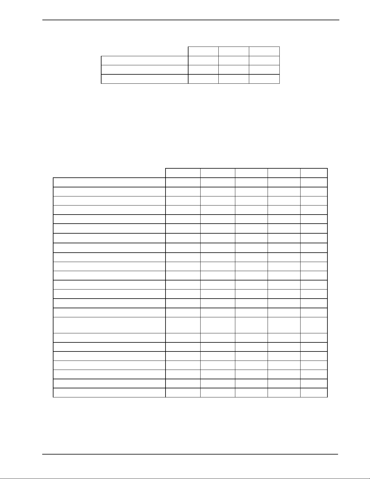
5.1.2 Operating Limits
Correct operation of the device outside these limits is not implied.
Min. Max. Units
Supply (VDD-VSS)2.75.5V
Xtal Frequency 4.0 4.0 MHz
Operating Temperature -40 85 °C
5.1.3 Operating Characteristics
For the following conditions unless otherwise specified:
= 3.3V / 5.0V at T
V
DD
AMB
= 25°C, V
SS
= 0V,
Xtal Frequency = 4.0 MHz, 100ppm max.
(Over the life of the XTAL the operating range may vary from 100ppm up to 1000ppm)
0dB ref. = 750mV
Composite Signal
1kHz test tone = 300mV
(proportional to VDD; see note 17)
RMS
:
, f0 CTCSS tone = 30 mV
RMS
RMS
, 75mV
Noise (band limited to 6kHz
RMS
Gaussian)
Notes Min. Typ. Max. Units
Static Values
Supply voltage 2.7 3.3/5.0 5.5 V
Supply current
VDD = 5.0V 3.7 4.2 mA
VDD = 3.3V 1.3 1.6 mA
Analog input impedance 18 480 550
Analog output impedance 18 400 1000
Digital Input impedance 1,18 25 40
Input logic 1 1 70%V
DD
Input logic 0 1 30%V
Output Logic 1 source = 0.1mA 2 80%V
DD
Output Logic 0 sink = 0.1mA 2 20%V
DD
DD
k
k
V
V
V
V
Dynamic Values
Speech filter
Total harmonic distortion 5,8,19 1.0 1.5 %
Output noise level (input AC short
8,18 0.5 1.0 mV
RMS
circuit, audio switch enabled)
Sinad 8,9 40 50 dB
Spurious emissions 18 - 48 dB
Cutoff frequency 300 Hz
Bandpass ripple 8 1 1.8 dB
Stopband attenuation <250Hz 7,8,19 33 36 dB
Passband gain 1kHz - 0.5 0 0.5 dB
TX/RX isolation 5 60 dB
©1998 MX•COM, INC. www.mxcom.com Tel: 800 638 5577 336 744 5050 Fax: 336 744 5054 Doc. #20480143.008
4800 Bethania Station Road, winston-Salem, NC 27105-1201 USA All trademarks and service marks are held by their respective companies.
Page 13
Low Voltage CTCSS Encoder/Decoder 13 MX465
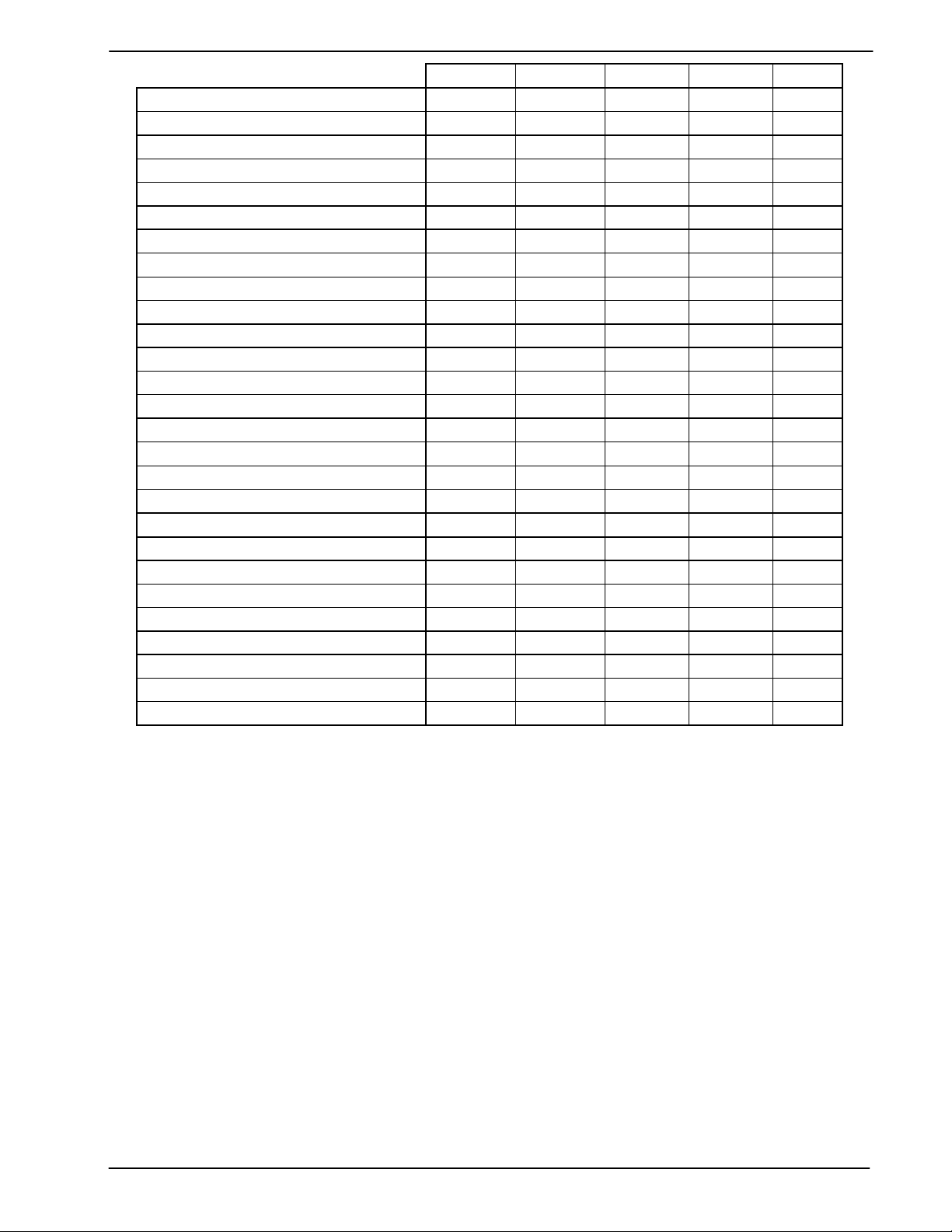
Notes Min. Typ. Max. Units
Encoder
Tone output level 12 - 1.0 0 1.0 dB
Tone Frequency Accuracy (f error) - 0.3 0.3 %f
0
Risetime to 90% nominal output
f0>100Hz 4,10 15 75 ms
f0<100Hz 4,10 45 120 ms
Total Harmonic Distortion 19 1.5 2 %
Decoder
Pure tone decode threshold 19 7 15 mV
Composite signal decode threshold 3 30 mV
RMS
RMS
Decode input signal level 16 -20 3.5 dB
Pure tone decode response time 13,14 95 115 140 ms
Pure tone decode deresponse time 13,15 95 130 170 ms
Decode response time 3,6,10 250 ms
Deresponse time 3,10 180 250 ms
Decode selectivity:
Upper decode band edge 3,11,19,20 1.005f
Lower decode band edge 3,11,19,20 1.005f
0-1
1.015f
0
0.985f
0.995f
0
0
0.995f
0+1
0
Hz
Hz
Serial / Parallel Inputs
Parallel Set Up Time (tSP) 400 ns
Load / Latch Pulse Width (tL) 400 ns
Serial Clock Pulse Width (tC) 400 ns
Serial Data Set-Up Time (tSS) 400 ns
Serial Data Hold Time (tH) 400 ns
Serial Enable Time (t1) 400 ns
Serial Load / Latch Set-Up Time (t2) 400 ns
Serial Clock Frequency 1 MHz
Operating Characteristics Notes:
1. Refers to RX/TX, PTL, Decode Comparator Input, D0-D5.
2. All logic outputs.
3. Composite signal test condition.
4. Any programming tone and R
= 10k, CL = 15pF.
L
5. With an input level of 0dB @1kHz
6. f
>100Hz (for 100 Hz> f0>67Hz: t=100/ f0Hz x 250ms)
0
7. See Figure 3.
8. Measured in a 30kHz bandwidth.
9. With an input level of -3.5dB @1kHz
10. Per TIA/EIA-603.
11. Per TIA/EIA-603, device will not decode adjacent TIA/EIA-603 Tones.
12. Tone output level is proportional to V
=156.7Hz @ -20dB.
13. f
0
DD
.
14. Typically 12.5 Tone Cycles + 40ms.
15. Typically 7 Tone Cycles + 90ms.
©1998 MX•COM, INC. www.mxcom.com Tel: 800 638 5577 336 744 5050 Fax: 336 744 5054 Doc. #20480143.008
4800 Bethania Station Road, winston-Salem, NC 27105-1201 USA All trademarks and service marks are held by their respective companies.
Page 14
Low Voltage CTCSS Encoder/Decoder 14 MX465
16. Max composite signal is 3.5dB with:
Noise (band limited 6kHz Gaussian) = -12dB ref to 1kHz test tone
CTCSS tone = -20dB ref to 1kHz test tone
f
0
17. For maximum dynamic range, set audio level to 0dB, V
x150mV
DD
which system is intended to work. (e.g. for a 2.7V system, use 0dB equal to 405mV
, using minimum VDD under
RMS
RMS
).
18. By characterization only.
19. Batch sampled only
20. For example, if: f
= 100.0Hz (f
0
= 97.4Hz f
0-1
= 103.5Hz)
0+1
Decode Selectivity Min Typ Max Unit
Upper Decode Band Edge 100.5 101.5 102.98 Hz
Lower Decode Band Edge 97.89 98.5 99.5 Hz
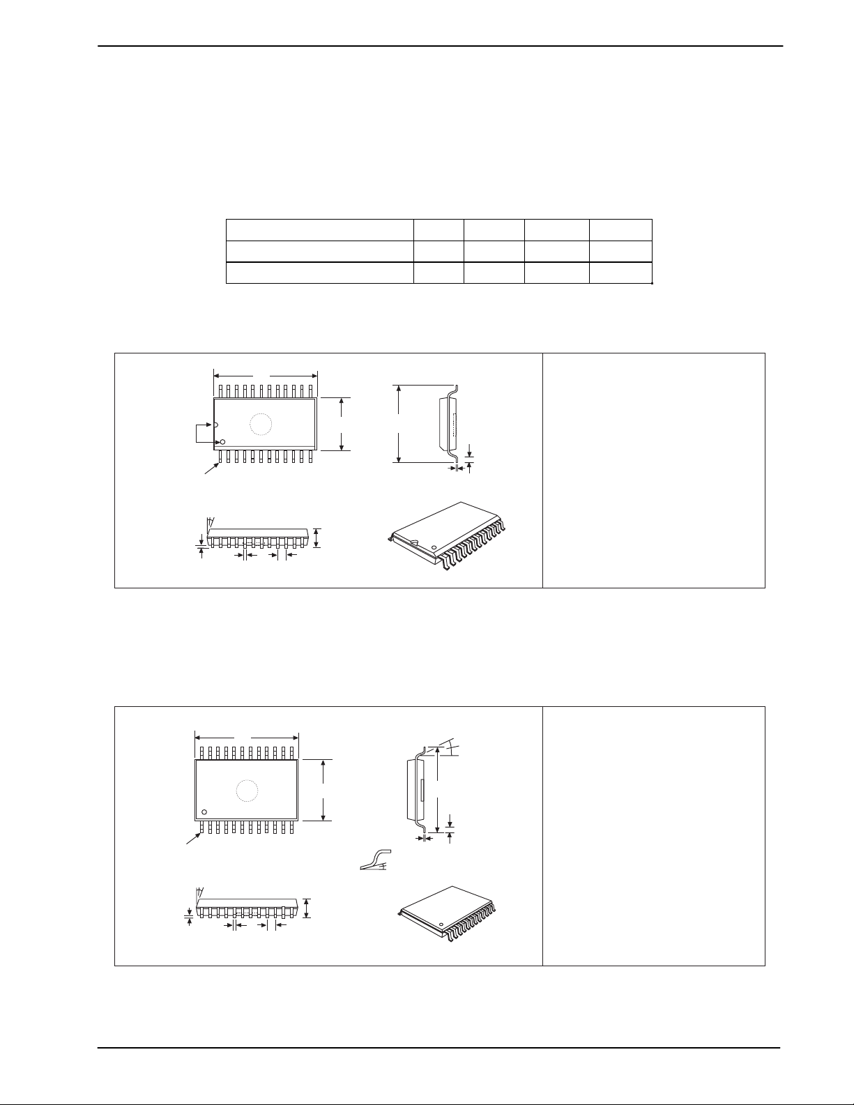
5.2 Packaging
ALTERNATIVE
PIN
LOCA TION
MARKING
PIN 1
H
PackageTolerances
DIM.
A
0.303 (7.70)
B
0.169 (4.30)
C
E
0.248 (6.30)
H
J
0.007 (0.17) 0.012 (0.30)
L
0.020 (0.50)
P
T
0.003 (0.08) 0.008 (0.20)
Y
NOTE: All dimensions in inches (mm.)
0° 8°
Angles are in degrees
PIN 1
H
A
B
E
L
T
Y
C
P
J
Figure 6: 24-pin TSSOP Mechanical Outline: Order as part no. MX465TN
A
B
Z
E
L
T
X
Y
C
P
J
PackageTolerances
DIM.
0.318 (8.07)
A
B
0.205 (5.20)
C
E
0.301 (7.65)
H
J
0.010 (0.25) 0.015 (0.38)
L
0.022 (0.55)
P
T
0.005 (0.13) 0.009 (0.22)
X
Y
Z
NOTE: All dimensions in inches (mm.)
0°
7°
4°
Angles are in degrees
TYP. MAX.MIN.
0.0256 (0.65)
TYP.
0.026 (0.65)
0.311 (7.90)
0.177 (4.50)
0.047 (1.20)----------
0.256 (6.50)
0.006 (0.15)0.002 (0.05)
0.030 (0.75)
MAX.MIN.
0.328 (8.33)
0.213 (5.39)
0.079 (2.00)0.066 (1.67)
0.312 (7.90)
0.008 (0.21)0.002 (0.05)
0.037 (0.95)
8°
9°
10°
Figure 7: 24-pin-SSOP Mechanical Outline:
©1998 MX•COM, INC. www.mxcom.com Tel: 800 638 5577 336 744 5050 Fax: 336 744 5054 Doc. #20480143.008
4800 Bethania Station Road, winston-Salem, NC 27105-1201 USA All trademarks and service marks are held by their respective companies.
Order as part no. MX465DS
Page 15
Low Voltage CTCSS Encoder/Decoder 15 MX465
PackageTolerances
ALTERNATIVE
PIN
LOCA TION
MARKING
A
D
A
B
E
W
PIN 1
X
Y
K
C
H
P
J
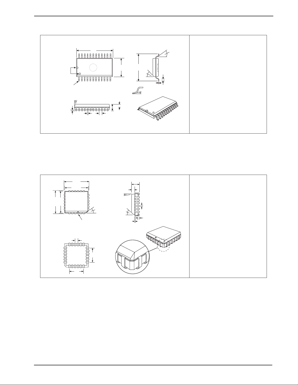
Figure 8: 24-pin SOIC Mechanical Outline:
E
B
C
K
Y
J
H
PIN 1
W
W
T
P
G
F
Z
A
B
C
E
H
L
T
J
K
L
P
T
W
X
Y
Z
NOTE: All dimensions in inches (mm.)
Order as part no. MX465DW
PackageTolerances
A
B
C
D
E
F
G
H
J
K
P
T
W
Y
NOTE: All dimensions in inches (mm.)
TYP. MAX.MIN.DIM.
0.597 (15.16)
0.286 (7.26)
0.093 (2.36)
0.390 (9.90)
0.013 (0.33)
0.036 (0.91)
0.016 (0.41)
0.009 (0.23)
0.050 (1.27)
45°
0°
5°
Angles are in degrees
TYP. MAX.MIN.DIM.
0.380 (9.61)
0.380 (9.61)
0.128 (3.25)
0.417 (10.60)
0.417 (10.60)
0.047 (1.19)
0.049 (1.24)
0.006 (0.152)
30°
0.250 (6.35)
0.250 (6.35)
0.023 (0.58)
45°
Angles are in degrees
5°
6°
0.613 (15.57)
0.299 (7.59)
0.105 (2.67)
0.419 (10.64)
0.020 (0.51)0.003 (0.08)
0.020 (0.51)
0.046 (1.17)
0.050 (1.27)
0.0125 (0.32)
10°
7°
0.409 (10.40)
0.409 (10.40)
0.146 (3.70)
0.435 (11.05)
0.435 (11.05)
0.022 (0.55)0.018 (0.45)
0.048 (1.22)
0.051 (1.30)
0.009 (0.22)
Figure 9: 24-pin PLCC Mechanical Outline:
Order as part no. MX465LH
©1998 MX•COM, INC. www.mxcom.com Tel: 800 638 5577 336 744 5050 Fax: 336 744 5054 Doc. #20480143.008
4800 Bethania Station Road, winston-Salem, NC 27105-1201 USA All trademarks and service marks are held by their respective companies.
Page 16
Low Voltage CTCSS Encoder/Decoder 16 MX465
PIN1
K
K
H
H
L
L
A
B
E1
T
C
K1
P
J
J1
F
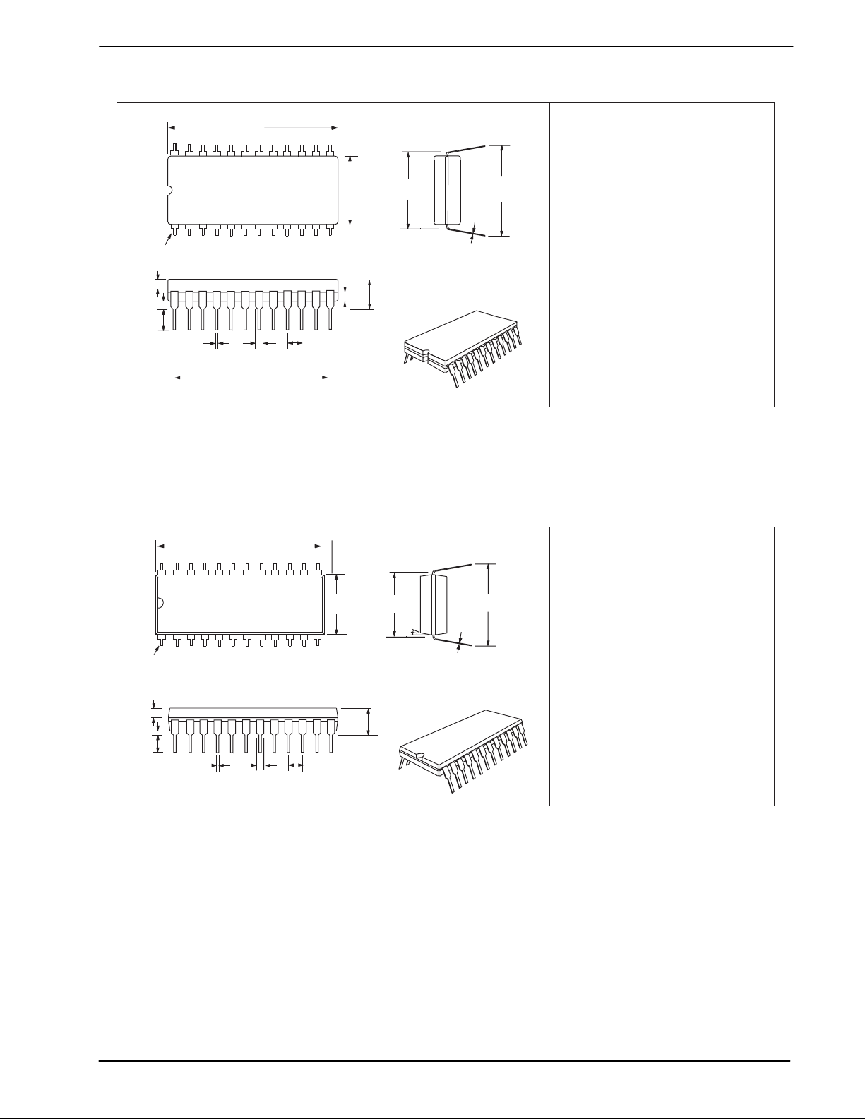
Figure 10: 24-pin-CDIP Mechanical Outline:
PackageTolerances
DIM.
1.240 (31.50)
A
B
E
0.514 (13.06)
C
0.165 (4.19)
E
0.600 (15.23)
E1
0.594 (15.09) 0.615 (15.61)
F
H
J
J1
K
0.050 (1.27)
K1
0.074 (1.88)
L
0.115 (2.92)
P
T
0.0094 (0.239)
NOTE: All dimensions in inches (mm.)
Angles are in degrees
Order as part no. MX465J
TYP. MAX.MIN.
1.260 (32.00)
0.583 (14.79)
0.230 (5.84)
0.670 (17.00)
1.100 (27.94)
0.02 (0.51)
0.018 (0.46)
0.055 (1.39)
0.080 (2.03)
0.080 (2.03)
0.200 (5.08)
0.10 (2.54)
0.0106 (0.269)
PIN1PIN1
K
H
L
AA
BB
E1E1
Y
EE
TT
CC
PP
JJ
J1J1
Figure 11: 24-pin PDIP Mechanical Outline:
PackageTolerances
TYP. MAX.MIN.DIM.
1.200 (30.48)
A
B
0.500 (12.70)
0.151 (3.84)
C
0.600 (15.24)
E
0.590 (14.99) 0.625 (15.88)
E1
0.015 (0.38) 0.045 (1.14)
H
0.015 (0.38) 0.023 (0.58)
J
0.040 (1.02) 0.065 (1.65)
J1
0.066 (1.67) 0.074 (1.88)
K
0.121 (3.07)
L
P
0.008 (0.20) 0.015 (0.38)
T
Y
NOTE: All dimensions in inches (mm.)
0.100 (2.54)
Angles are in degrees
Order as part no. MX465P
1.270 (32.26)
0.555 (14.04)
0.220 (5.59)
0.670 (17.02)
0.160 (4.05)
7°
©1998 MX•COM, INC. www.mxcom.com Tel: 800 638 5577 336 744 5050 Fax: 336 744 5054 Doc. #20480143.008
4800 Bethania Station Road, winston-Salem, NC 27105-1201 USA All trademarks and service marks are held by their respective companies.
Page 17

This datasheet has been download from:
www.datasheetcatalog.com
Datasheets for electronics components.
 Loading...