

Page 1
DATA BULLETIN
MX429A
© 1998 MX-COM Inc. www.mxcom.com Tel: 800 638-5577 336 744-5050 Fax: 336 744-5054 Doc. # 20480128.007
4800 Bethania Station Road, Winston-Salem, NC 27105-1201 USA All trademarks and service marks are held by their respective companies.
1200/2400bps MSK Modem
for Trunked Radio Systems
Features
Band III & General Purpose Trunked Radio
Apps
Full-Duplex 1200 and 2400 Baud Operation
Error Check Word Generation and Checking
Preamble Generation
µProcessor Compatible Interface
Frame SYNC and SYNT
Detection
Low Power Consumption
General Purpose Timer
CARRIER DETECT
TIME CONSTANT
MSK
RECEIVER
RX CARRIER
DETECT
SYNC/SYNT
DETECTOR
BYTE
COUNTER
CHECKSUM
CHECKER
RX DATA
REGISTER
RX DATA
BUFFER
8-BIT uP BUS
8-BIT uP BUS
CLOCKS
CLOCK
GENERATORS
TIMER
CONTROL
REGISTER
TX DATA
BUFFER
TX DATA
REGISTER
BYTE
COUNTER
CHECKSUM
GENERATOR
MSK
TRANSMITTER
INTERRUPT
GENERATOR
DAT A
DAT A
1200/ BAUD2400
V
DD
V
SS
XTAL/CLOCK
XTAL
1.008 MHz
OUTPUT
STROBE
WR/
A1
A0
D7
D6
D5
D4
D3
D2
D1
D0
MICROPROCESSOR
INTERFACE
RECOVERED CLOCK
RX MESSAGE FORMAT
RX CHECKSUM TRUE
V
BIAS
STATUS
REGISTER
SYNC
SYNT
RX DATA READY
RX CARRIER DET.
RX CHECKSUM TRUE
TX DATA READY
TX IDLE
TIMER EXPIRED
TX PARITY
ENABLE
TRANSMITTER
OUTPUT
IRQ
RX DATA RDY
TX DATA RDY
SYNC
SYNT
TX IDLE
RX ENABLE
TX ENABLE
RX MESSAGE FORMA T
TX PARITY ENABLE
RECEIVER INPUT
The MX429A is a single-chip CMOS 1200 and 2400 baud MSK modem, designed primarily for use in Trunked
Radio Systems but may also be employed in other general purpose radio or line data communication
applications. The device has been designed to conform to the UK Band III trunked radio protocols MPT
1317/1327.
The MX429A is full duplex at 1200 and 2400 baud and includes an 8-bit parallel microprocessor interface and
a programmable timer which may be set for interrupt periods of 8 to 120 bits. Preamble may be generated by
the device in transmit. The 16-bit SYNC or SYNT words are detected in receive. An error check word is
automatically generated in transmit and error checking is performed in the receive mode. An on-chip
Xtal/clock generator requiring an external 4.032MHz Xtal or clock input provides both 4.032MHz and
1.008MHz outputs and performs all modem timings.
The MX429A requires a single 5-volt power supply, has a powersave facility, and is available in the following
package styles: 24-pin CDIP (MX429AJ), 24-pin PDIP (MX429AP), and 24-pin PLCC (MX429ALH).
Page 2

1200/2400bps MSK Modem for Trunked Radio Systems 2 MX429A
© 1998 MX-COM Inc. www.mxcom.com Tel: 800 638-5577 336 744-5050 Fax: 336 744-5054 Doc. # 20480128.007
4800 Bethania Station Road, Winston-Salem, NC 27105-1201 USA All trademarks and service marks are held by their respective companies.
CONTENTS
Section Page
1 Block Diagram.................................................................................................................3
2 Signal List........................................................................................................................3
3 External Components.....................................................................................................5
4 General Description........................................................................................................6
4.1 Modems in Mobile Data Signaling.......................................................................................... 6
4.1.1 Digital Code Format....................................................................................................................6
4.1.2 Operation....................................................................................................................................6
4.1.3 Non MPT Application – Full-Duplex..........................................................................................7
4.1.4 Control Register (A1 = 1, A0 = 1,
WR/
= 0, Write Only)...........................................................7
4.1.5 Status Register (A1 = 1, A0 = 1,
WR/
= 1, Read Only)............................................................8
4.1.6 Rx Data Buffer (A1 = 1, A0 = 0,
WR/
= 1, Read Only).............................................................9
4.1.7 Tx Data Buffer (A1 = 1, A0 = 0,
WR/
= 0, Write Only)..............................................................9
4.2 Syndrome Word.................................................................................................................... 10
4.2.1 Syndrome Low Byte (A1 = 0, A0 = 0,
WR/
= 1, Read Only) ..................................................10
4.2.2 Syndrome High Byte (A1 = 0, A0 = 1,
WR/
= 1, Read Only)..................................................10
4.3 Carrier Detect Time Constant............................................................................................... 10
5 Application ....................................................................................................................11
5.1 Checksum Generation and Checking................................................................................... 11
5.2 Receive Operation................................................................................................................ 11
5.3 Transmit Operation............................................................................................................... 12
5.4 Basic Power Up Software..................................................................................................... 13
5.5 Basic Software Interrupt Flow............................................................................................... 14
5.6 Bus Interface Timing............................................................................................................. 15
5.6.1 Bus interface design migration from MX429 to MX429A..........................................................15
6 Performance Specification...........................................................................................15
6.1 Electrical Performance ......................................................................................................... 15
6.1.1 Absolute Maximum Ratings......................................................................................................15
6.1.2 Operating Limits .......................................................................................................................15
6.1.3 Operating Characteristics.........................................................................................................16
6.1.4 Timing.......................................................................................................................................18
6.2 Packaging............................................................................................................................. 18
MX•COM, Inc. reserves the right to change specifications at any time and without notice.
Page 3
1200/2400bps MSK Modem for Trunked Radio Systems 3 MX429A
© 1998 MX-COM Inc. www.mxcom.com Tel: 800 638-5577 336 744-5050 Fax: 336 744-5054 Doc. # 20480128.007
4800 Bethania Station Road, Winston-Salem, NC 27105-1201 USA All trademarks and service marks are held by their respective companies.
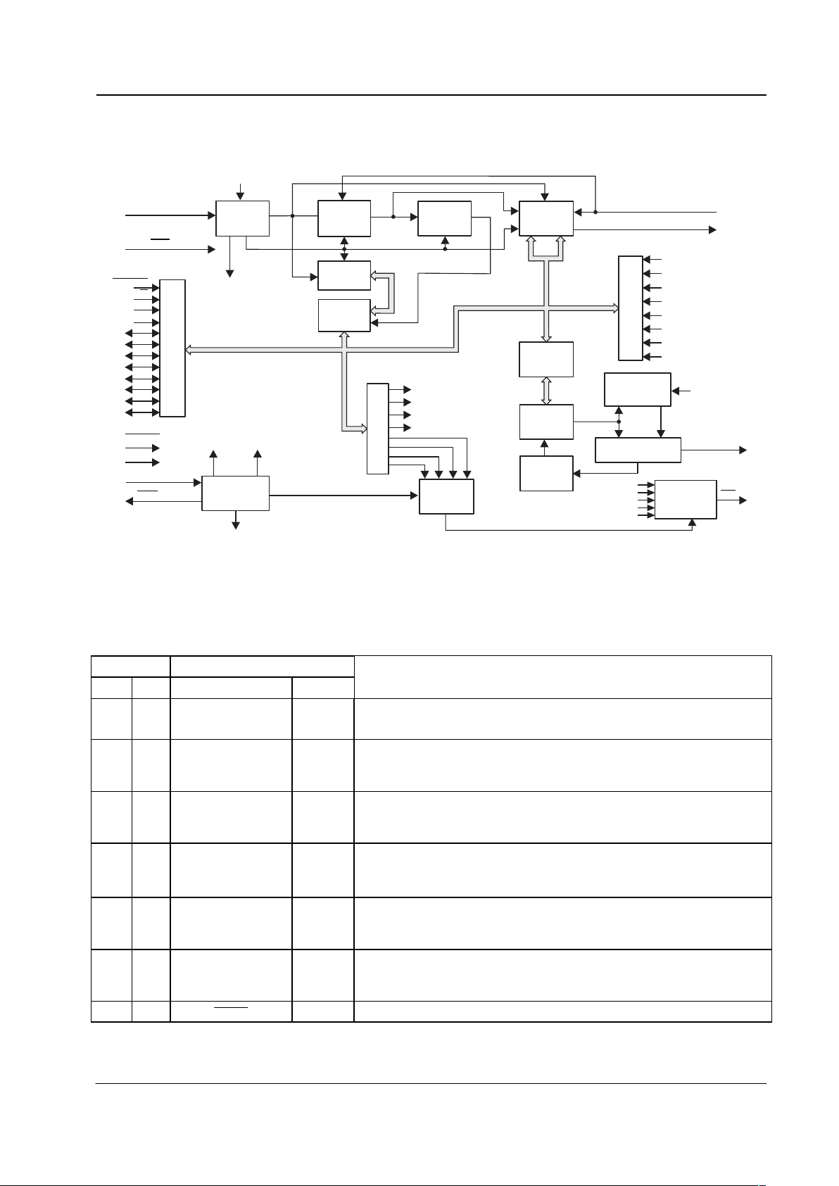
1 Block Diagram
CARRIER DETECT
TIME CONSTANT
MSK
RECEIVER
RX CARRIER
DETECT
SYNC/SYNT
DETECTOR
BYTE
COUNTER
CHECKSUM
CHECKER
RX DATA
REGISTER
RX DATA
BUFFER
8-BIT uP BUS
8-BIT uP BUS
CLOCKS
CLOCK
GENERA TORS
TIMER
CONTROL
REGISTER
TX DATA
BUFFER
TX DATA
REGISTER
BYTE
COUNTER
CHECKSUM
GENERA TOR
MSK
TRANSMITTER
INTERRUPT
GENERA TOR
DAT A
DAT A
1200/ BAUD2400
V
DD
V
SS
XT AL/CLOCK
XT AL
1.008 MHz
OUTPUT
STROBE
WR/
A1
A0
D7
D6
D5
D4
D3
D2
D1
D0
MICROPROCESSOR
INTERFACE
RECOVERED CLOCK
RX MESSAGE FORMAT
RX CHECKSUM TRUE
V
BIAS
ST ATUS
REGISTER
SYNC
SYNT
RX DATA READY
RX CARRIER DET.
RX CHECKSUM TRUE
TX DATA READY
TX IDLE
TIMER EXPIRED
TX P ARITY
ENABLE
TRANSMITTER
OUTPUT
IRQ
RX DAT A RDY
TX DAT A RDY
SYNC
SYNT
TX IDLE
RX ENABLE
TX ENABLE
RX MESSAGE FORMAT
TX PARITY ENABLE
RECEIVER INPUT
Figure 1: Block Diagram
2 Signal List
Pin No. Signal Description
J/P LH Name Type
11 V
BIAS
The internal circuitry bias line, held at VDD/2 this pin must be
decoupled to V
SS
by a capacitor, see Figure 2.
2 2 Transmit Output Output The 1200 baud, 1200Hz/1800Hz and 2400 baud, 1200Hz/2400Hz
MSK Tx output. When not enabled by the Control Register (D0) its
output impedance is set high.
3 4 Receiver Input Input The 1200/2400 baud received MSK signal input. The
1200Hz/1800Hz, 1200Hz/2400Hz audio to this pin must be ac
coupled via a capacitor, see Figure 2.
55 V
DD
Power Positive Supply. A single +5V regulated supply is required. It is
recommended that this power rail be decoupled to V
SS
by a
capacitor, see Figure 2.
6 6 Carrier Detect
Time Constant:
The on-chip Carrier Detect function requires external
component(s) on this pin. See Figure 2for recommended
component(s).
7 7 Xtal/Clock The input to the clock oscillator inverter. A 4.032 MHz Xtal or
externally derived clock pulse input should be connected here,
see Figure 2.
88
XTAL
The output of the 4.032 MHz clock oscillator.
Page 4
1200/2400bps MSK Modem for Trunked Radio Systems 4 MX429A
© 1998 MX-COM Inc. www.mxcom.com Tel: 800 638-5577 336 744-5050 Fax: 336 744-5054 Doc. # 20480128.007
4800 Bethania Station Road, Winston-Salem, NC 27105-1201 USA All trademarks and service marks are held by their respective companies.
Pin No. Signal Description
J/P LH Name Type
99 D0
10 10 D1
11 11 D2 Microprocessor Data Interface
12 12 D3 These 8 lines are used by the device to communicate with a
micro-
13 13 D4
processor with the R/
W , A0 and A1 inputs determining register
selection.
14 14 D5
15 15 D6
16 16 D7
17 17 A0
Register Selection: These inputs, with the R/
W input, select the
18 18 A1 required register to the data bus as shown in Table 2
19 19
STROBE
Performs the dual functions of selecting the device for Read or
Write and strobing data in or out. It should be generated by gating
the high order address bits with a Read/Write clock. The MX429A
is selected when this pin is a logic ‘0’.
20 20
R/
W
Used in conjunction with A1 and A0 to determine which internal
registers are connected to the data interface pins (D0 to D7)
during Strobe.
21 21
IRQ
Interrupt Request. This line will go to a logic '0' when an interrupt
occurs. This output can be "wire OR'd" with other active low
components (100kW pullup to V
DD
). The conditions that cause
the interrupts are indicated at the Status Register and are as
follows: Timer Expired, Rx Data Ready, Tx Data Ready, Tx Idle,
Rx SYNC Detect, Rx SYNT Detect
22 24
Baud 2400/1200
Select
A logic ‘1’ on this pin selects the 1200 baud option. Tone
frequencies are: one cycle of 1200Hz represents a logic ‘1’, one
and a half cycles of 1800Hz represents a logic ‘0’.
A logic ‘0’ on this pin selects the 2400 baud option. Tone
frequencies are: one half cycle of 1200Hz represents a logic ‘1’,
one cycle of 2400Hz represents a logic ‘0’. This pin has an
internal 1M pullup resistor.
23 22 V
SS
Power Negative Supply (GND)
24 23 Clock/4 A 1.008 MHz (X1 ÷ 4) clock is available at this output for external
circuit use, note the source impedance and source current limits.
4 3 Leave this pin open-circuit
Table 1: Signal List
Register R/
W
A0 A1
Control 0 1 1
Status 1 1 1
Rx Data 1 0 1
Tx Data 0 0 1
Syndrome Low 1 0 0
Syndrome High 1 1 0
Table 2: Register Selection
Page 5
1200/2400bps MSK Modem for Trunked Radio Systems 5 MX429A
© 1998 MX-COM Inc. www.mxcom.com Tel: 800 638-5577 336 744-5050 Fax: 336 744-5054 Doc. # 20480128.007
4800 Bethania Station Road, Winston-Salem, NC 27105-1201 USA All trademarks and service marks are held by their respective companies.
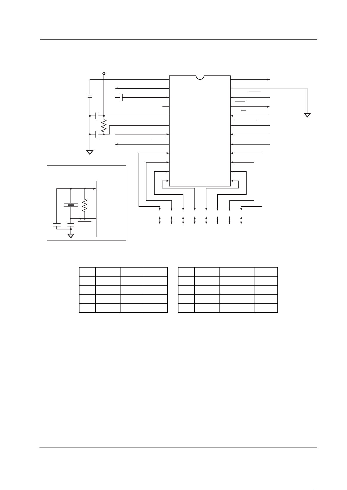
3 External Components
MICROPROCESSOR DATA INTERFACE
D0
D1 D2
D3
D4
D4
D5D5D6
D6
D7
D7
A0
A1
V
DD
V
DD
C4
C6
C5
C3
TRANSMIT OUTPUT
RECEIVE INPUT
'CD' TIME CONSTANT
XTAL/CLOCK
CLOCK/4
1200/ BAUD SELECT2400
R2
V
BIAS
V
SS
C1
C2
X1
R1
Xtal/Clock
MX429A
XTAL
7
8
Recommended Xtal
Component
24
23
22
21
20
19
18
17
16
15
14
13
D0
D1
D2
D3
XTAL
1
2
3
4
5
6
7
8
9
10
11
12
STROBE
R/W
IRQ
Figure 2: Recommended External Components
R1
1M
10%
C4
1.0F
20%
R2
1M
10%
C5
1.0F
20%
C1 33pF
20%
C6
1.0F
20%
C2 33pF
20%
C3
0.1F
20%
X1 Note 1 4.032MHz
Table 3: Recommended External Components
Notes:
1. For best results, a crystal oscillator design should drive the clock inverter input with signal levels of at
least 40% of VDD, peak to peak. Tuning fork crystals generally cannot meet this requirement. To
obtain crystal oscillator design assistance, consult your crystal manufacturer.
Page 6

1200/2400bps MSK Modem for Trunked Radio Systems 6 MX429A
© 1998 MX-COM Inc. www.mxcom.com Tel: 800 638-5577 336 744-5050 Fax: 336 744-5054 Doc. # 20480128.007
4800 Bethania Station Road, Winston-Salem, NC 27105-1201 USA All trademarks and service marks are held by their respective companies.
4 General Description
4.1 Modems in Mobile Data Signaling
4.1.1 Digital Code Format
The MPT 1327 Signaling Standard for Trunked LMR Systems protocol is used by the MX429 for
communication between a Trunking System Controller (TSC) and users' radio units. These data stream
formats are summarized in Figure 3.
Preamble SYNC or SYNT
For bit sync. SYNC Word Address Code
101010...10..- bit reversals 1100010011010111 Word Optional Data
Minimum 16 bits, ending in SYNT Word Code Words
logic'0' 0011101100101000 64 Bits
Address Code Word Structure
(Bit number 1 is transmitted first)
Bit No.
No.of Bits
Bit Name
1
1
Logic '1'
2 to 8
7
User Identity
9 to 48
40
Address
&
Data
49 to 64
16
Check Bits
(Checksum)
Figure 3: Tx and Rx Data Stream
4.1.2 Operation
The MX429A can be used for Full-Duplex operation with the host microprocessor only having to operate on
the data while the modem (MX429A) handles all other signaling routines and requirements.
In the Tx mode the MX429A will :
1. Internally generate and transmit a preamble – bit reversals, for system bit synchronization.
2. Accept from the host, and transmit, a 16-bit 'SYNC' or 'SYNT' word.
3. Accept from the host, and transmit, 6 bytes of data (Address Code Word):
A. Upon a software command, internally calculate and transmit a 2-byte checksum based on the
previous 6 data bytes.
B. Upon a software command, disable internal checksum generation and allow continuous data
transmission.
4. Transmit 1 'hang bit' and go idle when all loaded data traffic has been sent (followed by a "Tx Idle"
interrupt).
In the Rx mode the MX429A will:
1. Detect and achieve bit synchronization within 16 bits.
2. Search for and detect the 16-bit 'SYNC'/'SYNT' word.
3. Output all received data after 'SYNC/SYNT,' in byte form.
4. Upon a software command (Rx Message Format), use the received checksum to calculate the
presence (if any) of errors, and advise the host with an interrupt and a 16-bit Syndrome word.
Note: In Rx, a software command is used to determine whether a 'SYNC'/'SYNT' word is required after
every 8 (6 data + 2 checksum ) received bytes, or "data" is received continually.
Normally the 'SYNC' word is used on the Control data channel and the 'SYNT' word is used on the
Traffic data channel.
Page 7

1200/2400bps MSK Modem for Trunked Radio Systems 7 MX429A
© 1998 MX-COM Inc. www.mxcom.com Tel: 800 638-5577 336 744-5050 Fax: 336 744-5054 Doc. # 20480128.007
4800 Bethania Station Road, Winston-Salem, NC 27105-1201 USA All trademarks and service marks are held by their respective companies.
4.1.3 Non MPT Application – Full-Duplex
The functions described in this section, to allow the MX429A modem to operate as a general purpose device,
are obtained using the commands and indications detailed in the “Register Instructions” pages.
Tx: When enabled the device transmits a “101010......10” preamble until data for transmission is loaded by
the host microprocessor. Transmits 6 bytes of the loaded data followed by a 2-byte checksum based on
that data. As long as Tx data is loaded the transmitter will transmit, the 2-byte checksum being produced
after every 6 bytes (8 byte packages). Automatic checksum generation can be inhibited by a software
command to allow transmission of continuous data streams.
Rx: When enabled requires the 16-bit SYNC or SYNT word (see notes) before outputting data bytes. The
modem receiver will then output continuous bytes of data, after every 6 bytes received a 2-byte
checksum word will be output and can be ignored or used for error checking.
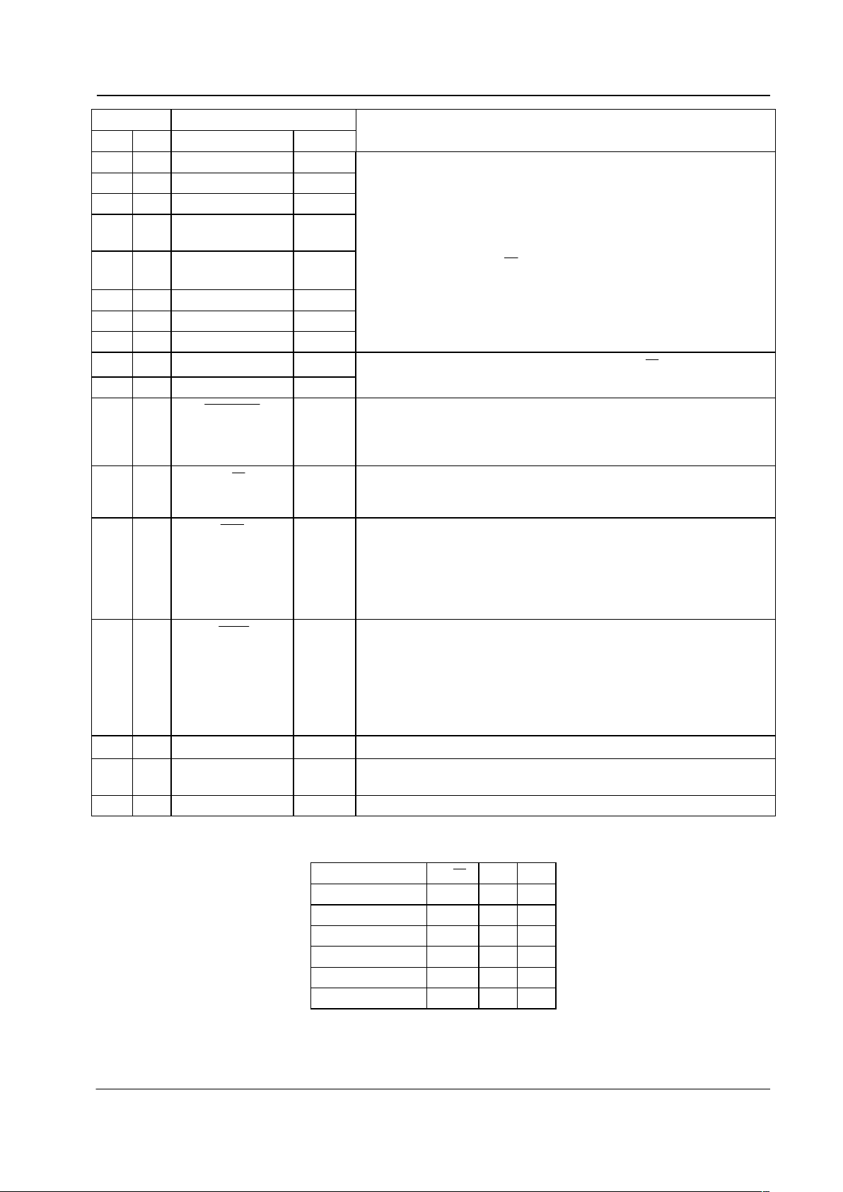
4.1.4 Control Register (A1 = 1, A0 = 1,
WR/
= 0, Write Only)
The Control Register, when selected, directs the modem’s operation as described in Table 4
Bit Description Function
Bit 0
D0
TX Enable
Set
: D0 enables the transmitter for operation. A '0 – 1' transition causes bit
synchronization and the start of 1010.........10 preamble pattern transmission. At least
one byte of preamble will be transmitted. If data is loaded into the Tx Data Buffer before
one byte has been sent then that data will follow, otherwise whole bytes of preamble will
continue until data is loaded.
Clear
: The Transmitter Output pin is set to a high impedance and no transmitter
interrupts are produced.
Bit 1
D1
Tx Parity
Enable
Set
: D1 indicates to the transmitter that 2–byte checksums are to be generated by the
modem. A '0 – 1' transition starts checksum generation on the next six bytes loaded
from the Tx Data Buffer into the Tx Data Register. Checksum generation continues for
every 6 bytes loaded until this bit is cleared. The transmitter will send the generated
checksum (2 bytes) after the last of each 6 bytes have been sent. If an underrun (no
more data loaded) condition occurs before 6 bytes have been loaded checksum
generation will abort, the transmission will cease after one 'hang' bit has been sent and
Bit 4 in the Status Register (Tx Idle) will be set. No checksum will be transmitted.
Clear
: No checksum generation is carried out and the host may supply the checksum
bytes. The output is then “as written”.
Bit 2
D2
Rx Enable
Set
: D2 enables the receiver for operation. No data is produced (i.e. No Rx Data
Ready interrupts) until a 'SYNC' or 'SYNT' word is found in the received bit stream.
Clear
: The receiver is disabled and all interrupts caused by the receiver are inhibited.
Bit 3
D3
Rx Message
Format
Set
: D3 is sampled after a checksum has been received and allows the host to control
the way the receiver handles the following data bits. If 'set' the receiver will assume that
the next 6 bytes are data and will start error checking accordingly.
Clear
: The receiver will stop data transfer to the host after the 2 checksum bytes until
another 'SYNC' or 'SYNT' frame word is received.
Bit 4
D4
Timer LSB
Bit 5
D5
Timer Reference Table 5
Bit 6
D6
Timer
Bit 7
D7
Timer MSB If a new timer value is written to these inputs within 1 byte period of the last timer
interrupt then the next timer period will be correct without first having to reset the timer,
otherwise the timer must be reset to zero and then set to the new time.
Tx Enable
If using the internal Tx preamble generation facility, e.g. with the internal timer setting
the preamble length, the device may occasionally produce a Tx Ready interrupt
immediately after a Tx Enable command. User software should handle this occurrence
by either:
a. Detecting that the timer interrupt status bit is not set and that it is not appropriate to
load Tx data at this time.
b. Not using the timer. i.e. immediately after Tx Enable, reading the Status Register and
loading a byte of preamble. This resets any interrupt. The length of preamble
transmitted is now controlled by the number of bytes loaded.
Page 8

1200/2400bps MSK Modem for Trunked Radio Systems 8 MX429A
© 1998 MX-COM Inc. www.mxcom.com Tel: 800 638-5577 336 744-5050 Fax: 336 744-5054 Doc. # 20480128.007
4800 Bethania Station Road, Winston-Salem, NC 27105-1201 USA All trademarks and service marks are held by their respective companies.
Table 4: Control Register
D7 D6 D5 D4 Reset counter and disable timer interrupts
0 0 0 0 Count and interrupt every
0001“““8 bits
0010"""16 bits
0011"""24 bits
0100"""32 bits
0101"""40 bits
0110"""48 bits
0111"""56 bits
1000"""64 bits
1001"""72 bits
1010"""80 bits
1011"""88 bits
1100"""96 bits
1 1 0 1 " " " 104 bits
1 1 1 0 " " " 112 bits
1 1 1 1 " " " 120 bits
Table 5: Timer Control Bits
4.1.5 Status Register (A1 = 1, A0 = 1,
WR/
= 1, Read Only)
When an interrupt is generated, the
IRQ
Output goes low with the Status Register bits indicating the sources
of the interrupt.
Bit Description Function
Bit 0
D0
Rx Data
Ready
D0
: when set, causes an interrupt indicating that received data is ready to be read
from the Rx Data Buffer. This data must be read within 8 bit periods.
Set
when a byte of data is loaded into the Rx Data Buffer, if a frame (SYNC/SYNT)
word has been received.
Bit and Interrupt Cleared
:
(i). by a read of the Status Register followed by a read of the Rx Data Buffer
(ii). by Rx Enable going Low.
Bit 1D1Rx Checksum
True
D1
: when set, indicates that the error checking on the previous 6 bytes agreed with the
received checksum. This function, which is valid when the Rx Data Ready bit (D0) is
set for the second byte of the received checksum, does not cause an interrupt.
Set
: by a correct comparison between the received and generated checksums.
Cleared
:
(i). by a read of the Status Register followed by a read of the Rx Data Buffer
(ii). by Rx Enable going Low.
Bit 2
D2
Rx Carrier
Detect
D2
: is a “Real Time” indication from the modem receiver's carrier detect circuit and
does not cause an interrupt. When MSK tones are present at the receiver input this bit
goes High, for no MSK input this bit goes Low. When the Rx Enable bit (D2– Control
Register) is Low Rx Carrier Detect will go Low.
Bit 3
D3
Tx Data
Ready
D3: when set, causes an interrupt to indicate that a byte of data should be written to
the Tx Data Buffer within 8 bit periods.
Set
:
(i). when the contents of the Tx Data Buffer are transferred to the Tx Data Register
(ii). when the Tx Enable is set (No interrupt is generated in this case.
Bit Cleared
:
(i). by a read of the Status Register followed by a write to the Tx Data Buffer
(ii). by Tx Enable going Low.
Interrupt Cleared
:
Page 9

1200/2400bps MSK Modem for Trunked Radio Systems 9 MX429A
© 1998 MX-COM Inc. www.mxcom.com Tel: 800 638-5577 336 744-5050 Fax: 336 744-5054 Doc. # 20480128.007
4800 Bethania Station Road, Winston-Salem, NC 27105-1201 USA All trademarks and service marks are held by their respective companies.
Bit Description Function
(i). by a read of the Status Register
(ii). by Tx Enable going Low.
Bit 4
D4
Tx Idle
D4
: causes an interrupt when set, to indicate that all loaded data and one 'hang' bit
have been transmitted.
Set
: one bit period after the last byte is transmitted. This last byte could be either
“checksum” or “ loaded data” depending upon the Tx Parity Enable state (Control
Register D1).
Bit Cleared
:
(i). by a write to the Tx Data Buffer
(ii). by Tx Enable going Low.
Interrupt Cleared
:
(i). by a read of the Status Register
(ii). by Tx Enable going Low.
Bit 5D5Timer Interrupt
D4
: causes an interrupt when set, to indicate that all loaded data and one 'hang' bit
have been transmitted.
Set
: one bit period after the last byte is transmitted. This last byte could be either
“checksum” or “ loaded data” depending upon the Tx Parity Enable state (Control
Register D1).
Bit Cleared
:
(i). by a write to the Tx Data Buffer
(ii). by Tx Enable going Low
Interrupt Cleared
:
(i). by a read of the Status Register
(ii). by Tx Enable going Low.
Bit 6
D6
Rx SYNC
Detect *
D6
: when set, causes an interrupt to indicate that a 16-bit 'SYNC' word
(1100010011010111) has been detected in the received bit stream.
Set
: on receipt of the 16th bit of a 'SYNC' word.
Bit and Interrupt Cleared
:
(i). by a read of the Status Register
(ii). by Rx Enable going Low.
Bit 7
D7
Rx SYNT
Detect *
D7
: when set, causes an interrupt to indicate that a 16-bit 'SYNT' word
(0011101100101000 ) has been detected in the received bit stream.
Set
: on receipt of the 16th bit of a 'SYNT' word.
Bit and Interrupt Cleared
:
(i). by a read of the Status Register
(ii). by Rx Enable going Low.
* SYNC and SYNT Detection is disabled while the checksum checker is running.
Table 6: Status Register
4.1.6 Rx Data Buffer (A1 = 1, A0 = 0,
WR/
= 1, Read Only)
These 8 bits are the last byte of data received with bit 7 being received first. Note the relative positions of the
MSB and LSB presented in this bit stream, the position may be different to the convention used in other
µProcessor peripherals.
D0
LSB
D1 D2 D3 D4 D5 D6 D7
MSB
4.1.7 Tx Data Buffer (A1 = 1, A0 = 0,
WR/
= 0, Write Only)
These 8 bits loaded to the Tx Data Buffer are the next byte of data that will be transmitted, with bit 7 being
transmitted first. Note the relative positions of the MSB and LSB presented in this bit stream, the position may
be different to the convention used in other µProcessor peripherals. If the Tx Parity Enable bit (Control
Register D1 ) is set, a 2–byte checksum will be inserted and transmitted by the modem after every 6
transmitted “message” bytes.
D0
LSB
D1 D2 D3 D4 D5 D6 D7
MSB
Page 10

1200/2400bps MSK Modem for Trunked Radio Systems 10 MX429A
© 1998 MX-COM Inc. www.mxcom.com Tel: 800 638-5577 336 744-5050 Fax: 336 744-5054 Doc. # 20480128.007
4800 Bethania Station Road, Winston-Salem, NC 27105-1201 USA All trademarks and service marks are held by their respective companies.
4.2 Syndrome Word
This 16-bit word (both Low and High bytes) may be used to correct errors. Bits S1 to S15 are the 15 bits
remaining in the polynomial divider of the checksum checker at the end of 6 bytes of “ received message.”
For a correct message all 15 bits (S1 to S15) will be zero. The 2 Syndrome bytes are valid when the Rx Data
Ready bit (Status Register D0) is set for the second byte of the received checksum and should be read, if
required, before 8 byte periods.
4.2.1 Syndrome Low Byte (A1 = 0, A0 = 0,
WR/
= 1, Read Only)
D0S1D1S2D2S3D3S4D4S5D5S6D6S7D7
S8
4.2.2 Syndrome High Byte (A1 = 0, A0 = 1,
WR/
= 1, Read Only)
D0S9D1
S10D2S11D3S12D4S13D5S14D6S15D7Parity Error
D7
: This is a “Parity Error Bit”. Indicating an error between the received parity bit and the parity bit internally
generated from the incoming message. Therefore a correctly received message all 16 bits of the Syndrome
Word
(S1 to S15 and Parity Error) will be zero.
4.3 Carrier Detect Time Constant
The value of the Carrier Detect capacitor, C5, determines the carrier detect time constant. A long time
constant (larger value C5) results in improved noise immunity but increased response time. C5 may be varied
to optimize noise immunity/response time.
1. With R2 = 1M and C5 = 1µF as external components for the carrier detect function at 1200 baud
only.
2. By using C5 = 0.1µF and removing R2 completely the MX429A will operate at both 1200 and 2400
baud rates.
109876543210
2
3
4
6
8
10
-5
10
-4
10
-3
10
-2
Ideal Coherent MSK
Characteristic
Bit Error Rate
(Logarithmic Scale)
Signal to Noise Ratio (dB) [Bit-Rate Bandwidth]
(Linear Scale)
MX429A
Characteristic
2x10
-2
11 12 13 14 15 16
Figure 4: Bit Error Rate vs. Signal to Noise Ratio
Page 11

1200/2400bps MSK Modem for Trunked Radio Systems 11 MX429A
© 1998 MX-COM Inc. www.mxcom.com Tel: 800 638-5577 336 744-5050 Fax: 336 744-5054 Doc. # 20480128.007
4800 Bethania Station Road, Winston-Salem, NC 27105-1201 USA All trademarks and service marks are held by their respective companies.
5 Application
5.1 Checksum Generation and Checking
Generation – The checksum generator takes the 48 bits from the 6 bytes loaded into the Tx Data Buffer and
divides them modulo–2, by the generating polynomial;-
X15 + X14 + X13 + X11 + X4 + X2 + 1
It then takes the 15-bit remainder from the polynomial divider, inverts the last bit and appends an EVEN parity
bit generated from the initial 48 bits and the 15 bit remainder (with the last bit inverted). This 16–bit word is
used as the "Checksum."
Checking – The checksum checker does two things:
It takes the first 63 bits of a received message, inverts bit 63, and divides them modulo–2, by the generating
polynomial;-
X15 + X14 + X13 + X11 + X4 + X2 + 1
The 15 bits remaining in the polynomial divider are checked for all zero. Secondly, it generates an EVEN
parity bit from the first 63 bits of a received message and compares this bit with the received parity bit (bit 64).
If the 15 bits in the polynomial divider are all zero, and the two parity bits are equal, then the Rx Checksum
True bit (SR D1) bit is set.
5.2 Receive Operation
Rx ENABLE
Where SYNC/SYNT is requiredafter every message
Rx INPUT
IRQ OUTPUT
Rx DATA
READY
READ STATUS
REGISTER
SYNC (SYNT)
DETECT
Rx CHECKSUM
TRUE
READ Rx
DATA BUFFER
Rx MESSAGE
FORMAT
SYNC SYNC A1 A2 A3
SYNC
A5 A6 C1 C2SYNCSYNCA1A2A3A4A5A6C1C2
A1 A2 A3 A4 A5 A6 C1 C2A1 A2 A3 A4 A5 A6 C1 C2
Where additional data will follow the initial address data, indicated by the state of the Rx Message Format bit
D1
D3 D4 D5 D6 C1 C2 D1
Note: A- Address, C - Checksum, D - Datacode
{additional DataWords}
SYNC SYNC A1 A2 A5 A6 C1 C2
D2
Rx INPUT
IRQ OUTPUT
Rx DA TA
READY
READ STATUS
REGISTER
SYNC (SYNT)
DETECT
Rx CHECKSUM
TRUE
READ Rx
DATA BUFFER
Rx MESSAGE
FORMAT
A3 A4
MODE 2
MODE 1
A4
D1 D2 D2 D4 D5 D6 C1 C2
A1
A4
A5 A6
C1 C2
A2
A3
Rx Message Format issampled at this point to decide,
(a) whether the message is completeor (b), more datafollows
Figure 5: Receive Operation
Page 12

1200/2400bps MSK Modem for Trunked Radio Systems 12 MX429A
© 1998 MX-COM Inc. www.mxcom.com Tel: 800 638-5577 336 744-5050 Fax: 336 744-5054 Doc. # 20480128.007
4800 Bethania Station Road, Winston-Salem, NC 27105-1201 USA All trademarks and service marks are held by their respective companies.
5.3 Transmit Operation
Tx ENABLE
Tx ENABLE
Tx ENABLE
(a) Tx - one messagewith checksum supplied by host
(b) Tx - one messagewith checksum generatedinternally
(c) Tx - more thanone message ,with checksumgenerated internally
Tx INPUT
Tx INPUT
Tx INPUT
Tx INPUT
Tx IDLE
Tx IDLE
Tx IDLE
Tx Parity Enable remains 'High'- indicating that
all following data is to be includedin the checksum
Tx Parity Enable is 'Low' - indicatingthat the
SYNC/SYNT word is not to be included in the
next checksum
IRQ OUTPUT
IRQ OUTPUT
IRQ OUTPUT
IRQ OUTPUT
Tx DATA
READY
Tx DATA
READY
Tx DATA
READY
Tx DATA
READY
WRITE TO Tx
DA TA BUFFER
WRITE TO Tx
DA TA BUFFER
WRITE TO Tx
DA TA BUFFER
WRITE TO Tx
DA TA BUFFER
Tx PARITY
ENABLE
Tx PARITY
ENABLE
Tx PARITY
ENABLE
Tx PARITY
ENABLE
READ STATUS REGISTER
READ STATUS REGISTER
READ STATUS REGISTER
READ STATUS
REGISTER
S1
S1
S1 S1S1
D1
S2
S2
S2 S2
D2
A1
A1
A1 A1
D3
A2
A2
A2 A2
D4
A3
A3
A3 A3
D5
A4
A4
A4 A4
D6
A5
A5
A5 A5
A6
A6
A6 A6
C1 C2
S1S1S2S2A1A1A2A2A3A3A4A4A5A5A6A6C1C1C2
C2 H
H
(1)
(1)
(2)
(2)
(2)
(2)
(2)
(3)
(3)
Pn
Pn
P2
P2
P1
P1 P2 Pn S1 S2 A1 A2 A3 A4 A5 A6A6C1C1C2C2S1
D1
S1S2D2A1D3A2D4A3D5A4D6A5C1A6C2C1HC2
P1
Notes:
A - Address Code
C - Checksum
D - Data Code
H - Hang Bit
P - Preamble
S - SYNC/SYNT
(1) - Tx Output at bias level
(2) - Tx Output at High Impedance
(3) - If Tx Data Ready is Set here, it inhibits Tx Data Ready
Interrupt -TheTx Idle Interrupt occurs 1 b it late r
Figure 6: Transmit Operation
Page 13

1200/2400bps MSK Modem for Trunked Radio Systems 13 MX429A
© 1998 MX-COM Inc. www.mxcom.com Tel: 800 638-5577 336 744-5050 Fax: 336 744-5054 Doc. # 20480128.007
4800 Bethania Station Road, Winston-Salem, NC 27105-1201 USA All trademarks and service marks are held by their respective companies.
5.4 Basic Power Up Software
Set up a 1 byte variable - initialise to zero
(Rx Msg Length)
Set up an 8 byte buffer
start address - (Rx Buffer)
Set up a 1 byte variable - initialise to zero
(Tx Msg Sent)
Set up an 8 byte variable
start address - (Tx Buffer)
Put message for transmission into
buffer[Tx Buffer]
Write to ControlRegister
Bit0 -Tx Enable = '1'
Bit1 - Tx Parity Enable = '0'
Wait 1 byte
(Specification requires a minimum of
two bytes preamble)
Write to ControlRegister
Bit2 - Rx Enable = '1'
Bit3 - Rx Message Format = '0'
Write [Tx Buffer{ }]
to
Tx Data Buffer
Ø
Write 04 to ControlRegister
- Wait at least 1 bit-
Enable microprocessor interrupts
Write zeros to MX 429A Control
Register
T ransm it Receive
Receive
or
T ransm it?
Power Up
Return to Main Pro gram
Figure 7: Basic Power-Up Software
Page 14

1200/2400bps MSK Modem for Trunked Radio Systems 14 MX429A
© 1998 MX-COM Inc. www.mxcom.com Tel: 800 638-5577 336 744-5050 Fax: 336 744-5054 Doc. # 20480128.007
4800 Bethania Station Road, Winston-Salem, NC 27105-1201 USA All trademarks and service marks are held by their respective companies.
5.5 Basic Software Interrupt Flow
Figure 8: Basic Software Interrupt Flow
Page 15

1200/2400bps MSK Modem for Trunked Radio Systems 15 MX429A
© 1998 MX-COM Inc. www.mxcom.com Tel: 800 638-5577 336 744-5050 Fax: 336 744-5054 Doc. # 20480128.007
4800 Bethania Station Road, Winston-Salem, NC 27105-1201 USA All trademarks and service marks are held by their respective companies.
5.6 Bus Interface Timing
It is very important that circuit designs conform to the bus interface timing specification as described in
Section 6.1.4. Failure to do so can result in intermittent operation that is difficult to troubleshoot.
For example, if the bus timing is incorrect, the required two step READ Rx data transaction (1: Read Status
Register, 2: Read Rx Data Buffer) may fail on step 2. As a result, the MX429A IRQ will not be reset and
subsequently expected IRQ’s will not occur. This symptom might be incorrectly interpreted as an MX429A
functional failure but is, in fact, caused by the circuit design’s bus interface timing violation.
Other examples can occur on WRITE transactions that fail to properly clear the IRQ and so prevent
subsequently expected IRQ’s from occurring.
Circuit designs should be careful to strictly conform to the t
DHW
specification, the Data Hold Time (Write), as
assumed requirements may be incorrect.
5.6.1 Bus interface design migration from MX429 to MX429A
The MX429A bus interface timing requirements precisely match those of its predecessor, the MX429. As a
result, properly designed and operated MX429 bus interface circuits are compatible with the MX429A device.
It should be noted that the MX429 and MX429A device may behave
differently in those designs, which
violate the bus timing specification
. However, this is caused by the timing violation rather than an
incompatibility between the two devices.
6 Performance Specification
6.1 Electrical Performance
6.1.1 Absolute Maximum Ratings
Exceeding these maximum ratings can result in damage to the device.
General Notes Min. Typ. Max. Units
Supply (VDD-VSS) -0.3 7.0 V
Voltage on any pin to V
SS
-0.3 VDD + 0.3 V
Current
V
DD
-30 30 mA
V
SS
-30 30 mA
Any other pin -20 20 mA
J / P / LH Package
Total allowable Power Dissipation at T
AMB
= 25C
800 mW
Derating above 25C
10
mW/C above C
Operating Temperature -40 85
C
Storage Temperature -55 125
C
6.1.2 Operating Limits
Correct operation of the device outside these limits is not implied.
Notes Min. Typ. Max. Units
Supply (VDD-VSS) 4.5 5.0 5.5 V
Operating Temperature -40 85
C
Xtal Frequency 4.032 MHz
Page 16

1200/2400bps MSK Modem for Trunked Radio Systems 16 MX429A
© 1998 MX-COM Inc. www.mxcom.com Tel: 800 638-5577 336 744-5050 Fax: 336 744-5054 Doc. # 20480128.007
4800 Bethania Station Road, Winston-Salem, NC 27105-1201 USA All trademarks and service marks are held by their respective companies.
6.1.3 Operating Characteristics
For the following conditions unless otherwise specified:
V
DD
= 5.0V, T
AMB
= 25C, Xtal/Clock f0 = 4.032MHz
Bit Rate Bandwidth = 1200Hz, Audio Level 0dB ref: = 300mV
RMS
Static Values Notes Min. Typ. Max. Units
Supply Current Ranges
Rx and Tx Enabled 7.0 mA
Rx Enabled, Tx Disabled 4.0 6.0 mA
Rx Disabled, Tx Enabled 7.0 mA
Rx and Tx Disabled 1.5 2.5 mA
Dynamic Values
Modem Internal Delay 1.5 ms
Interface Levels
Output Logic '1' Source Current 2 120 µA
Output Logic '0' Sink Current 3 360 µA
Three State Output Leakage Current 4.0 µA
D0 – D7 Data In/Out
1
Logic '1' Level 3.5 V
Logic '0' Level 1.5 V
A1, A0, R/W, STROBE, IRQ
4
Logic '1' Level 4.0 V
Logic '0' Level 1.0 V
Analog Impedance's
Rx Input 100
k
Tx Output (Enabled) 10
k
Tx Output (Disabled) 5.0
M
On-Chip Xtal Oscillator
R
IN
10.0
M
R
OUT
5 30.0
k
Oscillator Gain 25.0 dB
Xtal frequency 4.032 MHz
Receiver
Signal Input Levels 6 –9.0 –2.0 10.5 dB
Bit Error Rate 7
@ 12dB Signal/Noise Ratio 7.0 10
–4
@ 20dB Signal/Noise Ratio 1.0 10
–8
Synchronization @ 12dB Signal/Noise Ratio 8
Probability of Bit 16 being correct 99.5 %
Carrier Detect Response Time 8 13.0 ms
Page 17

1200/2400bps MSK Modem for Trunked Radio Systems 17 MX429A
© 1998 MX-COM Inc. www.mxcom.com Tel: 800 638-5577 336 744-5050 Fax: 336 744-5054 Doc. # 20480128.007
4800 Bethania Station Road, Winston-Salem, NC 27105-1201 USA All trademarks and service marks are held by their respective companies.
Static Values Notes Min. Typ. Max. Units
Transmitter
Output Level 8.25 dB
Output Level Variation 10 -1.0 1.0 dB
Output Distortion 3.0 5.0 %
3rd Harmonic Distortion 2.0 3.0 %
Logic '1' Frequency 1200 baud 9 1200 Hz
2400 baud 9 1200 Hz
Logic '0' Frequency 1200 baud 9 1800 Hz
2400 baud 9 2400 Hz
Isochronous Distortion
1200Hz – 1800Hz/1200Hz - 2400Hz 25 40 µs
1800Hz – 1200Hz/2400Hz - 1200Hz 20 40 µs
Operating Characteristics Notes:
1. With each data line loaded as, C = 50pf and R = 10k.
2. V
OUT
= 4.6V.
3. V
OUT
= 0.4V
4. Sink/Source currents 0.1mA.
5. Both Xtal and Xtal 4 Outputs.
6. With 50dB Signal/Noise Ratio.
7. See Figure 4, Bit Error Rate.
8. This Response Time is measured using a 10101010101.... 01 pattern input signal at a level of
230mV
RMS
(-2.3dB) with no noise.
9. Dependent upon Xtal tolerance.
10. The amplitude difference between the Transmit Output signals (tones) representing a logic ‘0’ a
logic ‘1’.
Page 18

1200/2400bps MSK Modem for Trunked Radio Systems 18 MX429A
© 1998 MX-COM Inc. www.mxcom.com Tel: 800 638-5577 336 744-5050 Fax: 336 744-5054 Doc. # 20480128.007
4800 Bethania Station Road, Winston-Salem, NC 27105-1201 USA All trademarks and service marks are held by their respective companies.
6.1.4 Timing
Timing see Figure 9 Min. Typ. Max. Units
(t
ACS
) Access Time 135 ns
(tAH) Address Hold Time 0 ns
(tAS) Address Set-up Time 0 ns
(t
DHW
) Data Hold Time (Write) 85 ns
(tDS) Data Set-up Time (Write) 0 ns
(t
OHR
) Output Hold Time (Read) 15 105 ns
(tST) Strobe Time 140 ns
STROBE
DATA OUT (READ)
DAT A IN (WRITE)
VALID DATA
VALID DATA
AAA
012
t
AS
t
DS
t
ACS
t
ST
t
AH
t
OHR
t
DHW
t - Access Time t - Address Hold Time
t - Address Set-U pTime t - Data HoldTime (Write)
t - Data Set-Up Time t - Output Hold Time (Read)
t - Strobe Time
ACS AH
AS DHW
DS OHR
ST
Figure 9: Timing Diagram
6.2 Packaging
NOTE: All dimensions in inches (mm.)
Angles are in degrees
PackageTolerances
A
B
C
E
E1
F
H
TYP. MAX.MIN.
DIM.
J
J1
P
T
K1
K
L
0.230 (5.84)
0.583 (14.79)
0.670 (17.00)
0.200 (5.08)
1.260 (32.00)
0.165 (4.19)
0.10 (2.54)
0.115 (2.92)
0.600 (15.23)
0.594 (15.09) 0.615 (15.61)
1.100 (27.94)
0.0106 (0.269)
0.018 (0.46)
0.055 (1.39)
0.050 (1.27)
0.074 (1.88)
0.080 (2.03)
0.080 (2.03)
1.240 (31.50)
0.514 (13.06)
B
A
PIN1
H
K
L
F
J1
J
P
C
K1
T
E
E1
0.02 (0.51)
0.0094 (0.239)
Figure 10: 24-pin CDIP Mechanical Outline:
order as part no. MX429AJ
Page 19

1200/2400bps MSK Modem for Trunked Radio Systems 19 MX429A
© 1998 MX-COM Inc. www.mxcom.com Tel: 800 638-5577 336 744-5050 Fax: 336 744-5054 Doc. # 20480128.007
4800 Bethania Station Road, Winston-Salem, NC 27105-1201 USA All trademarks and service marks are held by their respective companies.
NOTE: All dimensions in inches (mm.)
Angles are in degrees
PackageTolerances
A
B
C
E
E1
H
TYP. MAX.MIN.DIM.
J
J1
P
Y
T
K
L
0.220 (5.59)
0.555 (14.04)
0.670 (17.02)
7°
0.160 (4.05)
1.270 (32.26)
0.151 (3.84)
0.100 (2.54)
0.121 (3.07)
0.600 (15.24)
0.590 (14.99) 0.625 (15.88)
0.015 (0.38) 0.045 (1.14)
0.008 (0.20) 0.015 (0.38)
0.015 (0.38) 0.023 (0.58)
0.040 (1.02) 0.065 (1.65)
0.066 (1.67) 0.074 (1.88)
1.200 (30.48)
0.500 (12.70)
H
K
L
J1
J1
J
J
P
P
C
C
B
B
A
A
PIN1
PIN1
T
T
E
E
E1
E1
Y
Figure 11: 24-pin PDIP Mechanical Outline:
order as part no. MX429AP
PackageT olerances
NOTE: All dimensions in inches (mm.)
Angles are in degrees
A
B
C
D
E
H
P
F
G
TYP. MAX.MIN.DIM.
K
J
W
T
Y
0.435 (11.05)
0.435 (11.05)
0.051 (1.30)
0.009 (0.22)
6°
30°
0.409 (10.40)
0.409 (10.40)
0.146 (3.70)
0.417 (10.60)
0.417 (10.60)
0.049 (1.24)
0.006 (0.152)
0.250 (6.35)
0.250 (6.35)
0.023 (0.58)
0.047 (1.19)
0.022 (0.55)0.018 (0.45)
0.380 (9.61)
0.380 (9.61)
0.128 (3.25)
0.048 (1.22)
45°
F
G
P
A
D
B
E
PIN 1
W
C
J
K
Y
W
H
T
Figure 12: 24-pin PLCC Mechanical Outline:
order as part no. MX429ALH
 Loading...