

Page 1
DATA BULLETIN
MX315A
CTCSS Encoder
1998 MXCOM, INC. www.mxcom.com tel: 800 638 5577 336 744 5050 fax: 336 744 5054 Doc. # 20480054.006
4800 Bethania Station Road, Winston-Salem, NC 27105-1201 USA All Trademarks and service marks are held by there respective companies.
Features Applications
Field Programmable Tone
Encoder
40 CTCSS Frequencies
Crystal-Controlled Frequency
Stability
Low Distortion Sinewave Output
Few External Components
Required
CMOS Low Power Requirements
Mobile Radio Base Stations & Repeater
Stations
Mobile Radios
Hand-Held Radios
Industrial Controls
Intercom Systems
Door-Entry Systems
Xtal/Clock
Clock
Generator
D0-D5
Xtal
Binary
Rate
Multiplier
TX Enable
TX Enable
V
DD
Programmed Clocks
TX Tone
Square
Wave
TX Tone
Sinewave
Output
Emitter
Follower
Enable
TX Tone Output
The MX315A is a monolithic CMOS tone encoder for sub-audible tone squelch systems, which provides three
additional frequencies over the earlier MX315A. These frequencies are 69.3, 97.4 and 206.5Hz. The tone
frequencies are derived from an input reference frequency. An on-chip inverter is provided to drive an
external crystal circuit.
Tone selection is achieved through six programming inputs and two control inputs (which allow either a logic
“1” or “0” to enable the device). A low distortion sinewave is generated at the TX Tone Output when the
MX315A is enabled. The emitter follower output stage can source 1mW directly into a 600 load (0dBm).
The MX315A is available in the following package styles: 16-pin SOIC (MX315ADW), 14-pin PDIP
(MX315AP) and 14-pin CDIP (MX315AJ).
Page 2

CTCSS Encoder 2 MX315A
1998 MXCOM, INC. www.mxcom.com tel: 800 638 5577 336 744 5050 fax: 336 744 5054 Doc. # 20480054.006
4800 Bethania Station Road, Winston-Salem, NC 27105-1201 USA All Trademarks and service marks are held by there respective companies.
CONTENTS
Section Page
1. Block Diagram................................................................................................................3
2. Signal List.......................................................................................................................4
3. External Components....................................................................................................5
4. Application .....................................................................................................................6
4.1 Interfacing and Electromagnetic Capability ......................................................................... 6
4.2 CTCSS Programming.......................................................................................................... 7
5. Performance Specification............................................................................................8
5.1 Electrical Performance ........................................................................................................ 8
5.1.1 Absolute Maximum Ratings....................................................................................................8
5.1.2 Operating Limits .....................................................................................................................8
5.1.3 Operating Characteristics.......................................................................................................8
5.2 Packaging............................................................................................................................ 9
MX•COM, Inc. reserves the right to change specifications at any time and without notice.
Page 3
CTCSS Encoder 3 MX315A
1998 MXCOM, INC. www.mxcom.com tel: 800 638 5577 336 744 5050 fax: 336 744 5054 Doc. # 20480054.006
4800 Bethania Station Road, Winston-Salem, NC 27105-1201 USA All Trademarks and service marks are held by there respective companies.
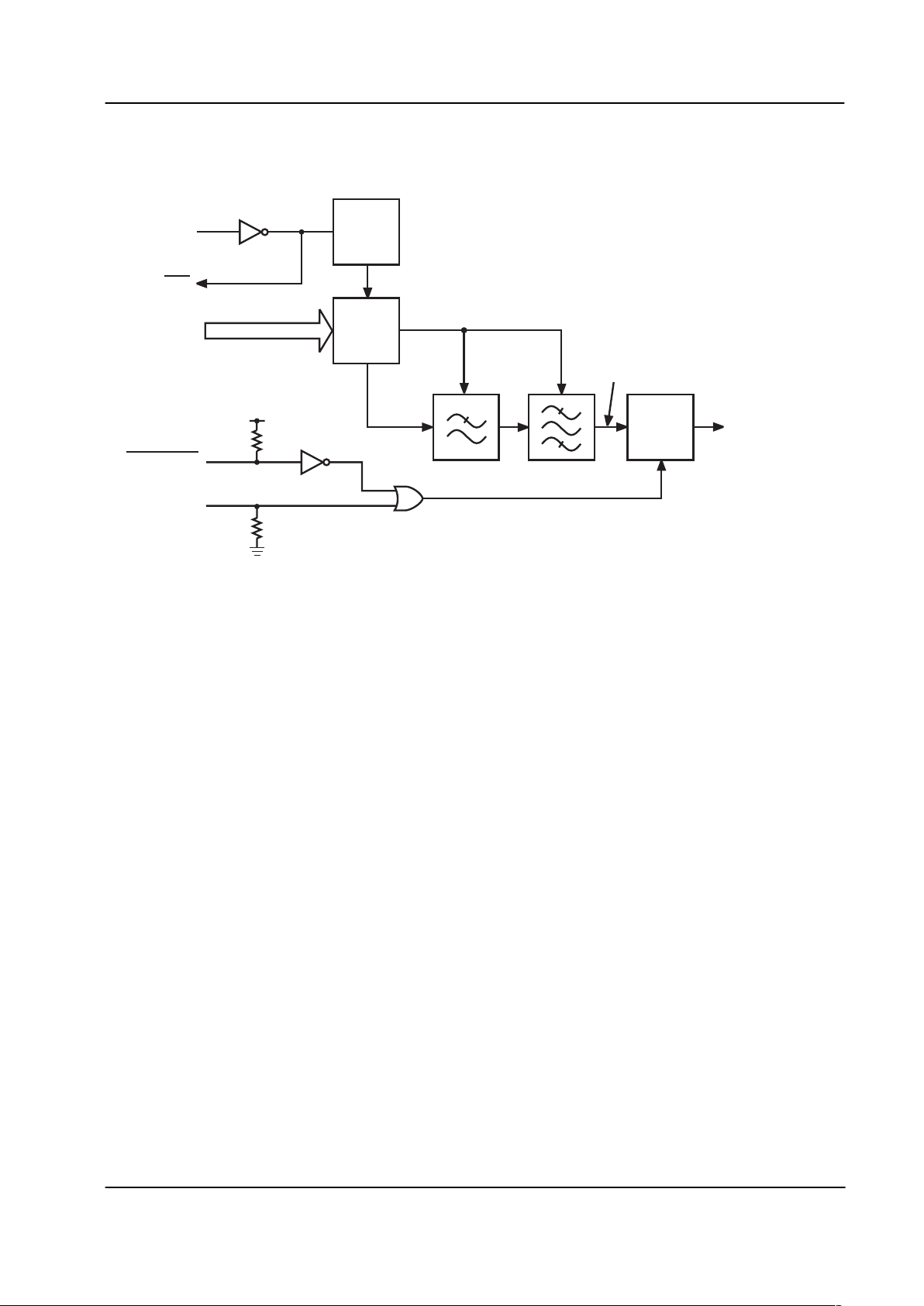
1. Block Diagram
Xtal/Clock
Clock
Generator
D0-D5
Xtal
Binary
Rate
Multiplier
TX Enable
TX Enable
V
DD
Programmed Clocks
TX Tone
Square
Wave
TX Tone
Sinewave
Output
Emitter
Follower
Enable
TX Tone Output
Figure 1: Device Block Diagram
Page 4

CTCSS Encoder 4 MX315A
1998 MXCOM, INC. www.mxcom.com tel: 800 638 5577 336 744 5050 fax: 336 744 5054 Doc. # 20480054.006
4800 Bethania Station Road, Winston-Salem, NC 27105-1201 USA All Trademarks and service marks are held by there respective companies.
2. Signal List
Pins Signal
J,P DW Name Type
Description
1 1 D3 input
2 2 D2 input
3 3 D1 input
4 4 D0 input
5 5 D4 input
6 6 D5 input
D0-D5 are tone select inputs with internal pull-up resistors.
The logic combination at these inputs determines the encoded
CTCSS tone. See Table 1. The input sequence is not latched
and may be changed at any time. A logic “1” will be
programmed if the input is open circuit, allowing the use of
SPST switches.
77 V
SS
power Negative Supply Voltage.
8 8 Xtal/Clock In input
This is the input to the CMOS inverter. It can be used in
conjunction with the Xtal output to form the active element in a
crystal oscillator circuit. Alternatively, a logic level 1MHz
frequency can be injected at this pin. However, the supply
voltage should never be applied without the input clock signal.
99
Xtal Output
output This is the output of the CMOS inverter. When used as a
crystal oscillator, track lengths and loading of this pin should be
minimized.
10 10 Internal Connection Do not use
11 N/C No Connection
12 N/C No Connection
11 13 TX Tone Output output
This is the tone output pin. It includes a low impedance emitter
follower stage for sourcing sinusoidal tone. The tone is
generated about a DC level of approximately V
DD
/2. The pin is
high impedance when not encoding.
12 14
TX Enable Input
input This logic input has an internal pull-up resistor. A logic “0” at
this pin enables the MX315A.
13 15 TX Enable Input input
This logic input has an internal pull-down resistor. A logic “1”
at this pin enables the MX315A.
14 16 V
DD
power Positive Supply Voltage.
Table 1: Signal List
Page 5

CTCSS Encoder 5 MX315A
1998 MXCOM, INC. www.mxcom.com tel: 800 638 5577 336 744 5050 fax: 336 744 5054 Doc. # 20480054.006
4800 Bethania Station Road, Winston-Salem, NC 27105-1201 USA All Trademarks and service marks are held by there respective companies.
3. External Components
MICROPHONE
VOICE BAND
FILTER
SUMMING
AMPLIFIER
TO
MODULATOR
TX TONE OUT
X1
1MHz
1M
33pF
PTT
12
9
8
XTAL/CLOCK
TX ENABLE
XTAL
4
3
215
6
11
D0
D1 D2D3D4
D5
V
SS
MX315AJ
Figure 2: External Components
R1 Note 1 1M
20%
C1 33pF
20%
X1 Note 2, 3 1MHz
0.19%
Table 2: Recommended External Components
Notes:
1. The 1M resistor is used to bias the internal CMOS inverter into its linear mode. A tolerance of ±20%
is acceptable.
2. “X1” is a parallel resonant crystal. A reference frequency of 1MHz ±0.19% is required to maintain a
tone accuracy within 0.5%.
3. For best results, a crystal oscillator design should drive the clock inverter input with signal levels of at
least 40% of V
DD
, peak to peak. Tuning fork crystals generally cannot meet this requirement. To
obtain crystal oscillator design assistance, consult your crystal manufacturer.
Page 6

CTCSS Encoder 6 MX315A
1998 MXCOM, INC. www.mxcom.com tel: 800 638 5577 336 744 5050 fax: 336 744 5054 Doc. # 20480054.006
4800 Bethania Station Road, Winston-Salem, NC 27105-1201 USA All Trademarks and service marks are held by there respective companies.
4. Application
The MX315A is dedicated to Continuous Tone-controlled Squelch Systems (CTCSS) in radio applications.
However, it can be used wherever encoding of low-frequency tones is required, such as intercoms, door-entry
systems and various industrial applications.
The performance of a CTCSS system can be degraded if speech frequencies in the signaling spectrum are
not removed prior to transmission. This can be accomplished by filtering the microphone signals to attenuate
frequencies below 250 Hz. Figure 2 illustrates the addition of TX Tone Output to the filtered microphone
signals prior to modulation. Figure 3 illustrates the TX Tone Output sequence and a typical spectral analysis.
Where two or more circuits are required to use a single oscillator (i.e. repeater applications), the signal at
Xtal
can be used to drive one additional Xtal/Clock input. Any further circuits can be driven from the buffered
Xtal
output of the second device.
The program code can be set on the D0-D5 inputs by hardwired logic levels or SPST switches to V
SS
, as
illustrated in Figure 2 (allowing the internal pull-up resistors to program a logic “1”).
The MX315A provides both a
TX Enable
input and a TX Enable input. Either input can be used to enable the
tone output, with the unused pin left open circuit (internal resistors establish a valid logic level and prevent
damage). Any configuration of PTT switch or TX signal can therefore be interfaced.
TX ENABLE
TX TONE
OUTPUT
RISE-TIME
ENVELOPE
D.C. GROUND D.C. GROUND
RELATIVE HARMONIC
LEVELS (dB)
FREQUENCY
0
10
20
30
40
50
60
70
FUNDAMENT AL
TX TONE SPECTRUM
f02f
0
3f
0
4f05f
0
6f
0
7f08f
0
Figure 3: Tone Encoding Sequence and Spectral Response
4.1 Interfacing and Electromagnetic Capability
The MX315A requires a clock of 1MHz, which is internally converted to logic level square waves.
Consideration should therefore be given to possible interference problems with RF or IF circuitry caused by
1MHz or its harmonics.
A decoupling capacitor can be used to reduce ripple on the power supply. This will reduce the level of
superimposed noise on the supply caused by internal switching transients (particularly at 1MHz and f
0
).
Page 7

CTCSS Encoder 7 MX315A
1998 MXCOM, INC. www.mxcom.com tel: 800 638 5577 336 744 5050 fax: 336 744 5054 Doc. # 20480054.006
4800 Bethania Station Road, Winston-Salem, NC 27105-1201 USA All Trademarks and service marks are held by there respective companies.
4.2 CTCSS Programming
Tone Programming Inputs
Nominal Frequency (Hz) MX315A Freq. (Hz)
fo (%)
D5 D4 D3 D2 D1 D0 Hex
67.0 67.06 +.10 1 1 1 1 1 1 3F
69.3 69.37 +.10 1 1 1 0 0 1 39
71.9 71.84 -.08 0 1 1 1 1 1 1F
74.4 74.33 -.10 1 1 1 1 1 0 3E
77.0 76.99 -.02 0 0 1 1 1 1 0F
79.7 79.65 -.06 1 1 1 1 0 1 3D
82.5 82.50 0.0 0 1 1 1 1 0 1E
85.4 85.34 -0.7 1 1 1 1 0 0 3C
88.5 88.62 +.14 0 0 1 1 1 0 0E
91.5 91.38 -.13 1 1 1 0 1 1 3B
94.8 94.88 +.08 0 1 1 1 0 1 1D
97.4 97.46 +.06 1 1 1 0 1 0 3A
100.0 99.87 -.13 0 0 1 1 0 1 0D
103.5 103.39 -.11 0 1 1 1 0 0 1C
107.2 107.17 -.03 0 0 1 1 0 0 0C
110.9 110.85 -.04 0 1 1 0 1 1 1B
114.8 114.80 0.0 0 0 1 0 1 1 0B
118.8 118.60 -.17 0 1 1 0 1 0 1A
123.0 123.12 +.10 0 0 1 0 1 0 0A
127.3 127.50 +.16 0 1 1 0 0 1 19
131.8 131.67 -.10 0 0 1 0 0 1 09
136.5 136.69 +.14 0 1 1 0 0 0 18
141.3 141.48 +.13 0 0 1 0 0 0 08
146.2 145.96 -.16 0 1 0 1 1 1 17
151.4 151.45 +.03 0 0 0 1 1 1 07
156.7 156.59 -.07 0 1 0 1 1 0 16
162.2 162.10 -.06 0 0 0 1 1 0 06
167.9 168.01 +.07 0 1 0 1 0 1 15
173.8 173.43 -.21 0 0 0 1 0 1 05
179.9 180.21 +.17 0 1 0 1 0 0 14
186.2 186.46 +.14 0 0 0 1 0 0 04
192.8 193.16 +.19 0 1 0 0 1 1 13
203.5 202.88 -.31 0 0 0 0 1 1 03
206.5 206.78 +.14 1 1 1 0 0 0 38
210.7 210.84 +.07 0 1 0 0 1 0 12
218.1 217.96 -.07 0 0 0 0 1 0 02
225.7 225.58 -.05 0 1 0 0 0 1 11
233.6 233.75 +.07 0 0 0 0 0 1 01
241.8 242.54 +.31 0 1 0 0 0 0 10
250.3 250.06 +.10 0 0 0 0 0 0 00
Test 4032 0.0 1 1 0 0 1 1 *33
* - or any invalid address
Table 3: CTCSS Tones
Page 8

CTCSS Encoder 8 MX315A
1998 MXCOM, INC. www.mxcom.com tel: 800 638 5577 336 744 5050 fax: 336 744 5054 Doc. # 20480054.006
4800 Bethania Station Road, Winston-Salem, NC 27105-1201 USA All Trademarks and service marks are held by there respective companies.
5. Performance Specification
5.1 Electrical Performance
5.1.1 Absolute Maximum Ratings
Exceeding these maximum ratings can result in damage to the device.
General Min. Max. Units
Supply Voltage -0.3 7.0 V
J / P /DW Packages
Total Allowable Device Dissipation at T
AMB
= 25°C 800 mW
Derating above 25°C 10 mW/°C above 25°C
Operating Temperature -30 +85 °C
Storage Temperature -55 +125 °C
5.1.2 Operating Limits
Correct operation of the device outside these limits is not implied.
Notes Min. Typ. Max. Units
V
DD
4.5 5.0 5.5 V
Operating Temperature -30 85 °C
Clock Note 1 1 MHz
Operating Limits Note:
1. “X1” is a parallel resonant crystal. A reference frequency of 1 MHz ±0.19% is required to maintain a
tone accuracy within 0.5%.
5.1.3 Operating Characteristics
For the following conditions unless otherwise specified:
V
DD
= 5.0V , T
AMB
= 25°C, Xtal Frequency = 1MHz
Notes Min. Typ. Max Units
Supply Current (operating) 1.5 4.5 mA
Input Impedance 1 500
k
Input Impedance 2 10
M
Logic Input “1” 3.5 V
Logic Input “0” 1.5 V
TX Output EMF 3 550 775 mV
RMS
TX Risetime 1 ms
TX Tone Output Load Current 5 mA
TX Distortion 3 2 5 %
Variation in Output Level Between Tones 3 0.1 dB
Operating Characteristics Notes:
1. Refers to D0, D1, D2, D3, D4, D5, TX Enable and
TX Enable
inputs
2. Refers to Xtal/Clock input
3. Any program tone and R
L
= 600, CL = 15pF. THD measurements are taken in the 0-6 kHz
bandwidth.
Page 9

CTCSS Encoder 9 MX315A
1998 MXCOM, INC. www.mxcom.com tel: 800 638 5577 336 744 5050 fax: 336 744 5054 Doc. # 20480054.006
4800 Bethania Station Road, Winston-Salem, NC 27105-1201 USA All Trademarks and service marks are held by there respective companies.
5.2 Packaging
PIN 1
A
B
ALTERNATIVE
PIN
LOCATION
MARKING
X
P
J
Y
C
K
H
E
L
T
W
Z
NOTE: All dimensions in inches (mm.)
Angles are in degrees
PackageTolerances
A
B
C
E
H
TYP.
MAX.MIN.
DIM.
J
P
X
W
T
Y
K
L
0.105 (2.67)0.093 (2.36)
0.419 (10.64)
45°
7°
0° 10°
0.050 (1.27)
0.041 (1.04)
0.413 (10.49)
0.299 (7.59)
0.050 (1.27)
0.016 (0.41)
0.390 (9.90)
0.020 (0.51)0.003 (0.08)
0.009 (0.23) 0.0125 (0.32)
0.013 (0.33) 0.020 (0.51)
0.395 (10.03)
0.286 (7.26)
Z
5°
5°
Figure 4: 16-pin SOIC Mechanical Outline: Order as part no. MX315ADW
PackageTolerances
B
A
PIN 1
E
Y
E1
T
NOTE: All dimensions in inches (mm.)
Angles are in degrees
A
B
C
E
E1
H
TYP. MAX.MIN.
DIM.
J
J1
P
T
Y
K
L
0.200 (5.06)
0.260 (6.60)
0.390 (9.91)
7°
0.150 (3.81)
0.810 (20.57)
0.135 (3.43)
0.100 (2.54)
0.121 (3.07)
0.300 (7.62)
0.290 (7.37) 0.325 (8.26)
0.015 (0.38) 0.070 (1.77)
0.015 (0.38) 0.023 (0.58)
0.040 (1.01) 0.065 (1.65)
0.056 (1.42) 0.064 (1.63)
0.740 (18.80)
0.240 (6.10)
0.008 (0.20) 0.015 (0.38)
K
H
J1
J
C
P
L
Figure 5: 14-pin PDIP Mechanical Outline: Order as part no. MX315AP
Page 10

CTCSS Encoder 10 MX315A
1998 MXCOM, INC. www.mxcom.com tel: 800 638 5577 336 744 5050 fax: 336 744 5054 Doc. # 20480054.006
4800 Bethania Station Road, Winston-Salem, NC 27105-1201 USA All Trademarks and service marks are held by there respective companies.
NOTE: All dimensions in inches (mm.)
Angles are in degrees
PackageTolerances
A
B
E
E1
F
H
TYP. MAX.MIN.
DIM.
J
P
T
K1
K
L
0.288 (7.32)
0.420 (10.67)
0.200 (5.08)
0.766 (19.46)
0.100 (2.54)
0.115 (2.92)
0.360 (9.14)
0.305 (7.75) 0.315 (8.00)
0.600 (15.24)
0.015 (0.38)
0.018 (0.46)
0.053 (1.35)
0.075 (1.91)
0.080 (2.03)
0.080 (2.03)
0.754 (19.15)
0.240 (6.10)
0.010 (0.254)
C
0.165 (4.19) 0.230 (5.84)
J1
0.060 (1.52)
E1
T
E
B
A
PIN 1
H
K
F
J
K1
P
L
C
J1
Figure 6: 14-pin CDIP Mechanical Outline: Order as part no. MX315AJ
 Loading...