

Datasheet MX29LV004BQC-55R, MX29LV004BQC-70, MX29LV004BQC-90, MX29LV004BQI-70, MX29LV004BQI-90 Datasheet (MXIC)
...Page 1

FEA TURES
PRELIMINARY
MX29LV004T/B
4M-BIT [512K x 8] CMOS SINGLE VOLTAGE
3V ONLY FLASH MEMORY
• Extended single - supply voltage range 2.7V to 3.6V
• 524,288 x 8
• Single power supply operation
- 3.0V only operation for read, erase and program
operation
• Fast access time: 55R/70/90ns
• Low power consumption
- 20mA maximum active current
- 0.2uA typical standby current
• Command register architecture
- Byte Programming (9us typical)
- Sector Erase (Sector structure 16K-Byte x 1,
8K-Byte x 2, 32K-Byte x1, and 64K-Byte x7)
• Auto Erase (chip & sector) and Auto Program
- Automatically erase any combination of sectors with
Erase Suspend capability.
- Automatically program and verify data at specified
address
• Erase suspend/Erase Resume
- Suspends sector erase operation to read data from,
or program data to, any sector that is not being erased,
then resumes the erase.
• Status Reply
- Data polling & Toggle bit for detection of program and
erase operation completion.
• Ready/Busy pin (RY/BY)
- Provides a hardware method of detecting program or
erase operation completion.
• Sector protection
- Hardware method to disable any combination of
sectors from program or erase operations
- Tempoary sector unprotect allows code changes in
previously locked sectors.
• 100,000 minimum erase/program cycles
• Latch-up protected to 100mA from -1V to VCC+1V
• Boot Sector Architecture
- T = Top Boot Sector
- B = Bottom Boot Sector
• Low VCC write inhibit is equal to or less than 2.3V
• Package type:
- 40-pin TSOP
- 32-pin PLCC
• Compatibility with JEDEC standard
- Pinout and software compatible with single-power
supply Flash
GENERAL DESCRIPTION
The MX29LV004T/B is a 4-mega bit Flash memory organized as 512K bytes of 8 bits. MXIC's Flash memories offer the most cost-effective and reliable read/write
non-volatile random access memory . The MX29L V004T/
B is packaged in 40-pin TSOP and 32-pin PLCC. It is
designed to be reprogrammed and erased in system or
in standard EPROM programmers.
The standard MX29L V004T/B off ers access time as fast
as 55ns, allowing operation of high-speed microprocessors without wait states. To eliminate bus contention,
the MX29L V004T/B has separate chip enab le (CE) and
output enable (OE) controls.
MXIC's Flash memories augment EPROM functionality
with in-circuit electrical erasure and programming. The
MX29LV004T/B uses a command register to manage
this functionality . The command register allo ws for 100%
P/N:PM0732 REV. 1.1, SEP. 19, 2001
TTL level control inputs and fixed power supply levels
during erase and programming, while maintaining maximum EPROM compatibility.
MXIC Flash technology reliably stores memory contents
even after 100,000 erase and prog ram cycles. The MXIC
cell is designed to optimize the erase and programming
mechanisms. In addition, the combination of advanced
tunnel oxide processing and low internal electric fields
for erase and program operations produces reliable cycling. The MX29LV004T/B uses a 2.7V~3.6V VCC supply to perform the High Reliability Erase and auto Program/Erase algorithms.
The highest degree of latch-up protection is achieved
with MXIC's proprietary non-epi process. Latch-up protection is proved for stresses up to 100 milliamps on
address and data pin from -1V to VCC + 1V.
1
Page 2

PIN CONFIGURATIONS
40 TSOP (Standard Type) (10mm x 20mm)
NC
1
2
3
4
5
6
7
A9
8
A8
9
10
11
12
13
14
A7
15
A6
16
A5
17
A4
18
A3
19
A2
20
A1
A16
A15
A14
A13
A12
A11
WE
RESET
RY/BY
A18
MX29LV004T/B
MX29LV004T/B
40
A17
39
GND
38
NC
37
NC
36
A10
35
Q7
34
Q6
33
Q5
32
Q4
31
VCC
30
VCC
29
NC
28
Q3
27
Q2
26
Q1
25
Q0
24
OE
23
VSS
22
CE
21
A0
32 PLCC
A12
A15
4
5
A7
A6
A5
A4
MX29LV004T/B
9
A3
A2
A1
A0
13
Q0
14 17 20
Q1
Q2
A16
1
GND
A18
VCCWEA17
32
Q3Q4Q5
PIN DESCRIPTION
SYMBOL PIN NAME
30
29
A14
A13
A8
A9
25
A11
OE
A10
CE
21
Q7
Q6
A0~A18 Address Input
Q0~Q7 Data Input/Output
CE Chip Enable Input
WE Write Enable Input
RESET Hardware Reset Pin/Sector Protect Unlock
(for 40-TSOP)
OE Output Enable Input
RY/BY Ready/Busy Output (for 40-TSOP)
VCC Power Supply Pin (2.7V~3.6V)
GND Ground Pin
P/N:PM0732
REV. 1.1, SEP. 19, 2001
2
Page 3

MX29LV004T/B
BLOCK STRUCTURE
Table 1: MX29LV004T SECTOR ARCHITECTURE
Sector Sector Size Address range Sector Address
Byte Mode Byte Mode (x8) A18 A1 7 A1 6 A1 5 A1 4 A 13
SA0 64Kbytes 00000-0FFFF 0 0 0 X X X
SA1 64Kbytes 10000-1FFFF 0 0 1 X X X
SA2 64Kbytes 20000-2FFFF 0 1 0 X X X
SA3 64Kbytes 30000-3FFFF 0 1 1 X X X
SA4 64Kbytes 40000-4FFFF 1 0 0 X X X
SA5 64Kbytes 50000-5FFFF 1 0 1 X X X
SA6 64Kbytes 60000-6FFFF 1 1 0 X X X
SA7 32Kbytes 70000-77FFF 1 1 1 0 X X
SA8 8Kbytes 78000-79FFF 1 1 1 1 0 0
SA9 8Kbytes 7A000-7BFFF 1 1 1 1 0 1
SA10 16Kbytes 7C000-7FFFF 1 1 1 1 1 X
Table 2: MX29LV004B SECTOR ARCHITECTURE
Sector Sector Size Address range Sector Address
Byte Mode Byte Mode (x8) A18 A1 7 A 1 6 A 1 5 A1 4 A 1 3
SA0 16Kbytes 00000-03FFF 0 0 0 0 0 X
SA1 8Kbytes 04000-05FFF 0 0 0 0 1 0
SA2 8Kbytes 06000-07FFF 0 0 0 0 1 1
SA3 32Kbytes 08000-0FFFF 0 0 0 1 X X
SA4 64Kbytes 10000-1FFFF 0 0 1 X X X
SA5 64Kbytes 20000-2FFFF 0 1 0 X X X
SA6 64Kbytes 30000-3FFFF 0 1 1 X X X
SA7 64Kbytes 40000-4FFFF 1 0 0 X X X
SA8 64Kbytes 50000-5FFFF 1 0 1 X X X
SA9 64Kbytes 60000-6FFFF 1 1 0 X X X
SA10 64Kbytes 70000-7FFFF 1 1 1 X X X
P/N:PM0732
REV. 1.1, SEP. 19, 2001
3
Page 4

BLOCK DIAGRAM
MX29LV004T/B
CE
OE
WE
RESET
A0-A18
(for 40-TSOP)
CONTROL
INPUT
LOGIC
ADDRESS
LATCH
AND
BUFFER
PROGRAM/ERASE
HIGH VOLTAGE
X-DECODER
MX29L V004T/B
FLASH
ARRA Y
Y-DECODER
Y-PASS GATE
SENSE
AMPLIFIER
PGM
DATA
ARRAY
SOURCE
HV
HV
WRITE
STATE
MACHINE
(WSM)
STATE
REGISTER
COMMAND
DATA
DECODER
COMMAND
DATA LATCH
P/N:PM0732
Q0-Q7
PROGRAM
DATA LATCH
I/O BUFFER
REV. 1.1, SEP. 19, 2001
4
Page 5

MX29LV004T/B
AUTOMATIC PROGRAMMING
The MX29L V004T/B is byte programmab le using the Automatic Programming algorithm. The Automatic Programming algorithm makes the external system do not
need to have time out sequence nor to verify the data
programmed. The typical chip programming time at room
temperature of the MX29LV004T/B is less than 10 seconds.
AUTOMATIC CHIP ERASE
The entire chip is bulk erased using 10 ms erase pulses
according to MXIC's Automatic Chip Erase algorithm.
T ypical erasure at room temper ature is accomplished in
less than 25 second. The Automatic Erase algorithm
automatically programs the entire array prior to electrical erase. The timing and v erification of electrical erase
are controlled internally within the device.
AUTOMATIC SECTOR ERASE
The MX29L V004T/B is sector(s) erasab le using MXIC's
Auto Sector Erase algorithm. The Automatic Sector
Erase algorithm automatically programs the specified
sector(s) prior to electrical erase. The timing and verification of electrical erase are controlled internally within
the device. An erase operation can erase one sector,
multiple sectors, or the entire device.
AUTOMATIC PROGRAMMING ALGORITHM
MXIC's Automatic Programming algorithm requires the
user to only write program set-up commands (including
2 unlock write cycle and A0H) and a program command
(program data and address). The device automatically
times the programming pulse width, provides the program verification, and counts the number of sequences.
The device provides an unlock bypass mode with faster
programming. Only two write cycles are needed to program a byte, instead of f our. A status bit similar to D AT A
polling and a status bit toggling between consecutive
read cycles, provide feedback to the user as to the status of the programming operation. Refer to write operation status, table7, for more information on these status
bits.
AUTOMATIC ERASE ALGORITHM
MXIC's Automatic Erase algorithm requires the user to
write commands to the command register using standard microprocessor write timings. The device will automatically pre-program and verify the entire array. Then
the device automatically times the erase pulse width,
provides the erase verification, and counts the number
of sequences. A status bit toggling between consecutive read cycles provides feedback to the user as to the
status of the erasing operation.
Register contents serve as inputs to an internal statemachine which controls the erase and programming circuitry . During write cycles, the command register internally latches address and data needed for the programming and erase operations. During a system write cycle,
addresses are latched on the falling edge, and data are
latched on the rising edge of WE or CE, whichev er happens first.
MXIC's Flash technology combines years of EPROM
experience to produce the highest lev els of quality, reliability , and cost effectiv eness. The MX29LV004T/B electrically erases all bits simultaneously using FowlerNordheim tunneling. The bytes are prog rammed by using the EPROM programming mechanism of hot electron injection.
During a program cycle, the state-machine will control
the program sequences and command register will not
respond to any command set. During a Sector Erase
cycle, the command register will only respond to Erase
Suspend command. After Erase Suspend is completed,
the device stays in read mode. After the state machine
has completed its task, it will allow the command register to respond to its full command set.
AUTOMATIC SELECT
The automatic select mode provides manufacturer and
device identification, and sector protection verification,
through identifier codes output on Q7~Q0. This mode is
mainly adapted for programming equipment on the device to be programmed with its programming algorithm.
When programming by high voltage method, automatic
select mode requires VID (11.5V to 12.5V) on address
pin A9 and other address pin A6, A1 as referring to Table
3. In addition, to access the automatic select codes insystem, the host can issue the automatic select com-
P/N:PM0732
REV. 1.1, SEP. 19, 2001
5
Page 6

MX29LV004T/B
mand through the command register without requiring
VID , as sho wn in table4.
T o v erify whether or not sector being protected, the sector address must appear on the appropriate highest order address bit (see Table 1 and Table 2). The rest of
address bits, as shown in table3, are don't care. Once
all necessary bits have been set as required, the programming equipment may read the corresponding identifier code on Q7~Q0.
T ABLE 3. MX29LV004T/B AUTOSELECT MODE OPERA TION
A18 A12 A9 A8 A6 A5 A1 A0
Description CE OE WE RESET | | | | Q15~Q0
(note) A13 A10 A7 A2
Read Silicon ID L L H H X X VID X L X L L C2 H
Manfacturer Code
Read Silicon ID L L H H X X VID X L X L H B5H
(Top Boot Block)
Device ID L L H H X X VID X L X L H B6H
(Bottom Boot Block)
Sector Protection L L H H SA X VID X L X H L (protected)
Verification 00H
(unprotected)
01H
NO T E: SA=Sector Address, X=Don't Care, L=Logic Lo w , H=Logic High.
RESET pin for 40-TSOP only.
P/N:PM0732
6
REV. 1.1, SEP. 19, 2001
Page 7

MX29LV004T/B
T ABLE 4. MX29LV004T/B COMMAND DEFINITIONS
First Bus Second Bus Third Bus Fourth Bus Fifth Bus Sixth Bus
Command Bus Cycle Cycle Cycle Cycle Cycle Cycle
Cycle Addr Data Addr Data Addr Data Addr Data Addr Data Addr Data
Reset 1 XXXH F0H
Read 1 RA RD
Read Silicon ID 4 555H AAH 2AAH 5 5H 555H 90H ADI DDI
Sector Protect 4 555H AAH 2AAH 5 5 H 555H 90H (SA) 00H
Verify x02H 01 H
Porgram 4 555H AAH 2AAH 55H 555H A0H PA PD
Chip Erase 6 555H AAH 2AAH 5 5H 555H 80H 555H AAH 2AAH 55H 555H 10H
Sector Erase 6 555H AAH 2AAH 5 5H 555H 80H 555H AAH 2AAH 5 5H SA 30 H
Sector Erase Suspend 1 XXXH B0H
Sector Erase Resume 1 XXXH 3 0H
Note:
1 . ADI = Address of Device identifier; A1=0, A0 = 0 for manufacturer code,A1=0, A0 = 1 for device code. A2-A17=do
not care.
(Refer to table 3)
DDI = Data of Device identifier : C2H f or man uf acture code, B5H/B6H (Top/Bottom) for device code.
X = X can be VIL or VIH
RA=Address of memory location to be read.
RD=Data to be read at location RA.
2. P A = Address of memory location to be programmed.
PD = Data to be programmed at location PA.
SA = Address of the sector to be erased.
3. The system should generate the following address patterns: 555H or 2AAH to Address A11~A0.
Address bit A12~A18=X=Don't care for all address commands except f or Progr am Address (PA) and Sector
Address (SA). Write Sequence may be initiated with A12~A18 in either state .
4. For Sector Protect Verify operation:If read out data is 01H, it means the sector has been protected. If read out
data is 00H, it means the sector is still not being protected.
P/N:PM0732
REV. 1.1, SEP. 19, 2001
7
Page 8

COMMAND DEFINITIONS
MX29LV004T/B
Device operations are selected by writing specific address and data sequences into the command register.
Writing incorrect address and data values or writing them
sequences. Note that the Erase Suspend (B0H) and
Erase Resume (30H) commands are valid only while the
Sector Erase operation is in progress.
in the improper sequence will reset the device to the
read mode. Table 4 defines the valid register command
T ABLE 5. MX29LV004T/B BUS OPERA TION
ADDRESS Q8~Q15
DESCRIPTION CE OE WE RESET A18 A12 A9 A8 A6 A5 A 1 A0 Q0~Q7 BYTE BYTE
(8) A 13 A10 A7 A2 =VIH =VIL
Read L L H H AIN Dout Dout Q8~Q14=High Z
Q15=A-1
Write L H L H AIN DIN(3) DIN Q8~Q14=High Z
Q15=A-1
Reset X X X L X High Z High Z High Z
Temproary sector unlock X X X VID AIN DI N D IN High Z
Output Disable L H H H X High Z High Z High Z
Standby Vcc ± X X Vcc± X High Z High Z High Z
0.3V 0.3V
Sector Protect L H L VID SA X X X L X H L D IN X X
Chip Unprotect L H L VID X X X X H X H L DI N X X
Sector Protection Verify L L H H SA X VID X L X H L CODE(5) X X
NOTES:
1. Manufacturer and device codes may also be accessed via a command register write sequence. Refer to Table 4.
2. VID is the Silicon-ID-Read high voltage, 11.5V to 12.5V.
3. Refer to Table 4 for valid Data-In during a write operation.
4. X can be VIL or VIH.
5. Code=00H means unprotected.
Code=01H means protected.
6. A18~A13=Sector address for sector protect.
7. The sector protect and chip unprotect functions may also be implemented via programming equipment.
8. RESET pin for 40-TSOP package type only.
P/N:PM0732
8
REV. 1.1, SEP. 19, 2001
Page 9

MX29LV004T/B
REQUIREMENTS FOR READING ARRAY
DATA
To read array data from the outputs, the system must
drive the CE and OE pins to VIL. CE is the pow er control
and selects the device. OE is the output control and gates
array data to the output pins. WE should remain at VIH.
The internal state machine is set for reading array data
upon device power-up, or after a hardware reset. This
ensures that no spurious alteration of the memory contect
occurs during the power transition. No command is
necessary in this mode to obtain array data. Standard
microprocessor read cycles that assert valid address on
the device address inputs produce valid data on the device
data outputs. The device remains enab led for read access
until the command register contents are altered.
WRITE COMMANDS/COMMAND
SEQUENCES
T o program data to the de vice or erase sectors of memory
, the sysytem must drive WE and CE to VIL, and OE to
VIH.
Refer to the Autoselect Mode and Autoselect Command
Sequence section for more information.
ICC2 in the DC Characteristics table represents the
active current specification for the write mode. The "A C
Characteristics" section contains timing specification
table and timing diagrams for write operations.
STANDBY MODE
When using both pins of CE and RESET, the device
enter CMOS Standby with both pins held at Vcc ± 0.3V.
The RESET pin is provided only for 40-pin TSOP package type. If CE and RESET are held at VIH, but not
within the range of V CC ± 0.3V , the de vice will still be in
the standby mode, but the standb y current will be larger.
During Auto Algorithm operation, Vcc active current
(Icc2) is required even CE = "H" until the operation is
complated. The device can be read with standard access time (tCE) from either of these standby modes,
before it is ready to read data.
OUTPUT DISABLE
The device features an Unlock Bypass mode to facilitate
faster programming. Once the device enters the Unlock
Bypass mode, only two write cycles are required to
program a byte, instead of four. The "byte Program
Command Sequence" section has details on
programming data to the device using both standard and
Unlock Bypass command sequences.
An erase operation can erase one sector , multiple sectors
, or the entire device. Table indicates the address space
that each sector occupies. A "sector address" consists
of the address bits required to uniquely select a sector.
The "Writing specific address and data commands or
sequences into the command register initiates device
operations. Table 1 defines the valid register command
sequences. Writing incorrect address and data values or
writing them in the improper sequence resets the device
to reading array data."section has details on erasing a
sector or the entire chip, or suspending/resuming the erase
operation.
After the system writes the autoselect command
sequence, the device enters the autoselect mode. The
system can then read autoselect codes from the internal
reqister (which is separate from the memory array) on
Q7-Q0. Standard read cycle timings apply in this mode.
With the OE input at a logic high level (VIH), output from
the devices are disabled. This will cause the output pins
to be in a high impedance state.
RESET OPERATION (for 40-TSOP package type)
The RESET pin provides a hardware method of resetting
the device to reading arra y data. When the RESET pin is
driven low for at least a period of tRP, the device
immediately terminates any operation in progress,
tristates all output pins, and ignores all read/write
commands for the duration of the RESET pluse. The
device also resets the internal state machine to reading
array data. The operation that was interrupted should be
reinitated once the device is ready to accept another
command sequence, to ensure data integrity
Current is reduced for the duration of the RESET pulse.
When RESET is held at VSS±0.3V, the device draws
CMOS standby current (ICC4). If RESET is held at VIL
but not within VSS±0.3V, the standby current will be
greater.
The RESET pin may be tied to system reset circuitry . A
system reset would that also reset the Flash memory ,
P/N:PM0732
REV. 1.1, SEP. 19, 2001
9
Page 10

MX29LV004T/B
enabling the system to read the boot-up firm-ware from
the Flash memory .
If RESET is asserted during a program or erase
operation, the R Y/BY pin remains a "0" (b usy) until the
internal reset operation is complete, which requires a
time of tREADY (during Embedded Algorithms). The
sysytem can thus monitor RY/BY to determine whether
the reset operation is complete. If RESET is asserted
when a program or erase operation is commpleted within
a time of tREADY (not during Embedded Algorithms).
The system can read data tRH after the RESET pin
returns to VIH.
Refer to the AC Characteristics tables for RESET
parameters and to Figure 24 for the timing diagram.
READ/RESET COMMAND
The read or reset operation is initiated by writing the
read/reset command sequence into the command register. Microprocessor read cycles retrieve array data.
The device remains enabled for reads until the command
register contents are altered.
If program-fail or erase-fail happen, the write of F0H will
reset the device to abort the operation. A valid command must then be written to place the device in the
desired state.
SET-UP AUTOMATIC CHIP/SECTOR ERASE
COMMANDS
Chip erase is a six-bus cycle operation. There are two
"unlock" write cycles. These are followed b y writing the
"set-up" command 80H. Two more "unlock" write cycles are then followed by the chip erase command 10H
or sector erase command 30H.
The Automatic Chip Erase does not require the device
to be entirely pre-programmed prior to executing the Automatic Chip Erase. Upon executing the Automatic Chip
Erase, the device will automatically program and verify
the entire memory for an all-zero data pattern. When the
device is automatically verified to contain an all-zero
pattern, a self-timed chip erase and verify begin. The
erase and verify operations are completed when the data
on Q7 is "1" at which time the device returns to the
Read mode. The system is not required to pro vide any
control or timing during these operations.
When using the Automatic Chip Erase algorithm, note
that the erase automatically terminates when adequate
erase margin has been achieved for the memory array(no
erase verification command is required).
If the Erase operation was unsuccessful, the data on
Q5 is "1"(see Table 7), indicating the erase operation
exceed internal timing limit.
SILICON-ID READ COMMAND
Flash memories are intended for use in applications where
the local CPU alters memory contents. As such, manufacturer and device codes must be accessible while the
device resides in the target system. PROM programmers typically access signature codes by raising A9 to
a high voltage(VID). Howev er, m ultiplexing high voltage
onto address lines is not generally desired system design practice.
The MX29L V004T/B contains a Silicon-ID-Read operation to supple traditional PROM programming methodology . The oper ation is initiated by writing the read silicon
ID command sequence into the command register. F ollowing the command write, a read cycle with A1=VIL,
A0=VIL retrieves the manufacturer code of C2H. A read
cycle with A1=VIL, A0=VIH returns the device code of
B5H for MX29LV004T , B6H for MX29LV004B.
P/N:PM0732
The automatic erase begins on the rising edge of the
last WE or CE pulse, whichever happens first in the
command sequence and terminates when the data on
Q7 is "1" and the data on Q6 stops toggling for two consecutive read cycles, at which time the device returns
to the Read mode.
REV. 1.1, SEP. 19, 2001
10
Page 11

MX29LV004T/B
T ABLE 6. EXP ANDED SILICON ID CODE
Pins A0 A1 Q7 Q6 Q5 Q4 Q3 Q2 Q1 Q0 Code(Hex)
Manufacture code VIL VIL 1 1 0 0 0010C2H
Device code VIH VIL 1 0 1 1 100122B9H
for MX29LV004T VIH VIL 1 0 1 1 1001B5H
Device code VIH VIL 1 0 1 1 101022BAH
for MX29LV004B VIH VIL 1 0 1 1 1010B6H
Sector Protection X VIH 0 0 0 0 000101H (Protected)
V erification X VIH 0 0 0 0 000000H (Unprotected)
READING ARRAY DATA
The device is automatically set to reading array data
after device power-up. No commands are required to
retrieve data. The device is also ready to read arra y data
after completing an Automatic Program or Automatic
Erase algorithm.
After the device accepts an Erase Suspend command,
the device enters the Erase Suspend mode. The system can read array data using the standard read timings, except that if it reads at an address within erasesuspended sectors, the device outputs status data. After
completing a programming operation in the Erase
Suspend mode, the system may once again read array
data with the same exception. See rase Suspend/Erase
Resume Commands” for more infor-mation on this mode.
The system
able the device for reading array data if Q5 goes high, or
while in the autoselect mode. See the "Reset Command"
section, next.
must issue the reset command to re-en-
RESET COMMAND
Writing the reset command to the device resets the
device to reading array data. Address bits are don't care
for this command.
The reset command may be written between the sequence cycles in an erase command sequence before
erasing begins. This resets the device to reading array
data. Once erasure begins, however, the device ignores
reset commands until the operation is complete.
The reset command may be written between the sequence cycles in a program command sequence be-fore
programming begins. This resets the device to reading
array data (also applies to programming in Erase
Suspend mode). Once prog ramming begins ,how ever, the
device ignores reset commands until the operation is
complete.
The reset command may be written between the sequence cycles in an SILICON ID READ command
sequence. Once in the SILICON ID READ mode, the
reset command
data (also applies to SILICON ID READ during Erase
Suspend).
must be written to return to reading array
P/N:PM0732
If Q5 goes high during a program or erase operation,
writing the reset command returns the device to reading
array data (also applies during Erase Suspend).
REV. 1.1, SEP. 19, 2001
11
Page 12

SECTOR ERASE COMMANDS
MX29LV004T/B
The Automatic Sector Erase does not require the device to be entirely pre-programmed prior to executing
the Automatic Sector Erase Set-up command and Automatic Sector Erase command. Upon executing the
Automatic Sector Erase command, the device will automatically program and verify the sector(s) memory for
an all-zero data pattern. The system is not required to
provide any control or timing during these operations.
When the sector(s) is automatically verified to contain
an all-zero pattern, a self-timed sector erase and verify
begin. The erase and verify operations are complete
when the data on Q7 is "1" and the data on Q6 stops
toggling for two consecutive read cycles, at which time
the device returns to the Read mode. The system is not
required to provide any control or timing during these
operations.
When using the Automatic sector Erase algorithm, note
that the erase automatically terminates when adequate
erase margin has been achieved for the memory array
T able 7. Write Operation Status
(no erase verification command is required). Sector
erase is a six-bus cycle operation. There are two "unlock" write cycles. These are f ollowed by writing the setup command 80H. Two more "unlock" write cycles are
then followed by the sector erase command 30H. The
sector address is latched on the falling edge of WE or
CE, whichever happens later , while the command(data)
is latched on the rising edge of WE or CE, whichever
happens first. Sector addresses selected are loaded
into internal register on the sixth falling edge of WE or
CE, whichever happens later. Each successive sector
load cycle started by the falling edge of WE or CE,
whichever happens later must begin within 50us from
the rising edge of the preceding WE or CE, whichever
happens first. Otherwise, the loading period ends and
internal auto sector erase cycle starts. (Monitor Q3 to
determine if the sector erase timer window is still open,
see section Q3, Sector Erase Timer .) Any command other
than Sector Erase(30H) or Erase Suspend(B0H) during
the time-out period resets the device to read mode.
Status Q7 Q6 Q5 Q3 Q2 RY/BY
(Note1) (Note2)
Byte Program in Auto Program Algorithm Q7 Toggle 0 N/A N o 0
Auto Erase Algorithm 0 Toggle 0 1 Toggle 0
Erase Suspend Read 1 No 0 N/A Toggle 1
(Erase Suspended Sector) Toggle
In Progress
Erase Suspended Mode Erase Suspend Read Data Data Data Data Data 1
(Non-Erase Suspended Sector)
Erase Suspend Program Q7 Toggle 0 N/A N/A 0
Byte Program in Auto Program Algorithm Q7 Toggle 1 N/A N o 0
Exceeded
Time Limits Auto Erase Algorithm 0 Toggle 1 1 Toggle 0
Erase Suspend Program Q7 Toggle 1 N/A N/A 0
Toggle
Toggle
Note:
1. Q7 and Q2 require a valid address when reading status information. Refer to the appropriate subsection for further
details.
2. Q5 switches to '1' when an Auto Program or Auto Erase operation has exceeded the maximum timing limits.
See "Q5:Exceeded Timing Limits " for more information.
P/N:PM0732
REV. 1.1, SEP. 19, 2001
12
Page 13

MX29LV004T/B
ERASE SUSPEND
This command only has meaning while the state machine is executing Automatic Sector Erase operation,
and therefore will only be responded during Automatic
Sector Erase operation. When the Erase Suspend command is written during a sector erase operation, the device requires a maximum of 20us to suspend the erase
operations. However , When the Erase Suspend command
is written during the sector erase time-out, the device
immediately terminates the time-out period and suspends
the erase operation. After this command has been executed, the command register will initiate erase suspend
mode. The state machine will return to read mode automatically after suspend is ready . At this time, state machine only allows the command register to respond to
the Read Memory Array, Erase Resume and program
commands.
The system can determine the status of the program
operation using the Q7 or Q6 status bits, just as in the
standard program operation. After an erase-suspend program operation is complete, the system can once again
read array data within non-suspended sectors.
The device provides Q2, Q3, Q5, Q6, Q7, and R Y/BY to
determine the status of a write operation. If the program
operation was unsuccessful, the data on Q5 is "1"(see
T ab le 7), indicating the program operation exceed internal timing limit. The automatic programming operation is
completed when the data read on Q6 stops toggling for
two consecutive read cycles and the data on Q7 and Q6
are equivalent to data written to these two bits, at which
time the device returns to the Read mode(no program
verify command is required).
BYTE PROGRAM COMMAND SEQUENCE
The device programs one byte of data for each program
operation. The command sequence requires four bus
cycles, and is initiated by writing two unlock write cycles,
followed by the program set-up command. The program
address and data are written next, which in turn initiate
the Embedded Program algorithm. The system is
required to provide further controls or timings. The device
automatically generates the program pulses and verifies
the programmed cell margin. Table 1 shows the address
and data requirements for the byte program command
sequence.
not
ERASE RESUME
This command will cause the command register to clear
the suspend state and return back to Sector Erase mode
but only if an Erase Suspend command was previously
issued. Erase Resume will not have any effect in all
other conditions. Another Erase Suspend command can
be written after the chip has resumed erasing.
AUTOMATIC PROGRAM COMMANDS
T o initiate Automatic Progr am mode, A three-cycle command sequence is required. There are two "unlock" write
cycles. These are f ollowed by writing the Automatic Program command A0H.
Once the Automatic Program command is initiated, the
next WE pulse causes a tr ansition to an active programming operation. Addresses are latched on the falling
edge, and data are internally latched on the rising edge
of the WE or CE, whichever happens first. The rising
edge of WE or CE, whiche ver happens first, also begins
the programming operation. The system is not required
to provide further controls or timings. The device will
automatically provide an adequate internally generated
program pulse and verify margin.
When the Embedded Program algorithm is complete,
the device then returns to reading array data and
addresses are no longer latched. The system can
determine the status of the program operation by using
Q7, Q6, or RY/BY. See "Write Operation Status" for
information on these status bits.
Any commands written to the device during the Embedded Program Algorithm are ignored. Note that a
hardware reset immediately terminates the programming
operat ion. The Byte Prog ram command sequence should
be reinitiated once the device has reset to reading array
data, to ensure data integrity.
Programming is allowed in any sequence and across
sector boundaries. A bit cannot be programmed from a
"0" back to a "1". Attempting to do so may halt the
operation and set Q5 to "1" ,” or cause the Data Polling
algorithm to indicate the operation was successful.
However, a succeeding read will show that the data is
still "0". Only erase operations can convert a "0" to a
"1".
WRITE OPERSTION STATUS
The device provides several bits to determine the status of a write operation: Q2, Q3, Q5, Q6, Q7, and RY/
P/N:PM0732
REV. 1.1, SEP. 19, 2001
13
Page 14

MX29LV004T/B
BY. Table 10 and the following subsections describe the
functions of these bits. Q7, R Y/BY, and DQ6 each offer
a method for determining whether a program or erase
operation is complete or in progress. These three bits
are discussed first. Please note that RY/BY pin is provided for 40-pin TSOP pac kage type only.
Q7: Data Polling
The Data Polling bit, Q7, indicates to the host sys-tem
whether an Automatic Algorithm is in progress or completed, or whether the device is in Erase Suspend. Data
Polling is v alid after the rising edge of the final WE pulse
in the program or erase command sequence.
During the Automatic Program algorithm, the device outputs on Q7 the complement of the datum programmed
to Q7. This Q7 status also applies to progr amming during Er ase Suspend. When the Automatic Program algorithm is complete, the device outputs the datum programmed to Q7. The system must provide the progr am
address to read valid status information on Q7. If a program address falls within a protected sector, Data Polling on Q7 is active for approximately 1 us, then the device returns to reading array data.
During the Automatic Erase algorithm, Data Polling produces a "0" on Q7. When the Automatic Erase algorithm is complete, or if the device enters the Erase Suspend mode, Data P olling produces a "1" on Q7. This is
analogous to the complement/true datum out-put described for the Automatic Program algorithm: the erase
function changes all the bits in a sector to "1" prior to
this, the device outputs the "complement,” or "0".” The
system must provide an address within any of the sectors selected for erasure to read valid status information
on Q7.
After an erase command sequence is written, if all sectors selected for erasing are protected, Data P olling on
Q7 is active for approximately 100 us, then the device
returns to reading array data. If not all selected sectors
are protected, the Automatic Erase algorithm erases the
unprotected sectors, and ignores the selected sectors
that are protected.
When the system detects Q7 has changed from the
complement to true data, it can read valid data at Q7-Q0
on the following read cycles. This is because Q7 may
change asynchr onously with Q0-Q6 while Output Enable (OE) is asserted low.
RY/BY:Ready/Busy (for 40-pin TSOP package only)
The RY/BY is a dedicated, open-drain output pin that
indicates whether an Automatic Erase/Program algorithm
is in progress or complete. The RY/BY status is valid
after the rising edge of the final WE or CE, whichever
happens first, in the command sequence. Since R Y/BY
is an open-drain output, sever al RY/BY pins can be tied
together in parallel with a pull-up resistor to Vcc.
If the output is low (Busy), the device is actively erasing
or programming. (This includes programming in the Erase
Suspend mode.)If the output is high (Ready), the device
is ready to read array data (including during the Erase
Suspend mode), or is in the standby mode.
T able 7 sho ws the outputs for R Y/BY during write operation.
Q6:Toggle BIT I
Toggle Bit I on Q6 indicates whether an Automatic Program or Erase algorithm is in progress or complete, or
whether the device has entered the Erase Suspend mode.
Toggle Bit I may be read at any address, and is valid
after the rising edge of the final WE or CE, whichever
happens first, in the command sequence(prior to the program or erase operation), and during the sector timeout.
During an Automatic Program or Erase algorithm operation, successive read cycles to any address cause Q6
to toggle. The system may use either OE or CE to control the read cycles. When the operation is complete , Q6
stops toggling.
After an erase command sequence is written, if all sectors selected for erasing are protected, Q6 toggles and
returns to reading array data. If not all selected sectors
are protected, the Automatic Erase algorithm erases the
unprotected sectors, and ignores the selected sectors
that are protected.
The system can use Q6 and Q2 together to determine
whether a sector is actively erasing or is erase suspended. When the de vice is actively erasing (that is, the
Automatic Erase algorithm is in progress), Q6 toggling.
When the device enters the Erase Suspend mode, Q6
stops toggling. Ho wever, the system m ust also use Q2
to determine which sectors are erasing or erase-suspended. Alternatively, the system can use Q7.
P/N:PM0732
REV. 1.1, SEP. 19, 2001
14
Page 15

MX29LV004T/B
If a program address falls within a protected sector, Q6
toggles for approximately 2 us after the program command sequence is written, then returns to reading array
data.
Q6 also toggles during the erase-suspend-program mode,
and stops toggling once the Automatic Program algorithm is complete.
Table 7 shows the outputs for Toggle Bit I on Q6.
Q2:Toggle Bit II
The "T oggle Bit II" on Q2, when used with Q6, indicates
whether a particular sector is actively eraseing (that is,
the Automatic Erase alorithm is in process), or whether
that sector is erase-suspended. Toggle Bit II is valid
after the rising edge of the final WE or CE, whichever
happens first, in the command sequence.
Q2 toggles when the system reads at addresses within
those sectors that have been selected for erasure. (The
system may use either OE or CE to control the read
cycles.) But Q2 cannot distinguish whether the sector
is actively erasing or is erase-suspended. Q6, by comparison, indicates whether the device is actively erasing, or is in Erase Suspend, but cannot distinguish which
sectors are selected for erasure. Thus , both status bits
are required for sectors and mode information. Refer to
Table 7 to compare outputs for Q2 and Q6.
Reading Toggle Bits Q6/ Q2
Whenever the system initially begins reading toggle bit
status, it must read Q7-Q0 at least twice in a row to
determine whether a toggle bit is toggling. T ypically, the
system would note and store the value of the toggle bit
after the first read. After the second read, the system
would compare the new value of the toggle bit with the
first. If the toggle bit is not toggling, the device has
completed the program or erase operation. The system
can read array data on Q7-Q0 on the following read cycle.
Howe v e r, if after the initial two read cycles, the system
determines that the toggle bit is still toggling, the system also should note whether the value of Q5 is high
(see the section on Q5). If it is, the system should then
determine again whether the toggle bit is toggling, since
the toggle bit may have stopped toggling just as Q5 went
high. If the toggle bit is no longer toggling, the device
has successfuly completed the program or erase operation. If it is still toggling, the device did not complete the
operation successfully, and the system must write the
reset command to return to reading array data.
The remaining scenario is that system initially determines
that the toggle bit is toggling and Q5 has not gone high.
The system may continue to monitor the toggle bit and
Q5 through successive read cycles, determining the status as described in the previous paragraph. Alternatively, it may choose to perform other system tasks. In
this case, the system must start at the beginning of the
algorithm when it returns to determine the status of the
operation.
Q5
Exceeded Timing Limits
Q5 will indicate if the program or erase time has exceeded the specified limits(internal pulse count). Under
these conditions Q5 will produce a "1". This time-out
condition indicates that the program or erase cycle was
not successfully completed. Data Polling and Toggle Bit
are the only operating functions of the device under this
condition.
If this time-out condition occurs during sector erase operation, it specifies that a particular sector is bad and it
may not be reused. Howe ver , other sectors are still functional and may be used for the program or erase operation. The device must be reset to use other sectors.
Write the Reset command sequence to the device, and
then execute prog ram or erase command sequence. This
allows the system to continue to use the other active
sectors in the device.
If this time-out condition occurs during the chip erase
operation, it specifies that the entire chip is bad or combination of sectors are bad.
If this time-out condition occurs during the byte programming operation, it specifies that the entire sector containing that byte is bad and this sector maynot be reused, (other sectors are still functional and can be reused).
The time-out condition will not appear if a user tries to
program a non blank location without erasing. Please
note that this is not a device failure condition since the
device was incorrectly used.
P/N:PM0732
REV. 1.1, SEP. 19, 2001
15
Page 16

MX29LV004T/B
Q3
Sector Erase Timer
After the completion of the initial sector erase command
sequence, the sector erase time-out will begin. Q3 will
remain low until the time-out is complete. Data Polling
and Toggle Bit are valid after the initial sector erase command sequence.
If Data Polling or the Toggle Bit indicates the device has
been written with a valid erase command, Q3 may be
used to determine if the sector erase timer window is
still open. If Q3 is high ("1") the internally controlled
erase cycle has begun; attempts to write subsequent
commands to the device will be ignored until the erase
operation is completed as indicated by Data Polling or
Toggle Bit. If Q3 is low ("0"), the device will accept
additional sector erase commands. To insure the command has been accepted, the system software should
check the status of Q3 prior to and following each subsequent sector erase command. If Q3 were high on the
second status check, the command may not have been
accepted.
POWER SUPPLY DECOUPLING
In order to reduce power switching effect, each device
should have a 0.1uF ceramic capacitor connected between its VCC and GND .
POWER-UP SEQUENCE
The MX29L V004T/B po wers up in the Read only mode.
In addition, the memory contents may only be altered
after successful completion of the predefined command
sequences.
TEMPORARY SECTOR UNPROTECT
This feature allows temporary unprotection of previously
protected sector to change data in-system. The T emporary Sector Unprotect mode is activated by setting the
RESET pin to VID(11.5V-12.5V). During this mode, formerly protected sectors can be programmed or erased
as un-protected sector. Once VID is remove from the
RESET pin,all the previously protected sectors are protected again.
DATA PROTECTION
The MX29LV004T/B is designed to offer protection
against accidental erasure or programming caused by
spurious system level signals that may exist during power
transition. During power up the device automatically resets the state machine in the Read mode. In addition,
with its control register architecture, alteration of the
memory contents only occurs after successful completion of specific command sequences. The device also
incorporates several features to pre vent inadve rtent write
cycles resulting from VCC po wer-up and power-down transition or system noise.
WRITE PULSE "GLITCH" PROTECTION
Noise pulses of less than 5ns(typical) on CE or WE will
not initiate a write cycle.
LOGICAL INHIBIT
Writing is inhibited by holding any one of OE = VIL, CE
= VIH or WE = VIH. T o initiate a write cycle CE and WE
must be a logical zero while OE is a logical one.
SECTOR PROTECTION
The MX29LV004T/B features hardware sector protection. This feature will disable both program and erase
operations for these sectors protected. To activate this
mode, the programming equipment must force VID on
address pin A9 and OE (suggest VID = 12V). Progr amming of the protection circuitry begins on the falling edge
of the WE pulse and is terminated on the rising edge.
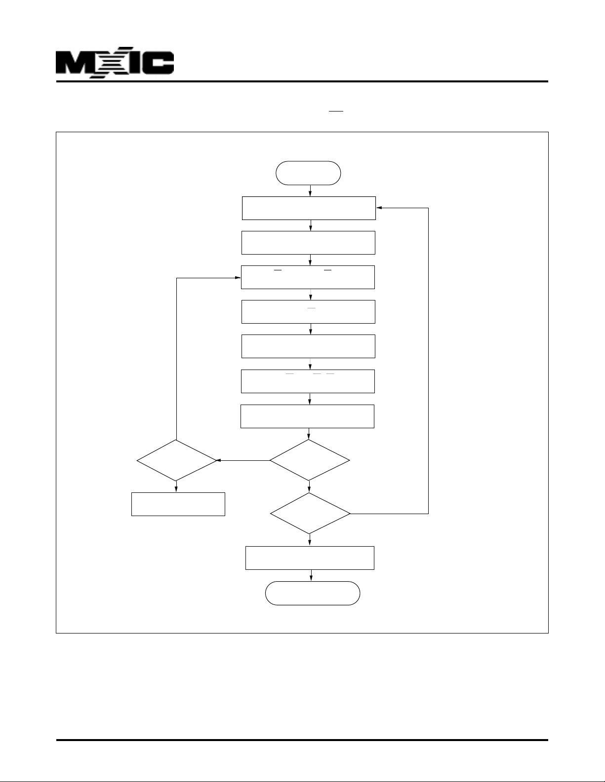
Please refer to sector protect algorithm and waveform.
T o v erify programming of the protection circuitry , the programming equipment must force VID on address pin A9
( with CE and OE at VIL and WE at VIH). When A1=VIH,
A0=VIL, A6=VIL, it will produce a logical "1" code at
device output Q0 f or a protected sector . Otherwise the
device will produce 00H for the unprotected sector. In
this mode, the addresses,except for A1, are don't care.
Address locations with A1 = VIL are reserved to read
manufacturer and device codes.(Read Silicon ID)
It is also possible to determine if the sector is protected
in the system by writing a Read Silicon ID command.
Perf orming a read operation with A1=VIH, it will produce
a logical "1" at Q0 for the protected sector .
P/N:PM0732
REV. 1.1, SEP. 19, 2001
16
Page 17

CHIP UNPROTECT
The MX29LV004T/B also features the chip unprotect
mode, so that all sectors are unprotected after chip
unprotect is completed to incorporate any changes in the
code. It is recommended to protect all sectors before
activating chip unprotect mode.
To activate this mode, the programming equipment must
force VID on control pin OE and address pin A9. The CE
pins must be set at VIL. Pins A6 must be set to VIH.(see
Table 2) Refer to chip unprotect algorithm and waveform
for the chip unprotect algorithm. The unprotection
mechanism begins on the falling edge of the WE pulse
and is terminated on the rising edge.
It is also possible to determine if the chip is unprotected
in the system by writing the Read Silicon ID command.
Performing a read operation with A1=VIH, it will produce
00H at data outputs(Q0-Q7) for an unprotected sector.
MX29LV004T/B
It is noted that all sectors are unprotected after the chip
unprotect algorithm is completed.
P/N:PM0732
REV. 1.1, SEP. 19, 2001
17
Page 18

ABSOLUTE MAXIMUM RATINGS
Storage T emperature
Plastic Packages . . . . . . . . . . . . . ..... -65oC to +150oC
Ambient T emperature
with Power Applied. . . . . . . . . . . . . .... -65oC to +125oC
V oltage with Respect to Ground
VCC (Note 1) . . . . . . . . . . . . . . . . . -0.5 V to +4.0 V
A9, OE, and
RESET (Note 2) . . . . . . . . . . . ....-0.5 V to +12.5 V
All other pins (Note 1) . . . . . . . -0.5 V to VCC +0.5 V
Output Short Circuit Current (Note 3) . . . . . . 200 mA
Notes:
1. Minimum DC voltage on input or I/O pins is -0.5 V.
During voltage transitions, input or I/O pins may overshoot VSS to -2.0 V for periods of up to 20 ns. See
Figure 6. Maximum DC voltage on input or I/O pins is
VCC +0.5 V. During voltage transitions, input or I/O
pins may overshoot to VCC +2.0 V for periods up to
20 ns. See Figure 7.
2. Minimum DC input voltage on pins A9, OE, and
RESET is -0.5 V. During voltage tr ansitions , A9, OE,
and RESET may ov ershoot VSS to -2.0 V f or periods
of up to 20 ns. See Figure 6. Maximum DC input voltage on pin A9 is +12.5 V which ma y overshoot to 14.0
V for periods up to 20 ns. The RESET pin is provided
for 40-pin TSOP package type.
3. No more than one output may be shorted to ground at
a time. Duration of the short circuit should not be
greater than one second.
MX29LV004T/B
OPERATING RATINGS
Commercial (C) Devices
Ambient Temperature (T
Industrial (I) Devices
Ambient Temperature (T
V
CC Supply Voltages
CC for full voltage range. . . . . . . . . . . +2.7 V to 3.6 V
V
V
CC for 55ns speed grade . . . . . . . . . . 3.3V ± 5%
Operating ranges define those limits between which the
functionality of the device is guaranteed.
A ). . . . . . . . . . . . 0 °C to +70°C
A ) . . . . . . . . . . -4 0 °C to +85 °C
Stresses above those listed under "Absolute Maximum
Rat-ings" may cause permanent damage to the device.
This is a stress rating only; functional operation of the
device at these or any other conditions above those indicated in the operational sections of this data sheet is
not implied. Exposure of the device to absolute maximum rating conditions for extended periods may affect
device reliability.
P/N:PM0732
REV. 1.1, SEP. 19, 2001
18
Page 19
MX29LV004T/B
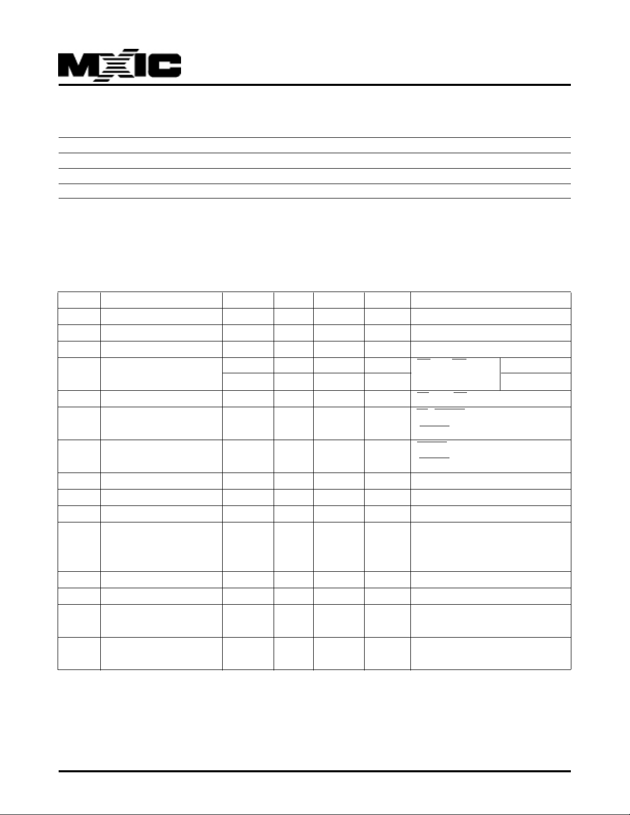
Table 8. CAPACITANCE TA = 25oC, f = 1.0 MHz
SYMBOL PARAMETER MIN. TYP MAX. UNIT CONDITIONS
CIN1 Input Capacitance 8 pF VIN = 0V
CIN2 Control Pin Capacitance 1 2 pF VIN = 0V
COUT Output Capacitance 12 pF VOUT = 0V
READ OPERATION
Table 9. DC CHARACTERISTICS TA = -40oC TO 85oC, VCC = 2.7V to 3.6V
(TA = 0oC TO 70oC, VCC = 3.3V
Symbol PARAMETER MIN. TYP MAX. UNIT CONDITIONS
ILI Input Leakage Current ± 1 uA VIN = VSS to VCC
ILIT A9 Input Leakage Current 35 uA VCC=VCC max; A9=12.5V
ILO Output Leakage Current ± 1 uA VOUT = VSS to VCC, VCC=VCC max
ICC1 VCC Active Read Currect 7 1 2 mA CE=VIL, OE=VIH @5MHz
2 4 mA @1MHz
ICC2 VCC Active write Currect 15 3 0 mA CE=VIL, OE=VIH
ICC3 VCC Standby Currect 0.2 5 u A CE; RESET=VCC ± 0.3V
ICC4 VCC Standby Currect 0.2 5 u A RESET=VSS ± 0.3V
During Reset (RESET pin for 40-TSOP)
ICC5 Automative sleep mode 0 .2 5 uA VIH=VCC ± 0.3V;VIL=VSS ± 0.3V
VIL Input Low Voltage(Note 1) -0.5 0.8 V
VIH Input High Voltage 0.7xVCC VCC+ 0.3 V
VID Voltage for Automative
Select and Temporary 11.5 12.5 V VCC=3.3V
Chip Unprotect
VOL Output Low Voltage 0.45 V IOL = 4.0mA, VCC= VCC min
VOH1 Output High Voltage(TTL) 0.85xVCC IOH = -2mA, VCC=VCC min
VOH2 Output High Voltage VCC-0.4 IOH = -100uA, VCC min
(CMOS)
VLKO Low VCC Lock-out 2.3 2.5 V
Voltage
±±
± 5% for MX29LV004T/B-55R)
±±
(RESET pin for 40-TSOP)
NOTES:
1.VIL min. = -1.0V for pulse width is equal to or less than 50 ns.
VIL min. = -2.0V for pulse width is equal to or less than 20 ns.
2.VIH max. = VCC + 1.5V for pulse width is equal to or less than 20 ns
If VIH is over the specified maximum value, read operation cannot be guaranteed.
3. Automatic sleep mode enable the low power mode when addresses remain stable for tACC +30ns.
P/N:PM0732
19
REV. 1.1, SEP. 19, 2001
Page 20
MX29LV004T/B
AC CHARACTERISTICS TA = -40oC to 85oC, VCC = 2.7V~3.6V
(TA = 0oC to 70oC, VCC = 3.3V
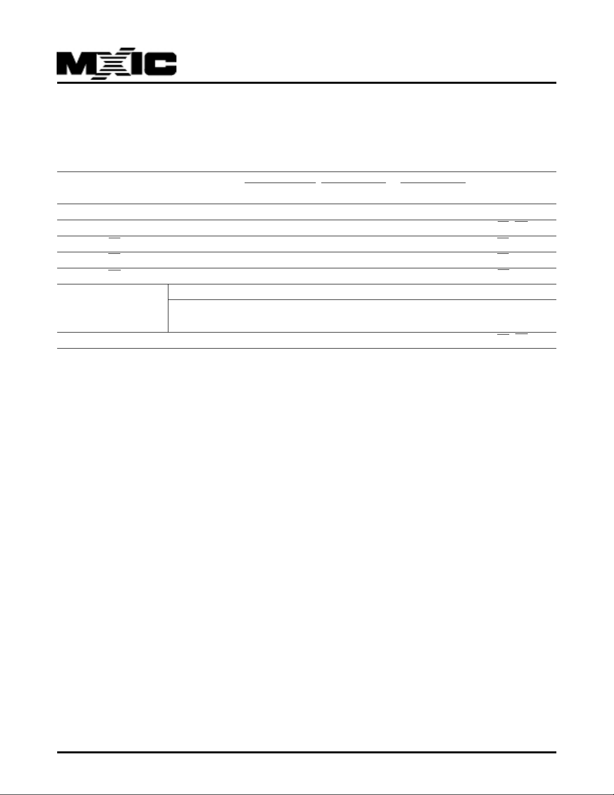
Table 10. READ OPERATIONS
29LV004T/B-55R 29LV004T/B-70 29LV004T/B-90
SYMBOL PARAMETER MIN. MAX. MIN. MAX. MIN. MAX. UNIT CONDITIONS
tRC Read Cycle Time (Note 1) 5 5 70 90 ns
tACC Address to Output Delay 55 70 90 ns CE=OE=VIL
tCE CE to Output Delay 55 70 90 ns OE=VIL
tOE OE to Output Delay 30 30 35 ns CE=VIL
tDF OE High to Output Float (Note1) 0 2 5 0 25 0 3 0 n s CE=VIL
tOEH Output Enable Read 0 0 0 ns
Hold Time Toggle and 10 10 10 ns
Data Polling
tOH Address to Output hold 0 0 0 ns CE=OE=VIL
±±
±5% for MX29LV004T/B-55R)
±±
TEST CONDITIONS:
• Input pulse levels: 0V/3.0V.
• Input rise and fall times is equal to or less than 5ns.
• Output load: 1 TTL gate + 100pF (Including scope and
jig), for 29LV004T/B-90. 1 TTL gate + 30pF (Including
scope and jig) for 29LV004T/B-70 & 29LV004T/B-55R.
• Reference levels for measuring timing: 1.5V.
NOTE:
1. Not 100% tested.
2. tDF is defined as the time at which the output achieves
the open circuit condition and data is no longer driven.
P/N:PM0732
REV. 1.1, SEP. 19, 2001
20
Page 21
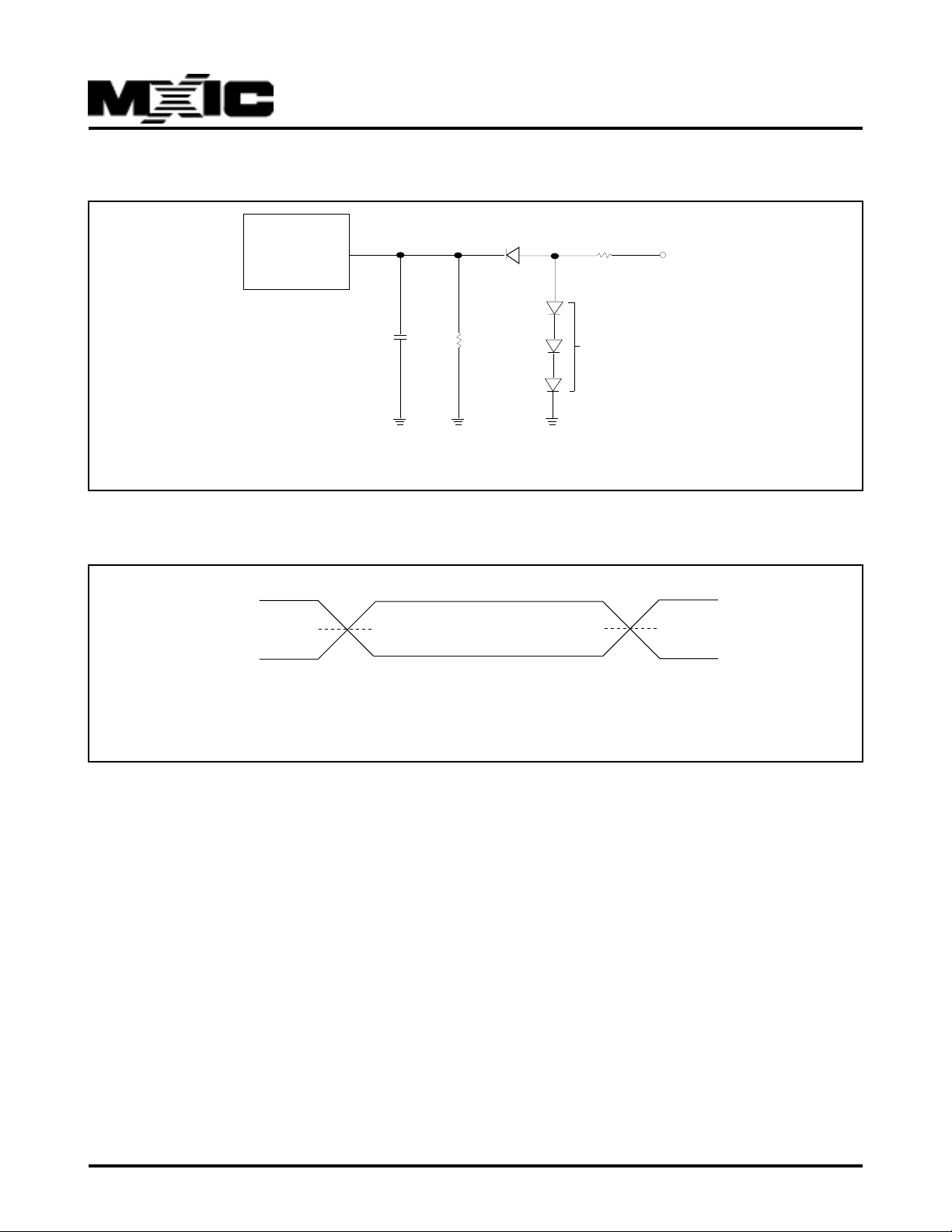
Figure 1. SWITCHING TEST CIRCUITS
MX29LV004T/B
DEVICE UNDER
TEST
CL=100pF Including jig capacitance
CL=30pF for MX29LV004T/B-70 & MX29LV004T/B-55R
Figure 2. SWITCHING TEST WAVEFORMS
3.0V
0V
INPUT
CL
TEST POINTS
6.2K ohm
2.7K ohm
DIODES=IN3064
OR EQUIVALENT
OUTPUT
+3.3V
1.5V1.5V
AC TESTING: Inputs are driven at 3.0V for a logic "1" and 0V for a logic "0".
Input pulse rise and fall times are < 5ns.
P/N:PM0732
REV. 1.1, SEP. 19, 2001
21
Page 22
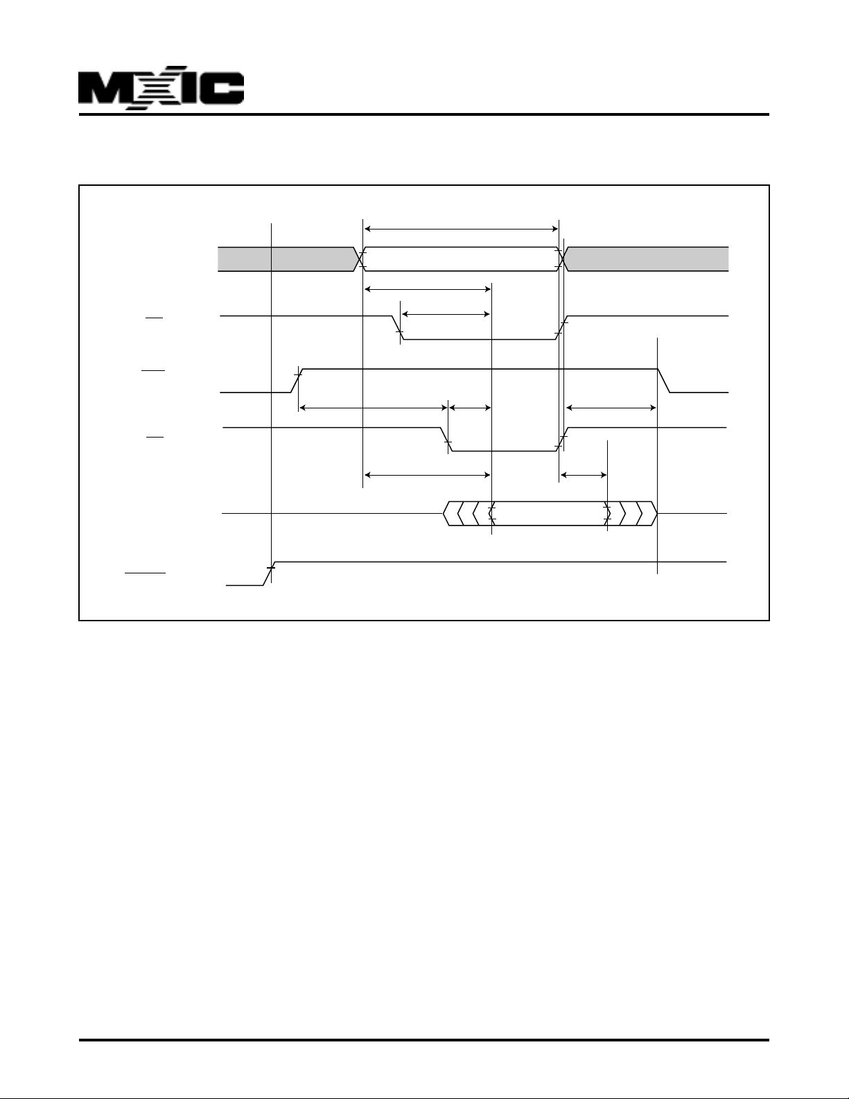
Figure 3. READ TIMING WAVEFORMS
MX29LV004T/B
tRC
Addresses
CE
WE
OE
Outputs
RESET
VIH
VIL
VIH
VIL
VIH
VIL
VIH
VIL
VOH
VOL
VIH
VIL
HIGH Z
tOEH
tACC
tACC
ADD Valid
tCE
tOE
DATA V alid
tDF
tOH
HIGH Z
P/N:PM0732
REV. 1.1, SEP. 19, 2001
22
Page 23

MX29LV004T/B
AC CHARACTERISTICS TA = -40oC to 85oC, VCC = 2.7V~3.6V
(TA = 0oC to 70oC, VCC = 3.3V
Table 11. Erase/Program Operations
29LV004T/B-55R 29LV004T/B-70 29LV004T/B-90
SYMBOL PARAMETER MIN. MAX. MIN. MAX. MIN. MAX. UNIT
tW C Write Cycle Time (Note 1) 55 70 9 0 ns
tAS Address Setup Time 0 0 0 ns
tAH Address Hold Time 45 45 4 5 ns
tDS Data Setup Time 35 35 45 ns
tD H Data Hold Time 0 0 0 ns
tOES Output Enable Setup Time 0 0 0 ns
tGHWL Read Recovery Time Before 0 0 0 ns
Write (OE High to WE Low)
tCS CE Setup Time 0 0 0 ns
±±
±5% for MX29LV004T/B-55R)
±±
tC H CE Hold Time 0 0 0 ns
tWP Write Pulse Width 3 5 3 5 35 ns
tWPH Write Pulse Width High 30 30 30 ns
tWHWH1 Programming Operation (Note 2) 9(Typ.) 9(Typ.) 9(Typ.) us
(Byte program time)
tWHWH2 Sector Erase Operation (Note 2) 0.7(Typ.) 0.7(Typ.) 0.7(Typ.) sec
tVCS VCC Setup Time (Note 1) 5 0 50 50 us
tRB(Note3)Recovery Time from RY/BY 0 0 0 ns
tBUSY Program/Erase Vaild to RY/BY 90 90 90 ns
(Note 3) Delay
tWPP1 Write pulse width for sector 100ns 10us 100ns 10us 100ns 10us
protect (A9, OE Control) (Typ.) (Typ.) (Typ.)
tWPP2 Write pulse width for sector 100ns 12ms 100ns 12ms 100ns 12ms
protect (A9, OE Control) (Typ.) (Typ.) (Typ.)
NOTES:
1. Not 100% tested.
2. See the "Er ase and Programming P erformance" section for more information.
3. RY/BY pin is provided for 40-TSOP.
P/N:PM0732
REV. 1.1, SEP. 19, 2001
23
Page 24

MX29LV004T/B
AC CHARACTERISTICS T A = -40
(T A = 0oC to 70oC, VCC = 3.3V
o
C to 85oC, VCC = 2.7V~3.6V
±±
±5% f or MX29LV004T/B-55R)
±±
Table 12. Alternate CE Controlled Erase/Program Operations
29LV004T/B-55R 29LV004T/B-70 29LV004T/B-90
SYMBOL PARAMETER MIN. MAX. MIN. MAX. MIN. MAX. UNIT
tW C Write Cycle Time (Note 1) 55 70 70 ns
tAS Address Setup Time 0 0 0 ns
tAH Address Hold Time 45 4 5 4 5 ns
tDS Data Setup Time 35 3 5 45 ns
tDH Data Hold Time 0 0 0 ns
tOES Output Enable Setup Time 0 0 0 ns
tGHEL Read Recovery Time Before Write 0 0 0 ns
tWS WE Setup Time 0 0 0 n s
tWH WE Hold Time 0 0 0 ns
tCP CE Pulse Width 35 35 35 ns
tCPH CE Pulse Width High 30 3 0 30 ns
tWHWH1 Programming Operation(note2) 9(Typ .) 9(T yp.) 9(T yp.) us
tWHWH2 Sector Erase Operation (note2) 0.7(T yp .) 0.7(Typ .) 0.7(T yp.) sec
NOTE:
1. Not 100% tested.
2. See the "Er ase and Programming P erformance" section for more information.
P/N:PM0732
REV. 1.1, SEP. 19, 2001
24
Page 25
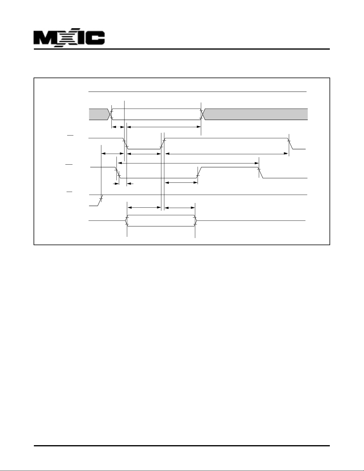
Figure 4. COMMAND WRITE TIMING WAVEFORM
MX29LV004T/B
VCC
Addresses
WE
CE
OE
Data
VIH
VIL
VIH
VIL
VIH
VIL
VIH
VIL
VIH
VIL
3V
ADD Valid
tAS
tOES
tCS tCH
tWP
tDS
tAH
tWPH
tCWC
tDH
DIN
P/N:PM0732
REV. 1.1, SEP. 19, 2001
25
Page 26
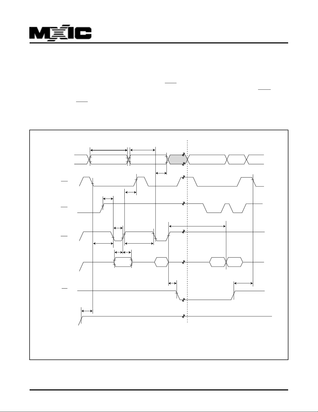
AUTOMATIC PROGRAMMING TIMING
WAVEFORM
MX29LV004T/B
One byte data is programmed. Verify in fast algorithm
and additional verification by external control are not required because these operations are executed automatically by internal control circuit. Programming comple-
after automatic programming starts. Device outputs
DAT A during programming and DAT A after programming
on Q7.(Q6 is for toggle bit; see toggle bit, D AT A polling,
timing waveform)
tion can be verified by D A T A polling and toggle bit checking
Figure 5. AUTOMATIC PROGRAMMING TIMING WAVEFORM
Address
CE
OE
tWC
555h
tGHWL
tWP
tAS
PA
tAH
tCH
Read Status Data (last two cycle)Program Command Sequence(last two cycle)
PA PA
tWHWH1
WE
Data
RY/BY
VCC
tCS tWPH
tDS tDH
A0h
tVCS
NOTES:
1.PA=Program Address, PD=Program Data, DOUT is the true data the program address
PD
tBUSY
Status
DOUT
tRB
P/N:PM0732
REV. 1.1, SEP. 19, 2001
26
Page 27
MX29LV004T/B
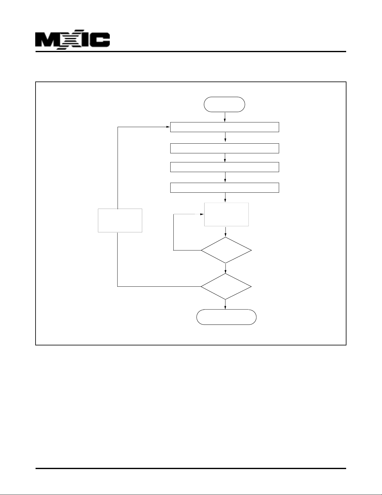
Figure 6. AUTOMATIC PROGRAMMING ALGORITHM FLOWCHART
START
Write Data AAH Address 555H
Write Data 55H Address 2AAH
Write Data A0H Address 555H
Write Program Data/Address
Increment
Address
No
No
Verify Word Ok ?
Last Address ?
Auto Program Completed
Data Poll
from system
YES
YES
P/N:PM0732
REV. 1.1, SEP. 19, 2001
27
Page 28
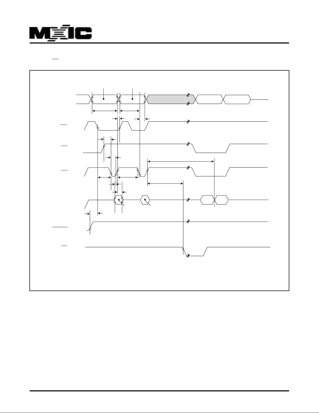
Figure 7. CE CONTROLLED PR OGRAM TIMING W A VEFORM
MX29LV004T/B
Address
WE
OE
CE
Data
555 for program
2AA for erase
tWC
tWH
tGHEL
tWS
tRH
PA for program
SA for sector erase
555 for chip erase
tCP
tDS
tDH
tAS
tAH
tCPH
A0 for program
55 for erase
Data Polling
tBUSY
PD for program
30 for sector erase
10 for chip erase
tWHWH1 or 2
DQ7
PA
DOUT
RESET
RY/BY
NOTES:
1.PA=Program Address, PD=Program Data, DOUT=Data Out, DQ7=complement of data written to device.
2.Figure indicates the last two bus cycles of the command sequence.
P/N:PM0732
REV. 1.1, SEP. 19, 2001
28
Page 29
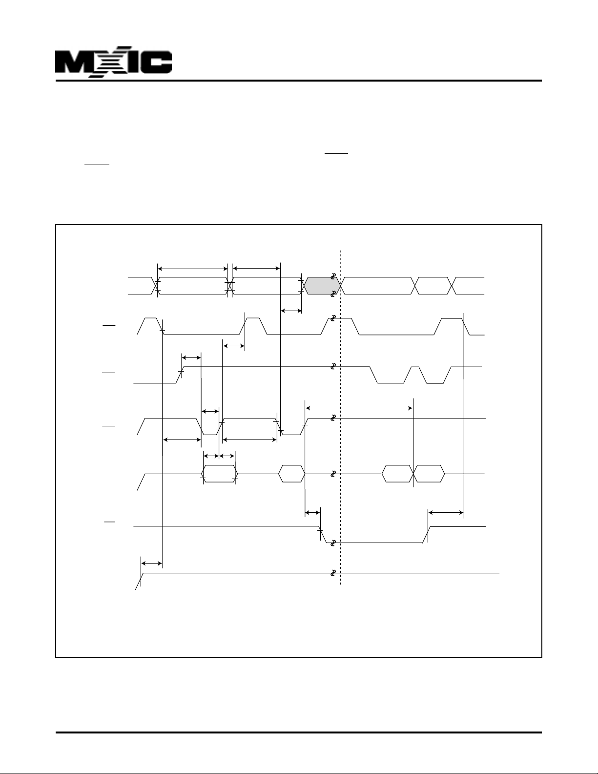
AUTOMATIC CHIP ERASE TIMING WAVEFORM
MX29LV004T/B
All data in chip are erased. External erase verification is
not required because data is verified automatically by
internal control circuit. Erasure completion can be veri-
matic erase starts. Device outputs 0 during erasure
and 1 after erasure on Q7.(Q6 is for toggle bit; see toggle
bit, DAT A polling, timing wav eform)
fied by DATA polling and toggle bit checking after auto-
Figure 8. AUTOMATIC CHIP ERASE TIMING WAVEFORM
Address
CE
OE
tWC
2AAh
tGHWL
tWP
tAS
555h
tAH
tCH
Read Status Data Erase Command Sequence(last two cycle)
VA VA
tWHWH2
WE
Data
RY/BY
VCC
tCS tWPH
tDS tDH
In
Progress
Complete
tRB
tVCS
55h
10h
tBUSY
NOTES:
SA=sector address(for Sector Erase), VA=Valid Address for reading status data(see "Write Operation Status").
P/N:PM0732
REV. 1.1, SEP. 19, 2001
29
Page 30
MX29LV004T/B
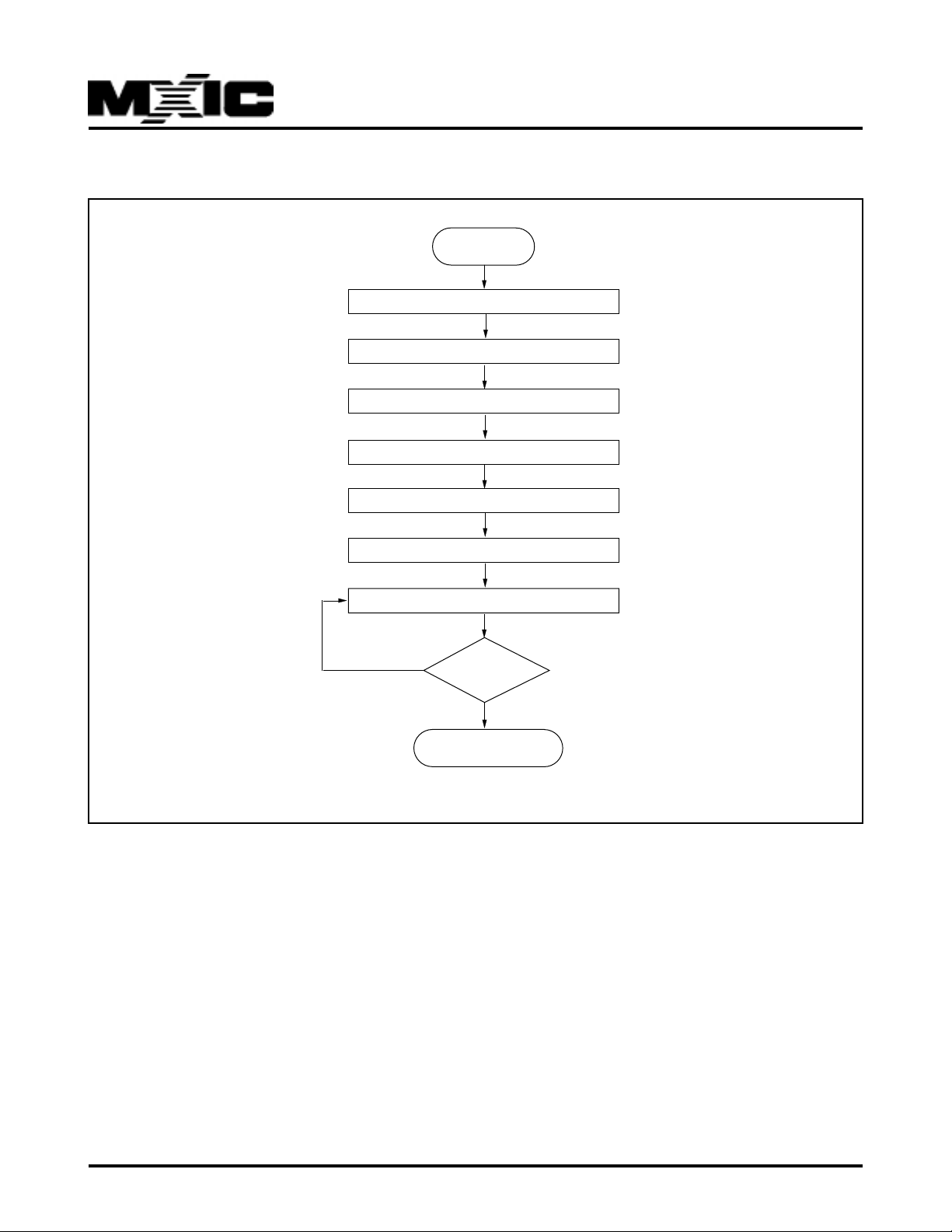
Figure 9. AUTOMATIC CHIP ERASE ALGORITHM FLOWCHART
START
Write Data AAH Address 555H
Write Data 55H Address 2AAH
Write Data 80H Address 555H
Write Data AAH Address 555H
Write Data 55H Address 2AAH
Write Data 10H Address 555H
NO
Data Pall from System
Data=FFh ?
YES
Auto Chip Erase Completed
P/N:PM0732
REV. 1.1, SEP. 19, 2001
30
Page 31
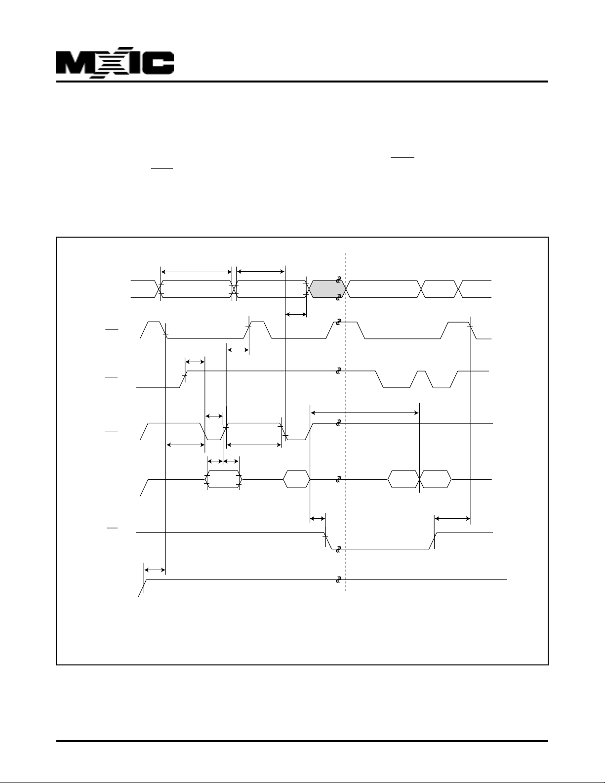
AUTOMATIC SECTOR ERASE TIMING WAVEFORM
MX29LV004T/B
Sector indicated by A12 to A17 are erased. External
erase verify is not required because data are verified
automatically by internal control circuit. Erasure comple-
ing after automatic erase starts. De vice outputs 0 during erasure and 1 after erasure on Q7.(Q6 is for toggle
bit; see toggle bit, D AT A polling, timing wa vef orm)
tion can be verified by DAT A polling and toggle bit check-
Figure 10. AUTOMATIC SECTOR ERASE TIMING WAVEFORM
Read Status Data Erase Command Sequence(last two cycle)
Address
CE
OE
tWC
2AAh
tGHWL
tWP
tAS
SA
tAH
tCH
tWHWH2
VA VA
WE
Data
RY/BY
VCC
tCS tWPH
tDS tDH
In
Progress
Complete
tRB
tVCS
55h
30h
tBUSY
NOTES:
SA=sector address(for Sector Erase), VA=Valid Address for reading status data(see "Write Operation Status").
P/N:PM0732
REV. 1.1, SEP. 19, 2001
31
Page 32
MX29LV004T/B
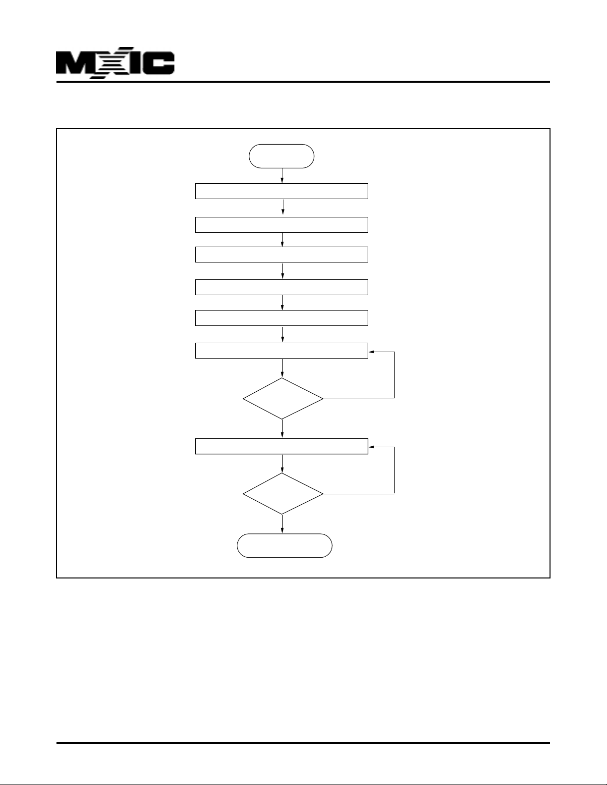
Figure 11. AUTOMATIC SECTOR ERASE ALGORITHM FLOWCHART
START
Write Data AAH Address 555H
Write Data 55H Address 2AAH
Write Data 80H Address 555H
Write Data AAH Address 555H
Write Data 55H Address 2AAH
Write Data 30H Sector Address
Last Sector
to Erase
YES
Data Poll from System
Data=FFh
YES
Auto Sector Erase Completed
NO
NO
P/N:PM0732
REV. 1.1, SEP. 19, 2001
32
Page 33
MX29LV004T/B
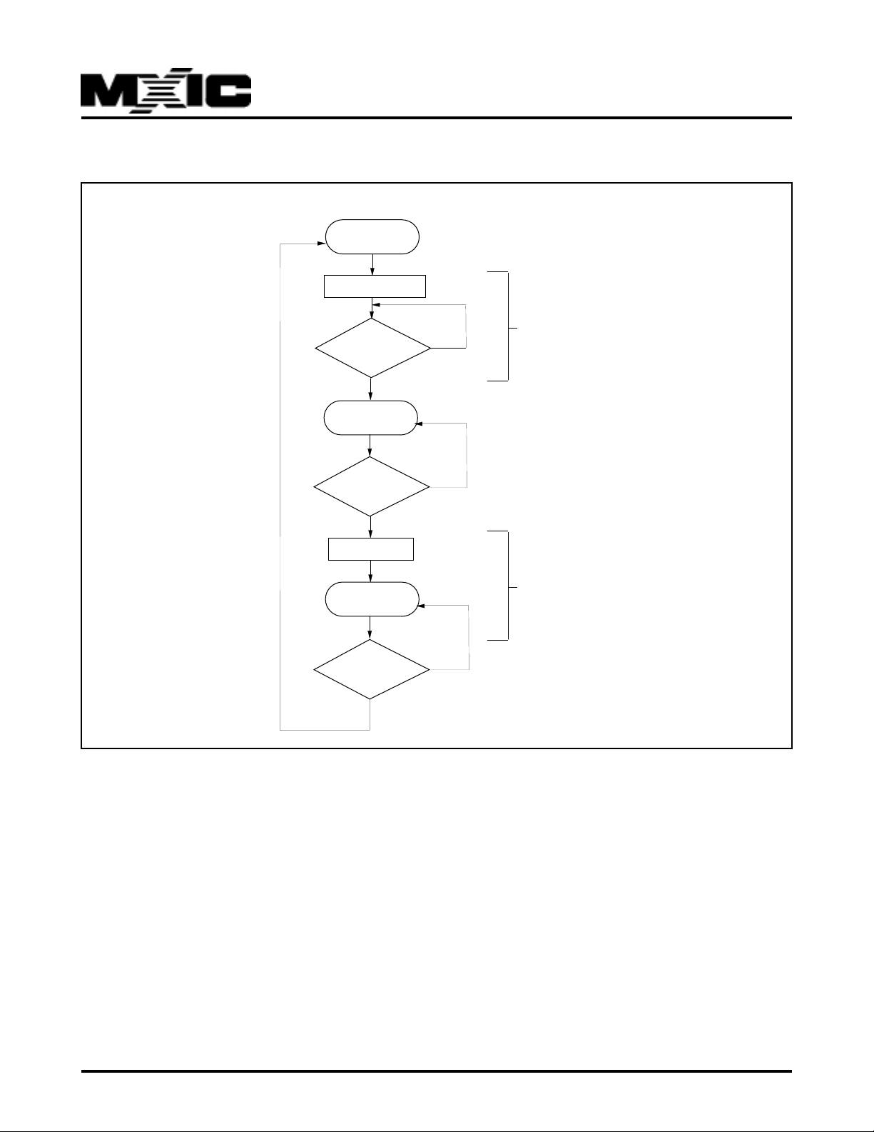
Figure 12. ERASE SUSPEND/ERASE RESUME FLOWCHART
START
Write Data B0H
Toggle Bit checking Q6
not toggled
YES
Read Array or
Program
Reading or
Programming End
YES
Write Data 30H
Continue Erase
Another
Erase Suspend ?
YES
NO
NO
NO
ERASE SUSPEND
ERASE RESUME
P/N:PM0732
REV. 1.1, SEP. 19, 2001
33
Page 34
MX29LV004T/B
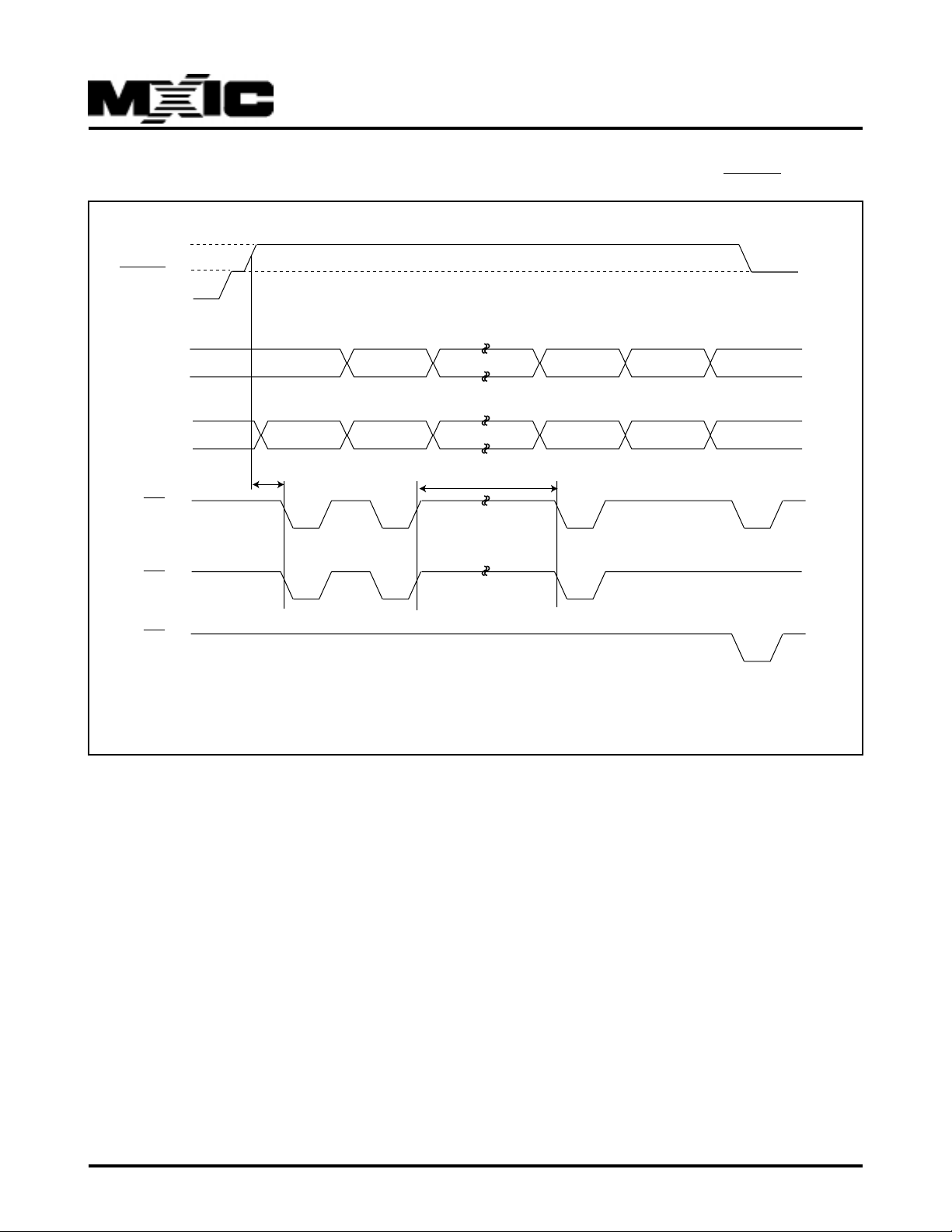
Figure 13. IN-SYSTEM SECTOR PROTECT/UNPROTECT TIMING WAVEFORM (RESET Control)
VID
RESET
SA, A6
A1, A0
Data
CE
WE
OE
VIH
Valid*
Sector Protect or Sector Unprotect
Valid* Valid*
Verify
40h60h60h
1us
Sector Protect =150us
Sector Unprotect =15ms
Note: When sector protect, A6=0, A1=1, A0=0. When sector unprotect, A6=1, A1=1, A0=0.
Status
P/N:PM0732
REV. 1.1, SEP. 19, 2001
34
Page 35
MX29LV004T/B
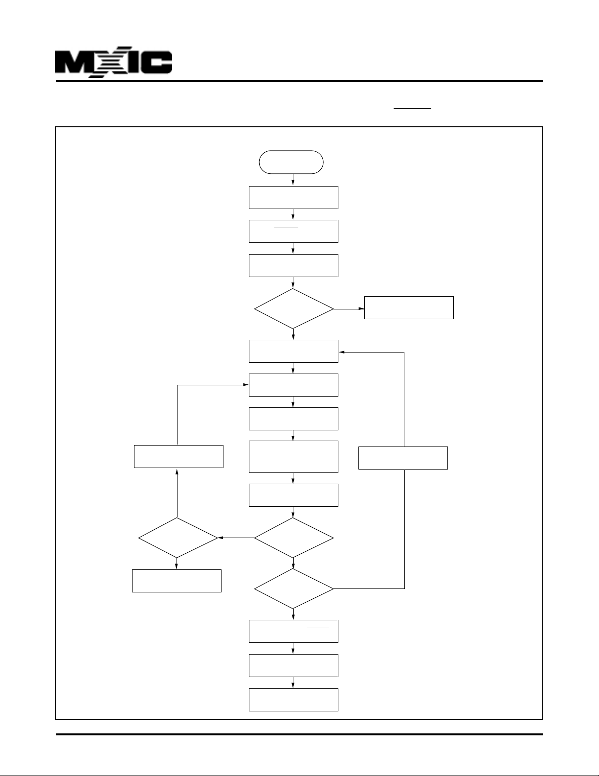
Figure 14. IN-SYSTEM SECTOR PROTECTION ALGORITHM WITH RESET=VID
START
PLSCNT=1
RESET=VID
Wait 1us
Increment PLSCNT
No
PLSCNT=25?
Yes
Device failed
First Write
Cycle=60H
Yes
Set up sector address
Write 60H to sector address
with A6=0, A1=1, A0=0
Wait 150us
Verify sector protect :
write 40H with A6=0,
A1=1, A0=0
Read from sector address
No
Data=01H
Yes
Protect another
sector?
No
?
Yes
Temporary Sector
Unprotect Mode
Reset PLSCNT=1
P/N:PM0732
No
Remove VID from RESET
Write reset command
Sector protect complete
REV. 1.1, SEP. 19, 2001
35
Page 36
MX29LV004T/B
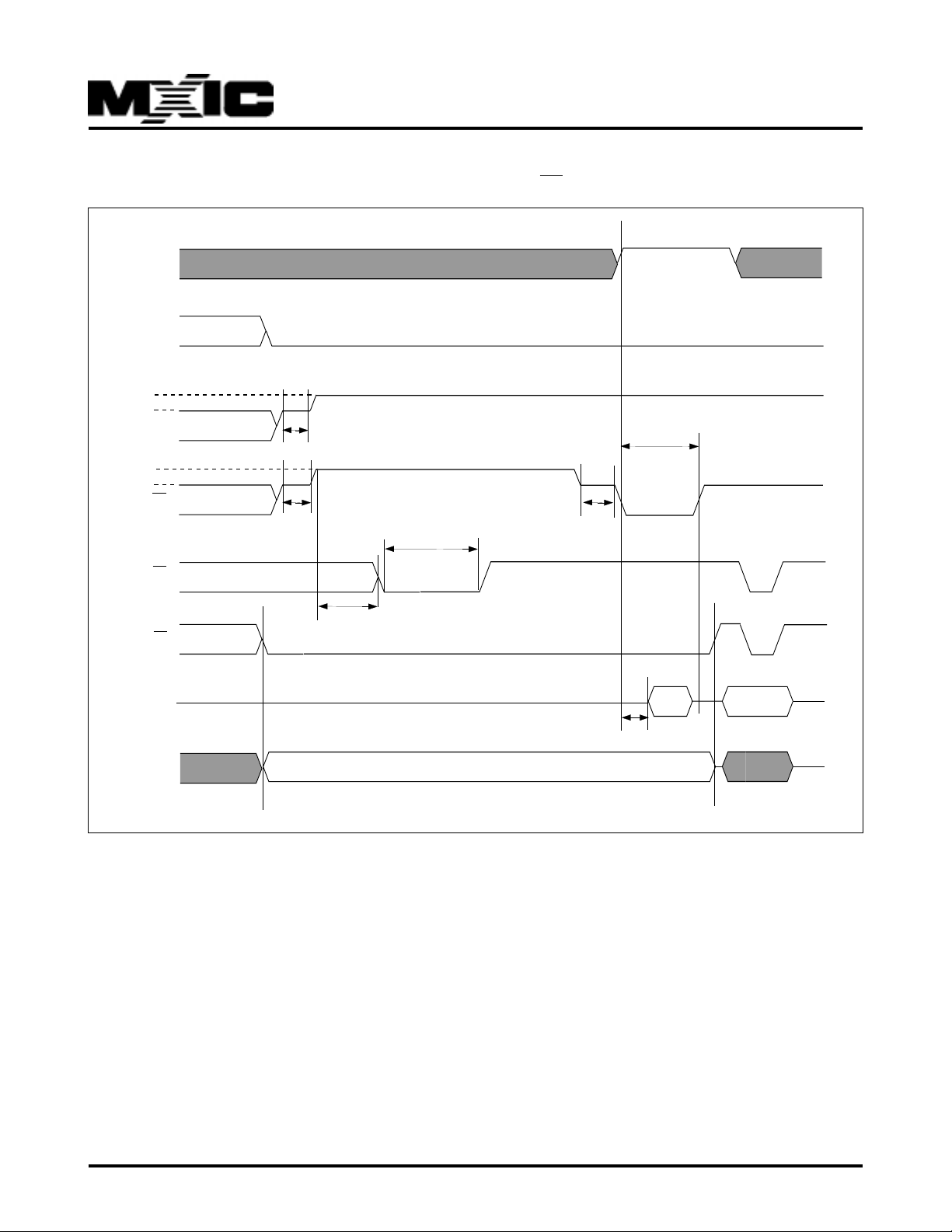
Figure 15. SECTOR PROTECT TIMING WAVEFORM(A9, OE Control)
A1
A6
12V
3V
A9
12V
3V
OE
tVLHT
tVLHT
tVLHT
tWPP 1
Verify
WE
CE
Data
A18-A12
tOESP
01H F0H
tOE
Sector Address
P/N:PM0732
REV. 1.1, SEP. 19, 2001
36
Page 37
MX29LV004T/B
Figure 16. SECTOR PROTECTION ALGORITHM (A9, OE Control)
START
Set Up Sector Addr
PLSCNT=1
OE=VID,A9=VID,CE=VIL
A6=VIL
Activate WE Pulse
Time Out 150us
No
PLSCNT=32?
Yes
Device Failed
No
Set WE=VIH, CE=OE=VIL
A9 should remain VID
Read from Sector
Addr=SA, A1=1
Data=01H?
Protect Another
Sector?
Remove VID from A9
Write Reset Command
Sector Protection
Complete
.
Yes
P/N:PM0732
REV. 1.1, SEP. 19, 2001
37
Page 38
MX29LV004T/B
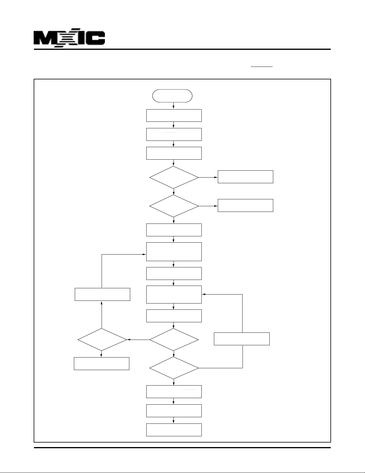
Figure 17. IN-SYSTEM SECTOR UNPROTECTION ALGORITHM WITH RESET=VID
START
PLSCNT=1
RESET=VID
Wait 1us
Increment PLSCNT
No
PLSCNT=1000?
First Write
Cycle=60H ?
All sector
protected?
Set up first sector address
Sector unprotect :
write 60H with
A6=1, A1=1, A0=0
Wait 50ms
Verify sector unprotect
write 40H to sector address
with A6=1, A1=1, A0=0
Read from sector address
with A6=1, A1=1, A0=0
No
Data=00H
Yes
Yes
No
No
?
Temporary Sector
Unprotect Mode
Protect all sectors
Set up next sector address
P/N:PM0732
Yes
Device failed
Yes
Last sector
verified?
No
Remove VID from RESET
Write reset command
Sector unprotect complete
38
Yes
REV. 1.1, SEP. 19, 2001
Page 39
MX29LV004T/B
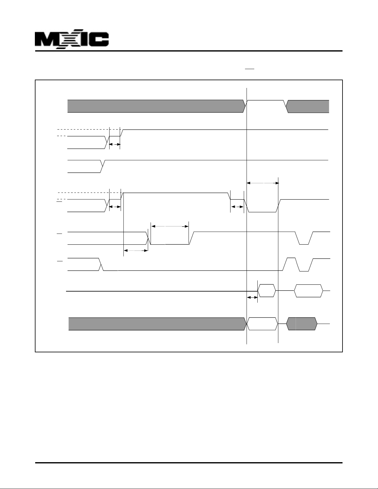
Figure 18. TIMING WAVEFORM FOR CHIP UNPROTECTION (A9, OE Control)
A1
12V
3V
A9
A6
tVLHT
12V
3V
OE
tVLHT
tWPP 2
tVLHT
WE
tOESP
CE
Data
A18-A12
Notes: tWPP1 (Write pulse width for sector protect)=100ns min, 10us(typ.).
tWPP2 (Write pulse width for sector unprotect)=100ns min, 12ms(typ).
Verify
00H
tOE
Sector Address
F0H
P/N:PM0732
REV. 1.1, SEP. 19, 2001
39
Page 40
MX29LV004T/B
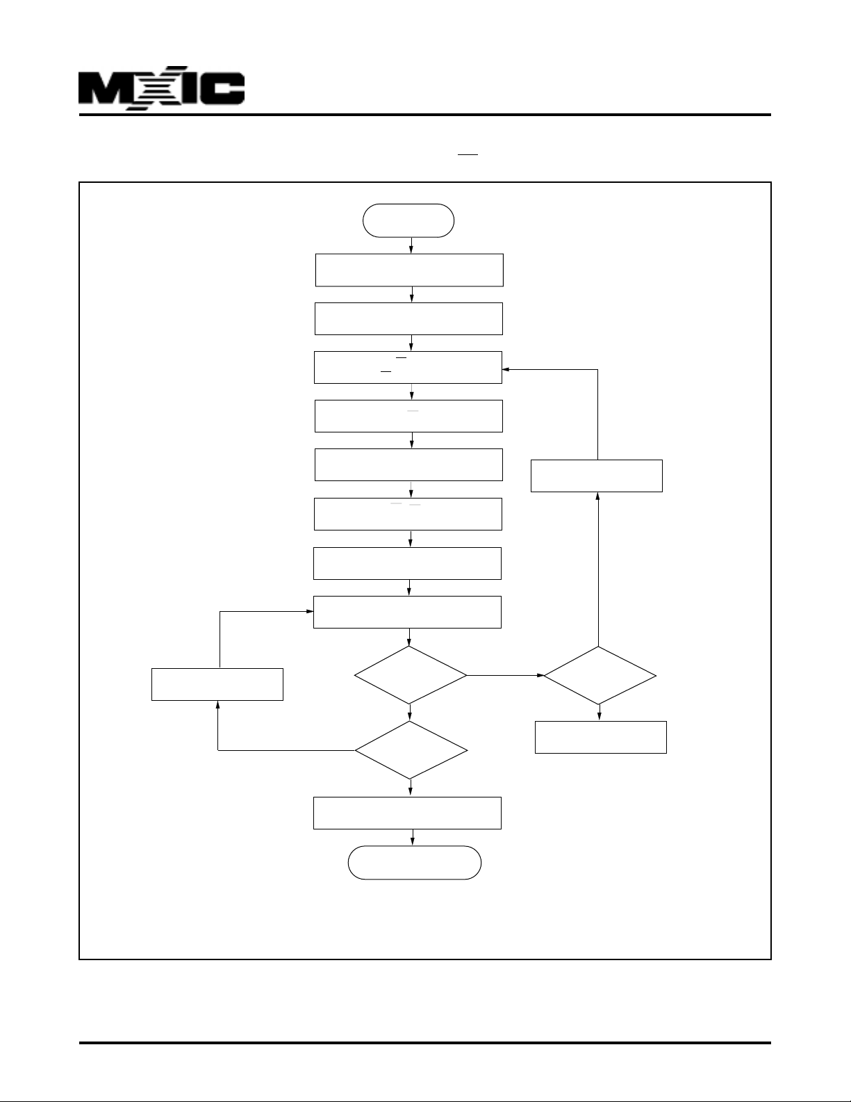
Figure 19. CHIP UNPROTECTION ALGORITHM (A9, OE Control)
START
Protect All Sectors
PLSCNT=1
Set OE=A9=VID
CE=VIL,A6=1
Activate WE Pulse
Increment
Sector Addr
Set Up First Sector Addr
Read Data from Device
No
Remove VID from A9
Write Reset Command
Time Out 50ms
Set OE=CE=VIL
A9=VID,A1=1
Data=00H?
Yes
All sectors have
been verified?
Yes
Chip Unprotect
Complete
No
Increment
PLSCNT
No
PLSCNT=1000?
Yes
Device Failed
P/N:PM0732
* It is recommended before unprotect whole chip, all sectors should be protected in advance.
REV. 1.1, SEP. 19, 2001
40
Page 41
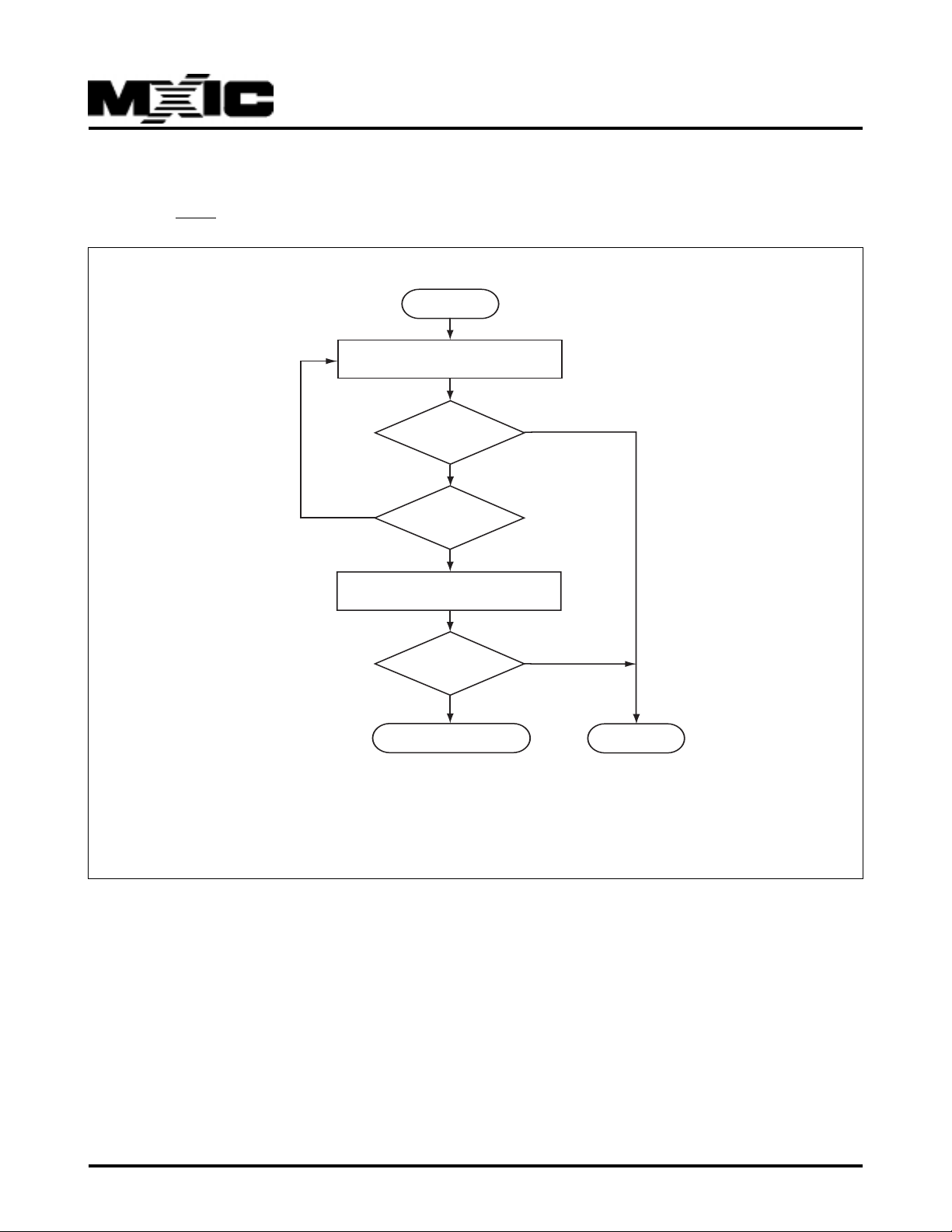
WRITE OPERATION STATUS
Figure 20. DATA POLLING ALGORITHM
Start
Read Q7~Q0
Add.=VA(1)
MX29LV004T/B
Q7 = Data ?
No
No
NOTE : 1.VA=Valid address for programming
2.Q7 should be re-checked even Q5="1" because Q7 may change
simultaneously with Q5.
Q5 = 1 ?
Yes
Read Q7~Q0
Add.=VA
Q7 = Data ?
No
FAIL
(2)
Yes
Yes
Pass
P/N:PM0732
REV. 1.1, SEP. 19, 2001
41
Page 42
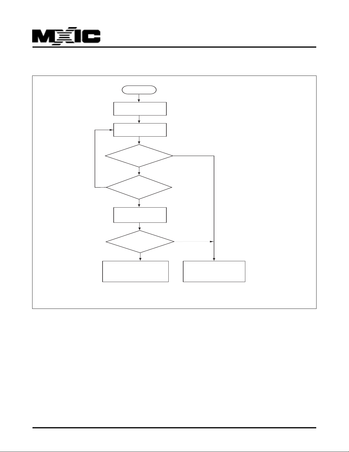
Figure 21. TOGGLE BIT ALOGRITHM
Start
Read Q7-Q0
MX29LV004T/B
Read Q7-Q0
Toggle Bit Q6 =
Toggle ?
YES
NO
Program/Erase Operation
Note:1.Read toggle bit twice to determine whether or not it is toggling.
2. Recheck toggle bit because it may stop toggling as Q5 change to "1".
Q5= 1?
YES
Read Q7~Q0 Twice
Toggle bit Q6=
Toggle?
YES
Not Complete,Write
Reset Command
(Note 1)
NO
(Note 1,2)
NO
Program/Erase
operation Complete
P/N:PM0732
REV. 1.1, SEP. 19, 2001
42
Page 43
MX29LV004T/B
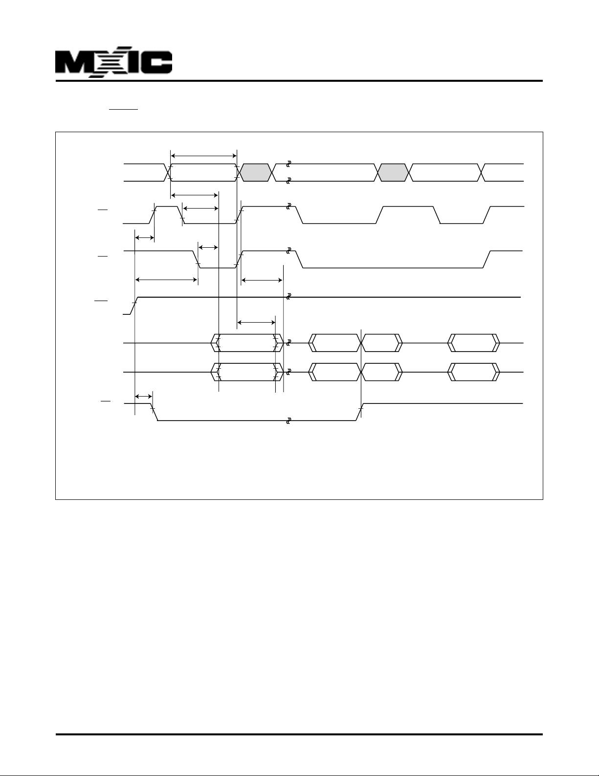
Figure 22. DATA POLLING TIMINGS (DURING AUTOMATIC ALOGRITHMS)
tRC
Address
tACC
tCE
VAVAVA
CE
tCH
tOE
OE
tOEH
tDF
WE
tOH
DQ7
Q0-Q6
Complement
Status Data
tBUSY
Complement
Status Data
Valid DataTrue
Valid DataTrue
RY/BY
NOTES:
VA=Valid address. Figure shows are first status cycle after command sequence, last status read cycle, and array data read cycle.
High Z
High Z
P/N:PM0732
REV. 1.1, SEP. 19, 2001
43
Page 44
MX29LV004T/B
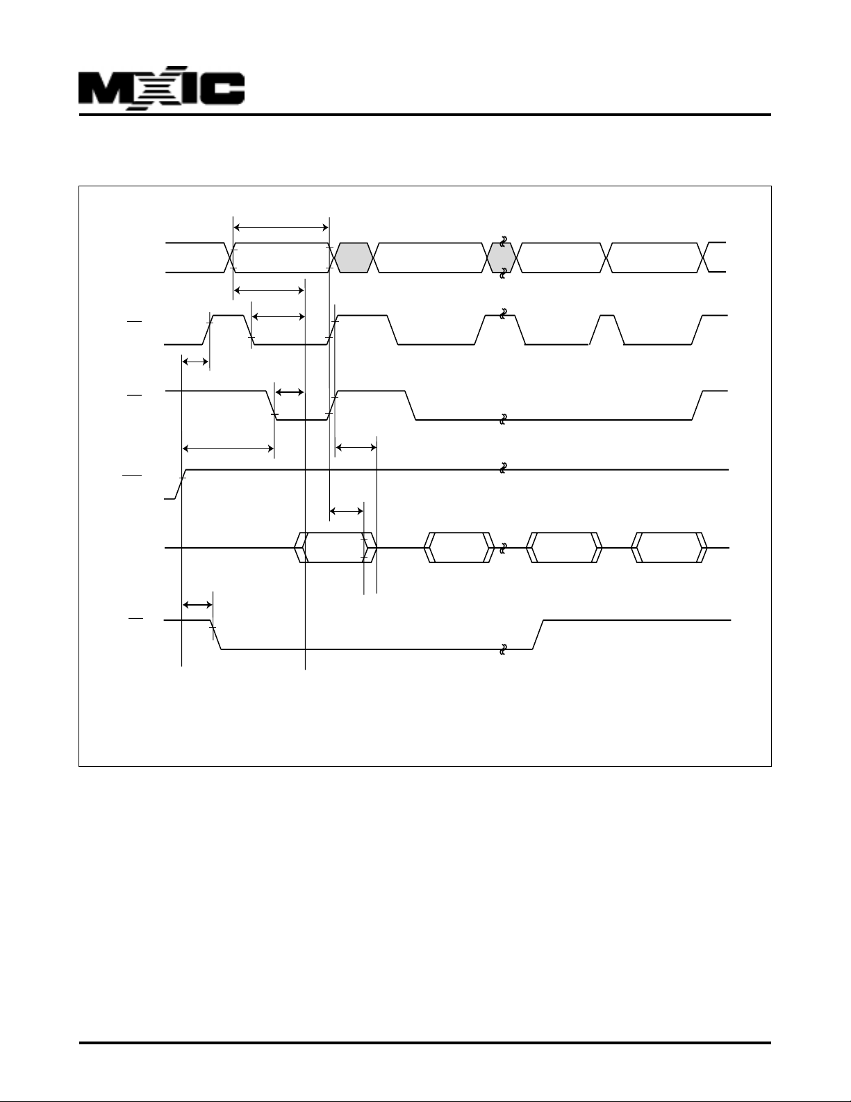
Figure 23. TOGGLE BIT TIMING WAVEFORMS (DURING AUTOMATIC ALOGRITHMS)
tRC
Address
CE
OE
WE
Q6/Q2
RY/BY
tCH
tBUSY
tOEH
High Z
tACC
VA
tCE
tOE
tDF
tOH
Valid Status
(first raed)
VA
Valid Status
(second read) (stops toggling)
VA
Valid Data
VA
Valid Data
P/N:PM0732
NOTES:
VA=Valid address; not required for Q6. Figure shows first two status cycle after command sequence, last status read cycle, and
array data read cycle.
REV. 1.1, SEP. 19, 2001
44
Page 45
MX29LV004T/B
Table 13. AC CHARACTERISTICS (for 40-pin TSOP package type)
Parameter Std Description Test Setup All Speed Options Unit
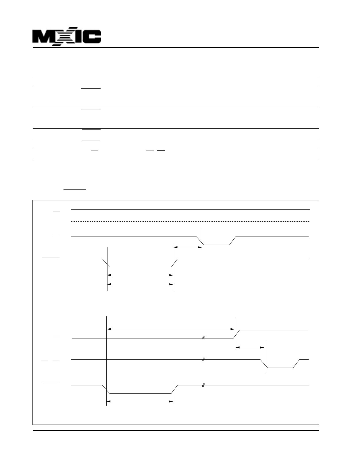
tREAD Y1 RESET PIN Low (During Automatic Algorithms) MAX 20 us
to Read or Write (See Note)
tREAD Y2 RESET PIN Low (NOT During Automatic MAX 50 0 ns
Algorithms) to Read or Write (See Note)
tRP RESET Pulse Width (During Automatic Algorithms) MIN 5 00 ns
tR H RESET High Time Before Read(See Note) MIN 50 ns
tRB RY/BY Recov ery Time(to CE, OE go low) MIN 0 ns
Note:Not 100% tested
Figure 24. RESET TIMING WAVFORM (for 40-pin TSOP package type)
RY/BY
CE, OE
RESET
RY/BY
CE, OE
tRH
tRP
tReady2
Reset Timing NOT during Automatic Algorithms
tReady1
tRB
RESET
P/N:PM0732
tRP
Reset Timing during Automatic Algorithms
REV. 1.1, SEP. 19, 2001
45
Page 46
MX29LV004T/B
Table 14. TEMPORARY SECTOR UNPROTECT
Parameter Std. Description T est Setup AllSpeed Options Unit
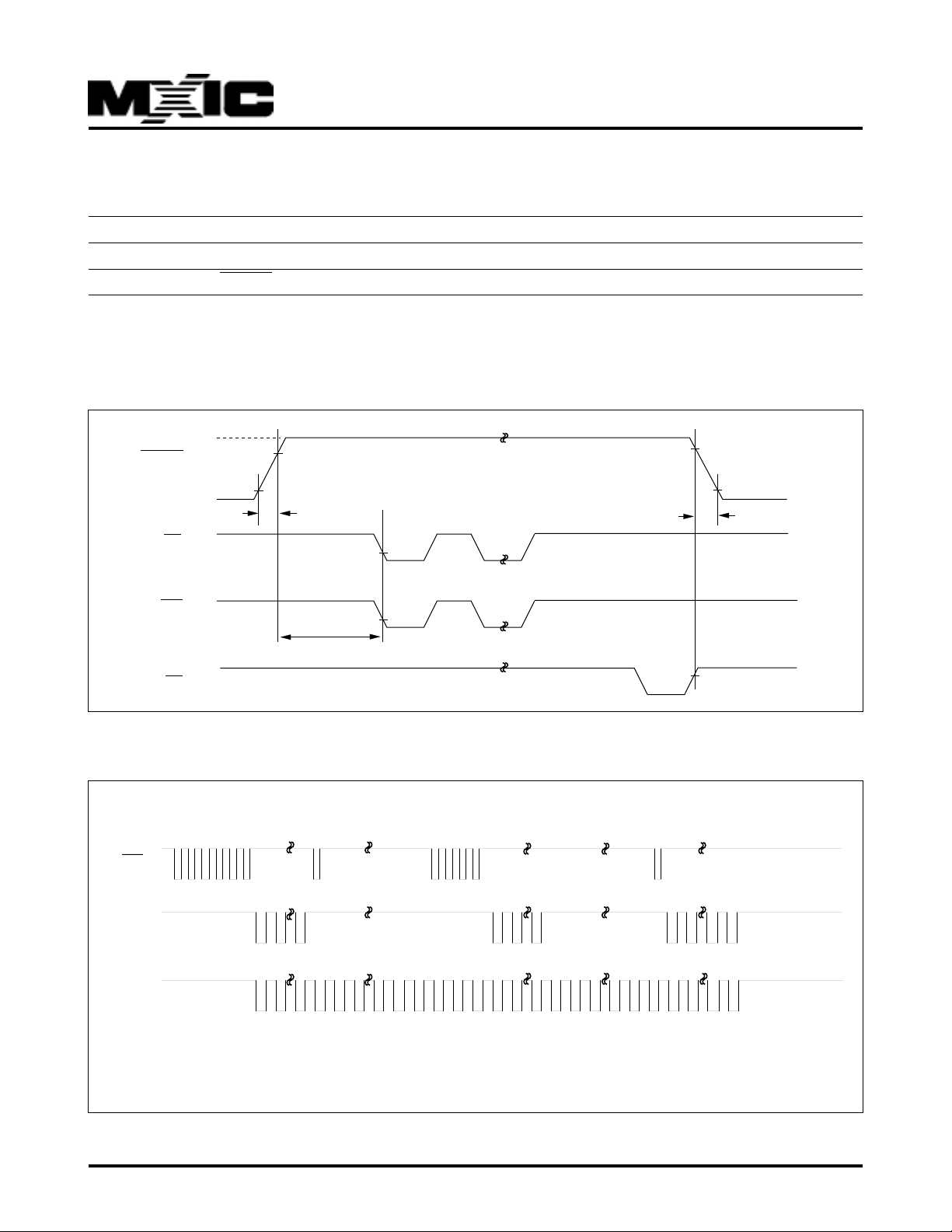
tVIDR VID Rise and Fall Time (See Note) Min 500 ns
tRSP RESET Setup Time for Temporary Sector Unprotect Min 4 us
Note:
Not 100% tested
Figure 25. TEMPORARY SECTOR UNPROTECT TIMING DIAGRAM
12V
RESET
0 or Vcc
tVIDR
CE
WE
tRSP
RY/BY
Program or Erase Command Sequence
Figure 26. Q6 vs Q2 for Erase and Erase Suspend Operations
Enter Embedded
Erasing
WE
Q6
Erase
Erase
Suspend
Enter Erase
Suspend Program
Erase
Suspend
Program
Erase Suspend
Read
Erase
Resume
tVIDR
Erase
0 or Vcc
Erase
Complete
Q2
P/N:PM0732
NOTES:
The system can use OE or CE to toggle Q2/Q6, Q2 toggles only when read at an address within an erase-suspended
REV. 1.1, SEP. 19, 2001
46
Page 47
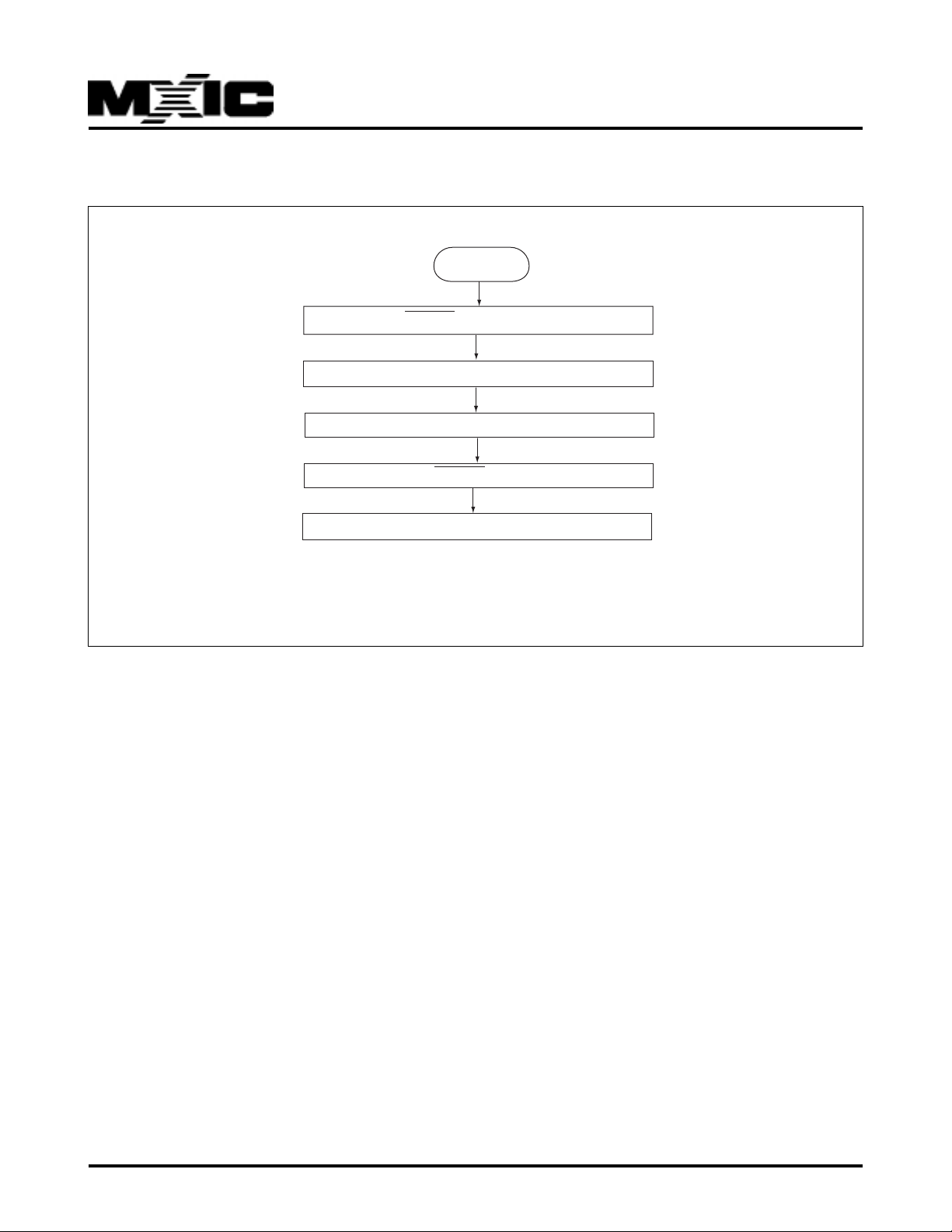
Figure 27. TEMPORAR Y SECT OR UNPROTECT ALGORITHM
Start
RESET = VID (Note 1)
Perform Erase or Program Operation
Operation Completed
RESET = VIH
Temporary Sector Unprotect Completed(Note 2)
MX29LV004T/B
Note : 1. All protected sectors are temporary unprotected.
2. All previously protected sectors are protected again.
VID=11.5V~12.5V
P/N:PM0732
REV. 1.1, SEP. 19, 2001
47
Page 48
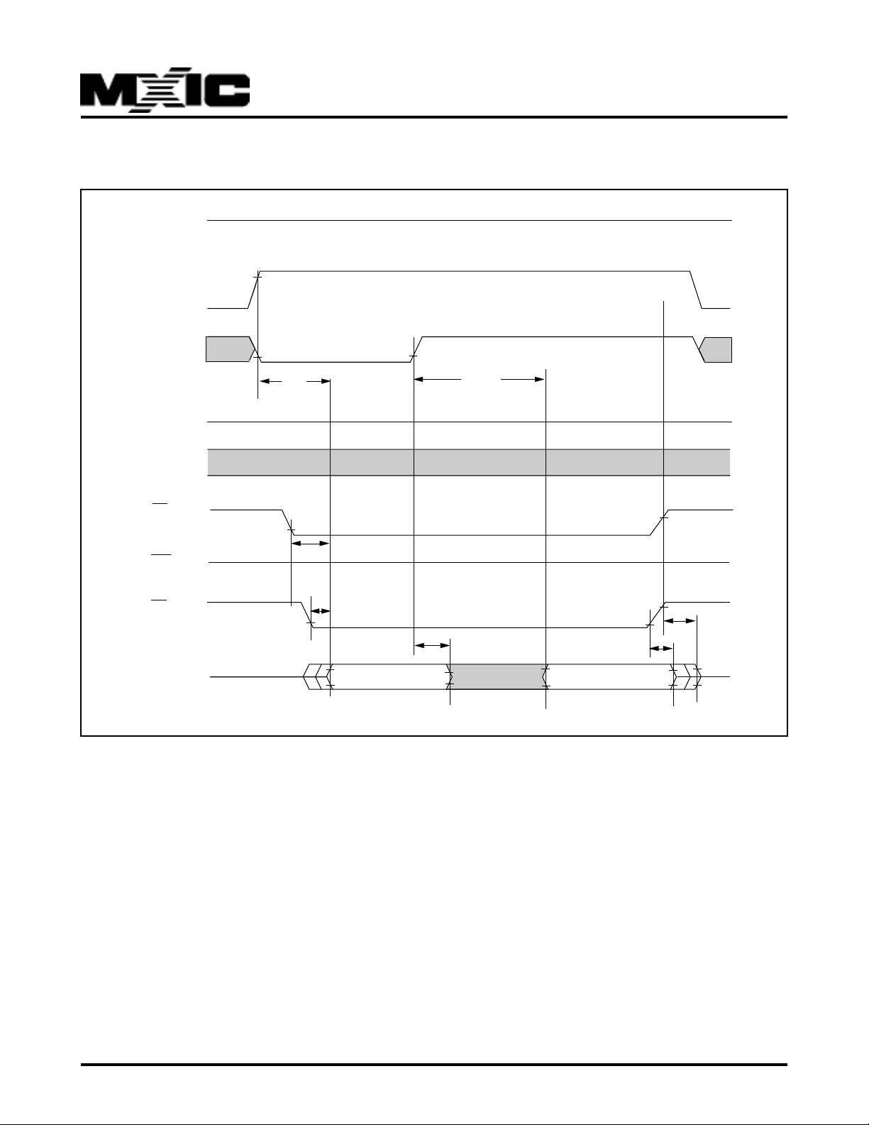
Figure 28. ID CODE READ TIMING WAVEFORM
MX29LV004T/B
VCC
ADD
A9
ADD
A0
A1
ADD
A2-A8
A10-A18
CE
WE
OE
VIH
VIL
VIH
VIL
VIH
VIL
VIH
VIL
VIH
VIL
VIH
VIL
3V
VID
VIH
VIL
tACC
tACC
tCE
tOE
tDF
DATA
Q0-Q7
VIH
VIL
DATA OUT
C2H
tOH
tOH
DATA OUT
B5H/B6H
P/N:PM0732
REV. 1.1, SEP. 19, 2001
48
Page 49
MX29LV004T/B
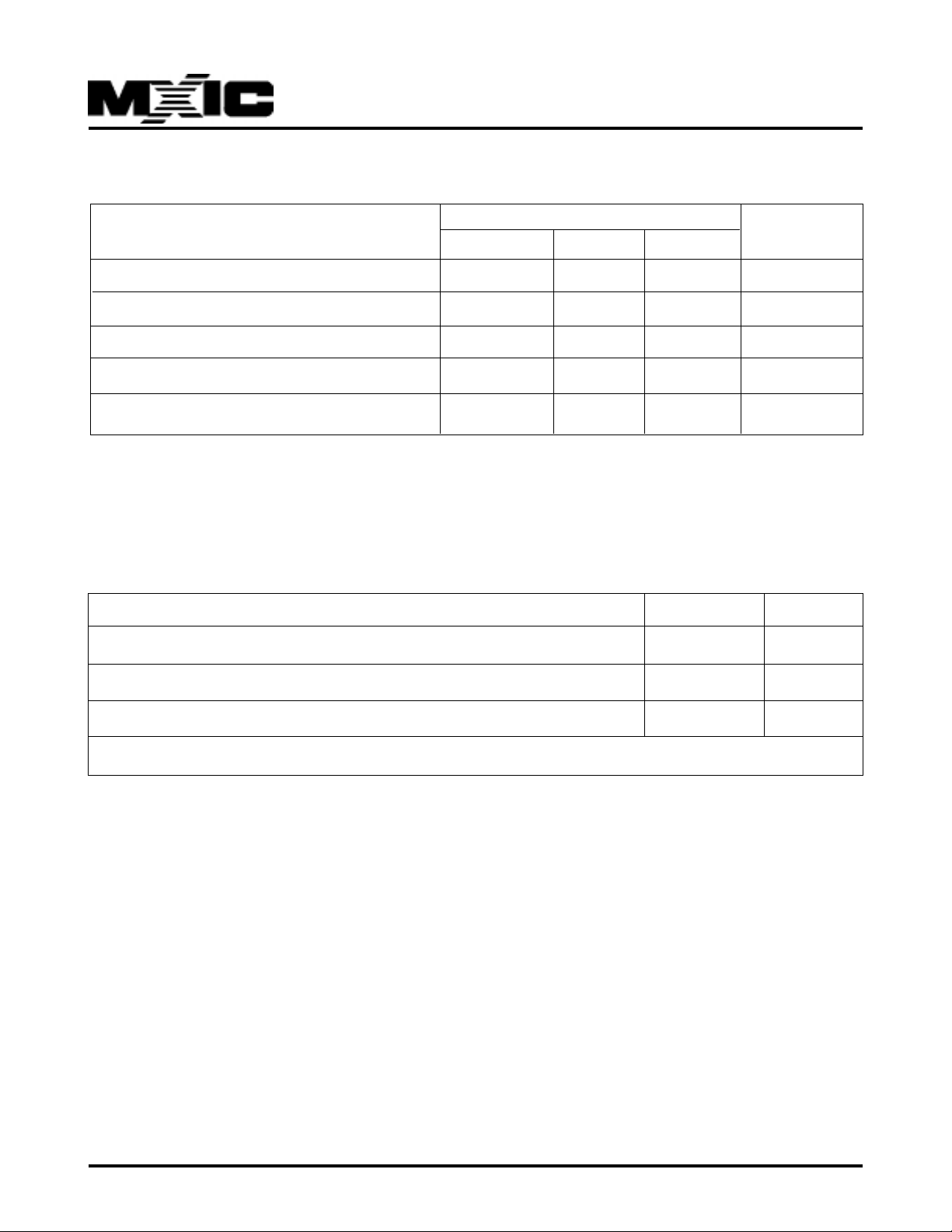
Table 15. ERASE AND PROGRAMMING PERFORMANCE(1)
LIMITS
PARAMETER MIN. TYP.(2) MAX.(3) UNITS
Sector Erase Time 0.7 15 sec
Chip Erase Time 11 s ec
Byte Programming Time 9 3 00 u s
Chip Programming Time 4.5 13.5 sec
Erase/Program Cycles 100,000 Cycles
Note: 1.Not 100% Tested, Excludes external system level o ver head.
2.Typical values measured at 25°C, 3V .
3.Maximum values measured at 25°C, 2.7V .
Table 16. LATCHUP CHARACTERISTICS
MIN. MAX.
Input Voltage with respect to GND on all pins except I/O pins -1.0V 12.5V
Input Voltage with respect to GND on all I/O pins -1.0V Vcc + 1.0V
Current -100mA +100mA
Includes all pins except Vcc. Test conditions: Vcc = 3.0V, one pin at a time.
P/N:PM0732
REV. 1.1, SEP. 19, 2001
49
Page 50

MX29LV004T/B
ORDERING INFORMATION
PLASTIC PACKAGE
P ART NO . ACCESS TIME OPERA TING CURRENT ST ANDBY CURRENT P A CKA GE
(ns) MAX.(mA) MAX.(uA)
MX29LV004TTC-55R 55 3 0 5 40 Pin TSOP
MX29LV004BTC-55R 55 3 0 5 40 Pin TSOP
MX29LV004TTC-70 70 3 0 5 40 Pin TSOP
MX29L V004BTC-70 70 3 0 5 40 Pin TSOP
MX29LV004TTC-90 90 3 0 5 40 Pin TSOP
MX29L V004BTC-90 90 3 0 5 40 Pin TSOP
MX29L V004TTI-70 70 30 5 40 Pin TSOP
MX29L V004BTI-70 70 30 5 40 Pin TSOP
MX29L V004TTI-90 90 30 5 40 Pin TSOP
MX29L V004BTI-90 90 30 5 40 Pin TSOP
MX29L V004TQC-55R 55 30 5 32 Pin PLCC
MX29L V004BQC-55R 55 30 5 32 Pin PLCC
MX29L V004TQC-70 70 30 5 32 Pin PLCC
MX29L V004BQC-70 70 3 0 5 32 Pin PLCC
MX29L V004TQC-90 70 30 5 32 Pin PLCC
MX29L V004BQC-90 70 3 0 5 32 Pin PLCC
MX29L V004TQI-70 70 3 0 5 32 Pin PLCC
MX29L V004BQI-70 70 30 5 32 Pin PLCC
MX29L V004TQI-90 70 3 0 5 32 Pin PLCC
MX29L V004BQI-90 70 30 5 32 Pin PLCC
P/N:PM0732
REV. 1.1, SEP. 19, 2001
50
Page 51
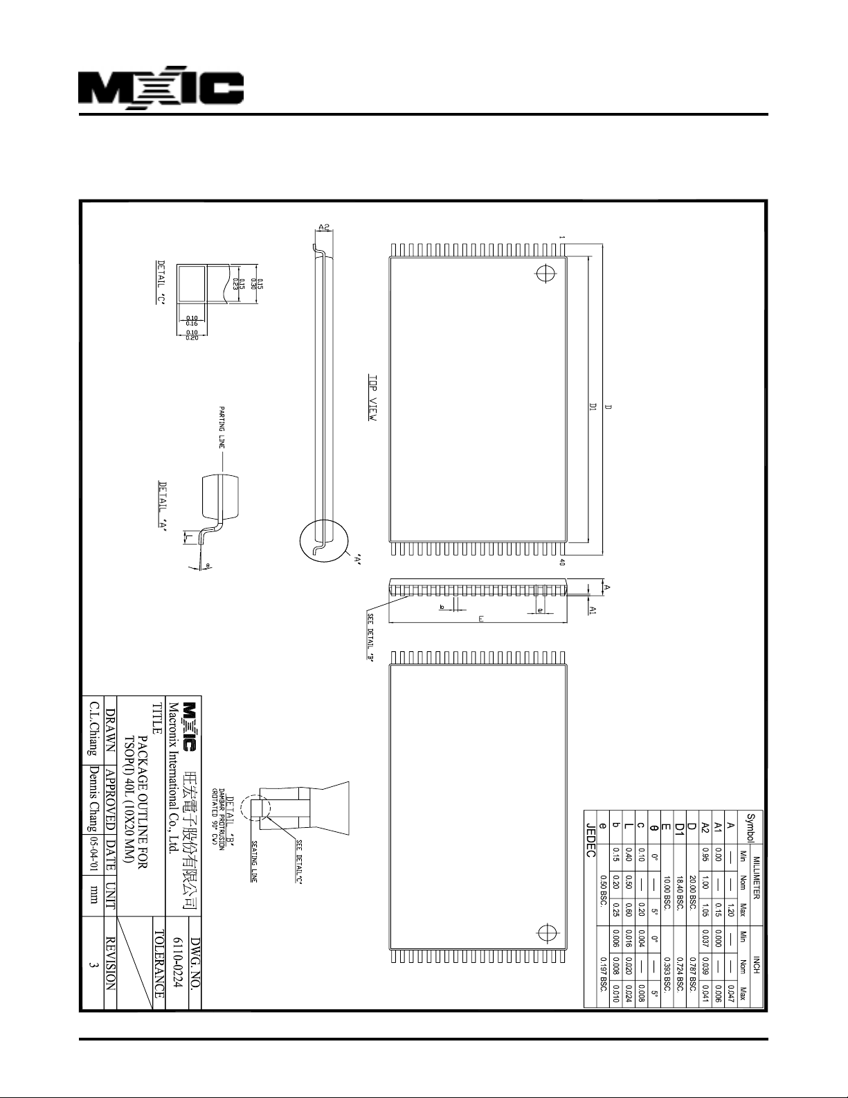
PACKAGE INFORMATION
40-PIN PLASTIC TSOP
MX29LV004T/B
P/N:PM0732
REV. 1.1, SEP. 19, 2001
51
Page 52
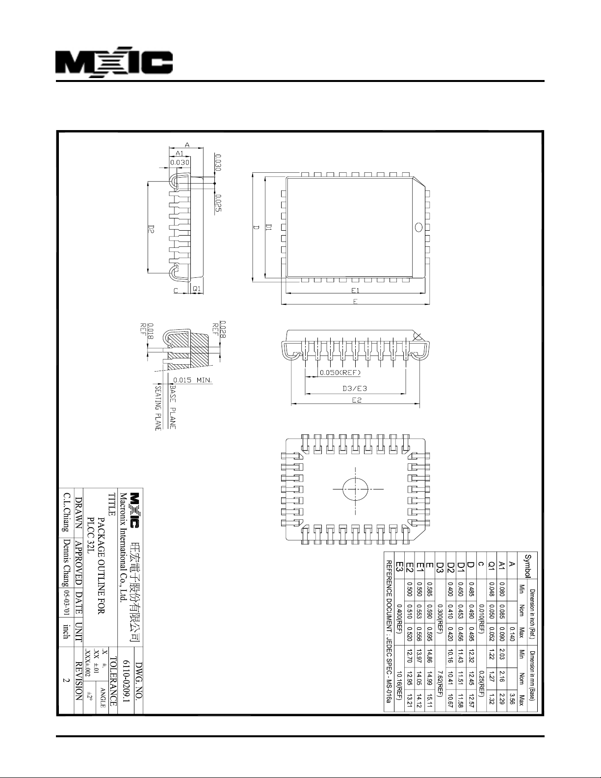
32-PIN PLCC
MX29LV004T/B
P/N:PM0732
REV. 1.1, SEP. 19, 2001
52
Page 53

MX29LV004T/B
REVISION HISTORY
Revision No. Description Page Date
1.0 Removed "Advance Information" heading P 1 JUL/26/2001
Added 32-PLCC package type P1,2,4,6,8,9,14
P19,23,43,48,50
Correct mis-typing P5,13,18,46
tBUSY was changed from 90us to 90ns P23
1.1 Correct mis-typing P10,19,34,35,38 SEP/19/2001
P39,40
Erase suspend spec was changed from 100us max. to 20us max.P13
The conditions of ICC4 was changed from CE;RESET=VCC±0.3VP19
to RESET=VSS±0.3V
Add typical spec for tWPP1 & tWPP2 P23
tBUSY spec was changed from 90ns min. to 90ns max. P23
Add sector protect (A9, OE control) waveform & flowchart P36,37
P/N:PM0732
REV. 1.1, SEP. 19, 2001
53
Page 54

MX29LV004T/B
MACRONIX INTERNATIONAL CO., LTD.
HEADQUARTERS:
TEL:+886-3-578-6688
FAX:+886-3-563-2888
EUROPE OFFICE:
TEL:+32-2-456-8020
FAX:+32-2-456-8021
JAPAN OFFICE:
TEL:+81-44-246-9100
FAX:+81-44-246-9105
SINGAPORE OFFICE:
TEL:+65-348-8385
FAX:+65-348-8096
TAIPEI OFFICE:
TEL:+886-2-2509-3300
FAX:+886-2-2509-2200
MACRONIX AMERICA, INC.
TEL:+1-408-453-8088
FAX:+1-408-453-8488
CHICAGO OFFICE:
TEL:+1-847-963-1900
FAX:+1-847-963-1909
http : //www.macronix.com
MACRONIX INTERNATIONAL CO., LTD. reserves the right to change product and specifications without notice.
52
 Loading...