

Page 1

FEATURES
ADVANCED INFORMATION
MX29L3211
32M-BIT [4M x 8/2M x 16] CMOS
SINGLE VOLTAGE PAGEMODE FLASH EEPROM
• 3.3V ± 10% write, erase and read
• Endurance: 10,000 cycles
• Fast random access time: 100ns/120ns
• Fast pagemode access time: 50ns
• Page access depth: 16 bytes/8 words
• Sector erase architecture
- 32 equal sectors of 64K word each
- Sector erase time: 200ms typical
• Auto Erase and Auto Program Algorithms
- Automatically erases any one of the sectors or the
whole chip with Erase Suspend capability
- Automatically programs and verifies data at specified
addresses
• Status Register feature for detection of program or
GENERAL DESCRIPTION
The MX29L3211 is a 32-mega bit pagemode Flash
memory organized as either 4M word x 8 or 2M byte x 16.
The MX29L3211 includes 32 sectors of 64K words.
MXIC's Flash memories offer the most cost-effective
and reliable read/write non-volatile random access
memory and fast page mode access. The MX29L3211
is packaged 44-pin SOP and 48-pin TSOP. It is designed
to be reprogrammed and erased in-system or in-standard
EPROM programmers.
The standard MX29L3211 offers access times as fast as
100ns,allowing operation of high-speed microprocessors
without wait. To eliminate bus contention, the MX29L3211
has separate chip enable CE, output enable (OE), and
write enable (WE) controls.
MXIC's Flash memories augment EPROM functionality
with in-circuit electrical erasure and programming. The
MX29L3211 uses a command register to manage this
functionality.
erase cycle completion
• Low VCC write inhibit is equal to or less than 1.8V
• Software data protection
• Page program operation
- Internal address and data latches for 256 bytes/128
words per page
- Page programming time: 5ms typical
• Low power dissipation
- 50mA active current
- 20uA standby current
• Two independently Protected sectors
• Industry standard surface mount packaging
- 44 pin SOP (500mil)
- 48 TSOP(I)
To allow for simple in-system reprogrammability, the
MX29L3211 does not require high input voltages for
programming. Three-volt-only commands determine
the operation of the device. Reading data out of the
device is similar to reading from an EPROM.
MXIC Flash technology reliably stores memory contents
even after 10,000 cycles. The MXIC's cell is designed
to optimize the erase and programming mechanisms. In
addition, the combination of advanced tunnel oxide
processing and low internal electric fields for erase and
programming operations produces reliable cycling. The
MX29L3211 uses a 3.3V ± 10% VCC supply to perform
the Auto Erase and Auto Program algorithms.
The highest degree of latch-up protection is achieved
with MXIC's proprietary non-epi process. Latch-up
protection is proved for stresses up to 100 milliamps on
address and data pin from -1V to VCC +1V.
P/N:PM0641
REV. 0.3, NOV. 06, 2001
1
Page 2
MX29L3211
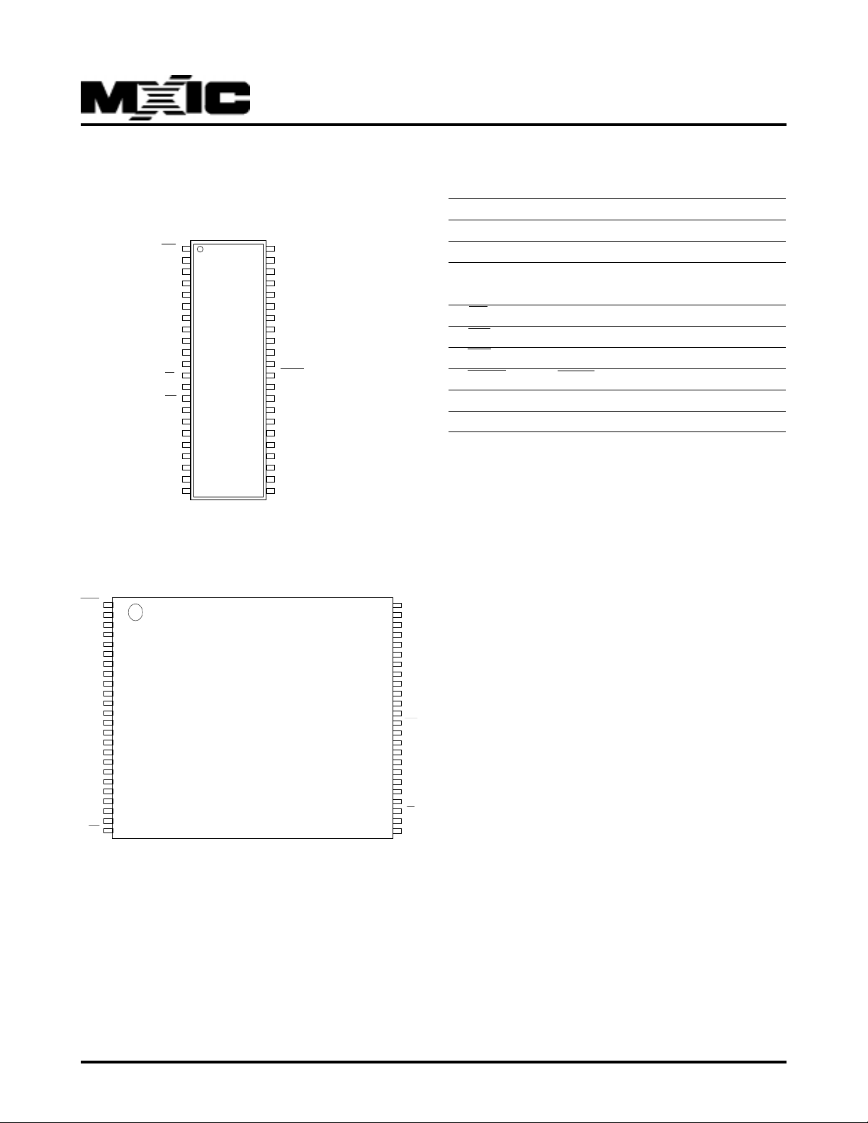
PIN CONFIGURATIONS
44 SOP(500mil)
WE
2
A18
3
A17
4
A7
5
A6
6
A5
7
A4
8
A3
9
A2
10
A1
11
A0
12
CE
13
GND
14
OE
15
Q0
16
Q8
17
Q1
18
Q9
19
Q2
20
Q10
21
Q3
22
Q11
48 TSOP (Normal Type)
44
43
42
41
40
39
38
37
36
35
34
33
32
MX29L3211
31
30
29
28
27
26
25
24
23
A20
A19
A8
A9
A10
A11
A12
A13
A14
A15
A16
BYTE
GND
Q15/A-1
Q7
Q14
Q6
Q13
Q5
Q12
Q4
VCC
PIN DESCRIPTION
SYMBOL PIN NAME
A0 - A20 Address Inputs
Q0 - Q14 Data Input/Output
Q15/A-1 Q15(Word mode)/LSB Address (Byte
mode)
CE Chip Enable Input
OE Output Enable Input
WE Write Enable Input
BYTE BYTE/Word Mode Selection
VCC Power Supply
GND Ground Pin
BYTE
A16
A15
A14
A13
A12
A11
A10
A9
A8
A19
GND
A20
A18
A17
A7
A6
A5
A4
A3
A2
A1
A0
CE
1
2
3
4
5
6
7
8
9
10
11
12
13
14
15
16
17
18
19
20
21
22
23
24
MX29L3211
(Normal T ype)
48
GND
47
GND
46
Q15/A-1
45
Q7
44
Q14
43
Q6
42
Q13
41
Q5
40
Q12
39
Q4
38
VCC
37
VCC
36
WE
35
Q11
34
Q3
33
Q10
32
Q2
31
Q9
30
Q1
29
Q8
28
Q0
27
OE
26
GND
25
GND
P/N:PM0641
REV. 0.3, NOV. 06, 2001
2
Page 3
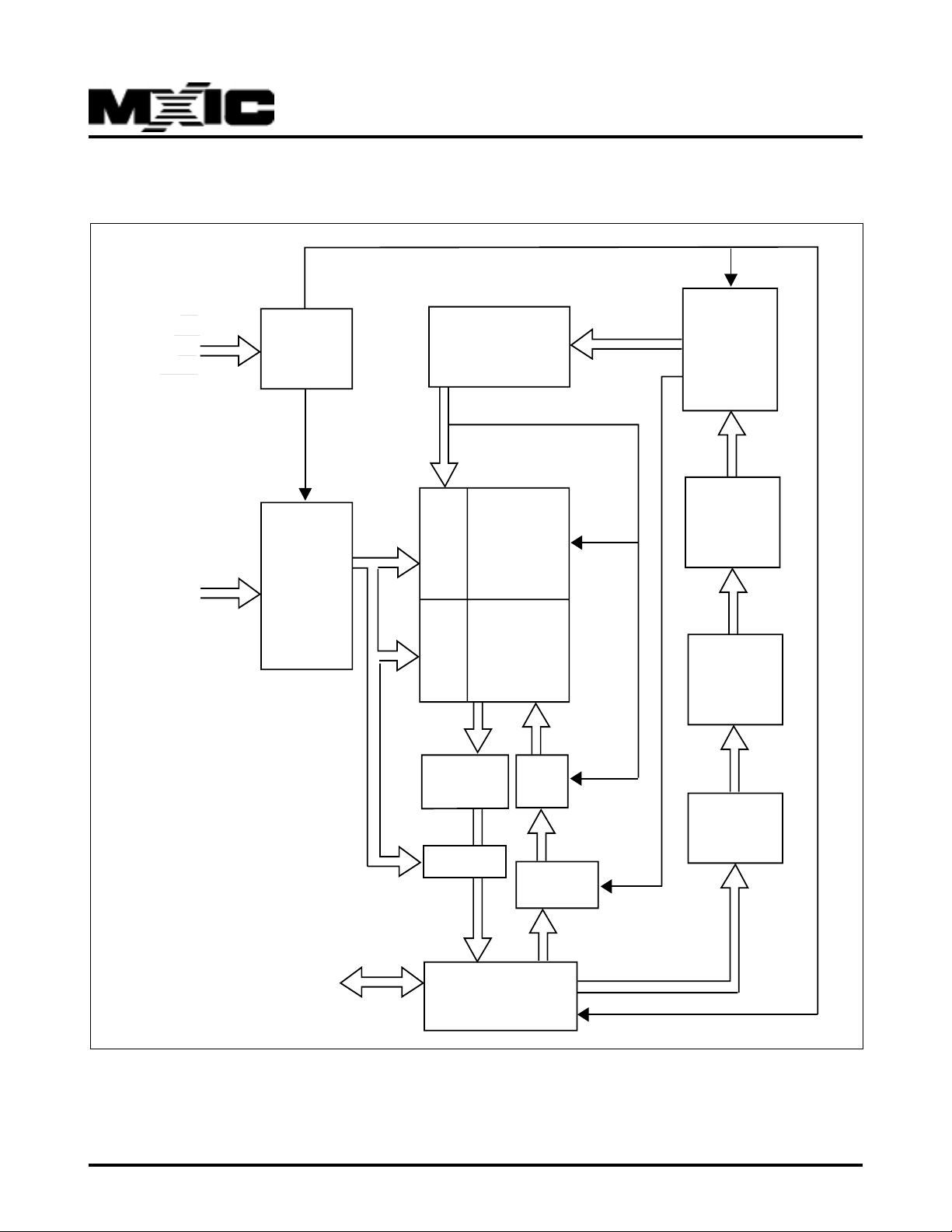
BLOCK DIAGRAM
CE
WE
OE
BYTE
CONTROL
INPUT
LOGIC
PROGRAM/ERASE
HIGH VOLT A GE
MX29L3211
WRITE
STATE
MACHINE
(WSM)
Q15/A-1
A0-A20
ADDRESS
LA TCH
AND
BUFFER
X-DECODER
MX29L3211
FLASH
ARRA Y
Y-DECODER
Y-PASS GATE
SENSE
AMPLIFIER
Y-select
COMMAND
INTERF ACE
REGISTER
(CIR)
ARRAY
SOURCE
HV
COMMAND
DATA
DECODER
PGM
DATA
HV
COMMAND
DATA LATCH
PROGRAM
DATA LATCH
P/N:PM0641
Q0-Q15/A-1
I/O BUFFER
REV. 0.3, NOV. 06, 2001
3
Page 4

MX29L3211
Table1.PIN DESCRIPTIONS
SYMBOL TYPE NAME AND FUNCTION
A0 - A20 INPUT ADDRESS INPUTS: for memory addresses. Addresses are internally
latched during a write cycle.
Q0 - Q7 INPUT/OUTPUT LOW-BYTE DATA BUS: Input data and commands during Command Interface
Register(CIR) write cycles. Outputs array,status and identifier data in the
appropriate read mode. Floated when the chip is de-selected or the outputs
are disabled.
Q8 - Q14 INPUT/OUTPUT HIGH-BYTE DATA BUS: Inputs data during x 16 Data-Write operations.
Outputs array, identifier data in the appropriate read mode; not used for status
register reads. Floated when the chip is de-selected or the outputs are
disabled
Q15/A -1 INPUT/OUTPUT Selects between high-byte data INPUT/OUTPUT(BYTE = HIGH) and LSB
ADDRESS(BYTE = LOW)
CE INPUT CHIP ENABLE INPUTS: Activate the device's control logic, Input buffers,
decoders and sense amplifiers. With CE high, the device is deselected and
power consumption reduces to Standby level upon completion of any current
program or erase operations. CE must be low to select the device.
OE INPUT OUTPUT ENABLES: Gates the device's data through the output buffers
during a read cycle OE is active low.
WE INPUT WRITE ENABLE: Controls writes to the Command Interface Register(CIR).
WE is active low.
BYTE INPUT BYTE ENABLE: BYTE Low places device in x8 mode. All data is then input
or output on Q0-7 and Q8-14 float. AddressQ15/A-1 selects between the high
and low byte. BYTE high places the device in x16 mode, and turns off the Q15/
A-1 input buffer. Address A0, then becomes the lowest order address.
VCC DEVICE POWER SUPPLY(3.3V ± 10%)
GND GROUND
P/N:PM0641
REV. 0.3, NOV. 06, 2001
4
Page 5
MX29L3211
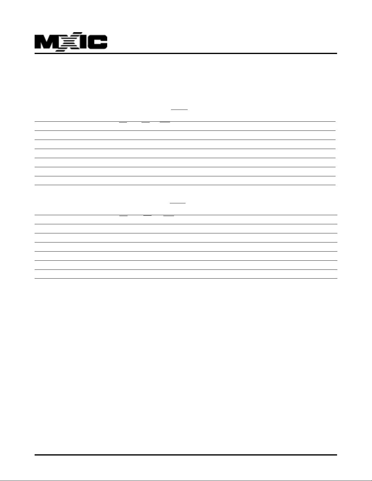
BUS OPERATION
Flash memory reads, erases and writes in-system via the local CPU . All bus cycles to or from the flash memory
conform to standard microprocessor bus cycles.
Table 2.1 Bus Operations for Word-Wide Mode (BYTE = VIH)
Mode Notes CE OE WE A0 A1 A9 Q0-Q7 Q8-Q14 Q15/A-1
Read 1 VIL VIL VIH X X X DOUT DOUT DOUT
Output Disable 1 VIL VIH VIH X X X High Z High Z HighZ
Standby 1 VIH X X X X X High Z HIgh Z HighZ
Manufacturer ID 2,4 VIL VIL VIH VIL VIL VID C2H 00H 0B
Device ID 2,4 VIL VIL VIH VIH VIL VID F9H 00H 0B
Write 1,3 VIL VIH VIL X X X DIN DIN DIN
Table2.2 Bus Operations for BYTE-Wide Mode (BYTE = VIL)
Mode Notes CE OE WE A0 A1 A9 Q0-Q7 Q8-Q14 Q15/A-1
Read 1 VIL VIL VIH X X X DOUT HighZ VIL/VIH
Output Disable 1 VIL VIH VIH X X X High Z High Z X
Standby 1 VIH X X X X X High Z HIgh Z X
Manufacturer ID 2,4 VIL VIL VIH VIL VIL VID C2H High Z VIL
Device ID 2,4 VIL VIL VIH VIH VIL VID F9H High Z VIL
Write 1,3 VIL VIH VIL X X X DIN High Z VIL/VIH
NOTES :
1. X can be VIH or VIL for address or control pins.
2. A0 and A1 at VIL provide manufacturer ID codes. A0 at VIH and A1 at VIL provide device ID codes. A0 at VIL, A1 at VIH and
with appropriate sector addresses provide Sector Protect Code.(Refer to Table 4)
3. Commands for different Erase operations, Data program operations or Sector Protect operations can only be successfully
completed through proper command sequence.
4. VID = 11.5V- 12.5V.
P/N:PM0641
5
REV. 0.3, NOV. 06, 2001
Page 6
WRITE OPERATIONS
MX29L3211
Commands are written to the COMMAND INTERFACE
REGISTER (CIR) using standard microprocessor write
timings. The CIR serves as the interface between the
microprocessor and the internal chip operation. The
CIR can decipher Read Array, Read Silicon ID, Erase
and Program command. In the event of a read command,
the CIR simply points the read path at either the array or
CIR will only respond to status reads. During a sector/
chip erase cycle, the CIR will respond to status reads
and erase suspend. After the write state machine has
completed its task, it will allow the CIR to respond to its
full command set. The CIR stays at read status register
mode until the microprocessor issues another valid
command sequence.
the silicon ID, depending on the specific read command
given. For a program or erase cycle, the CIR informs the
write state machine that a program or erase has been
requested. During a program cycle, the write state
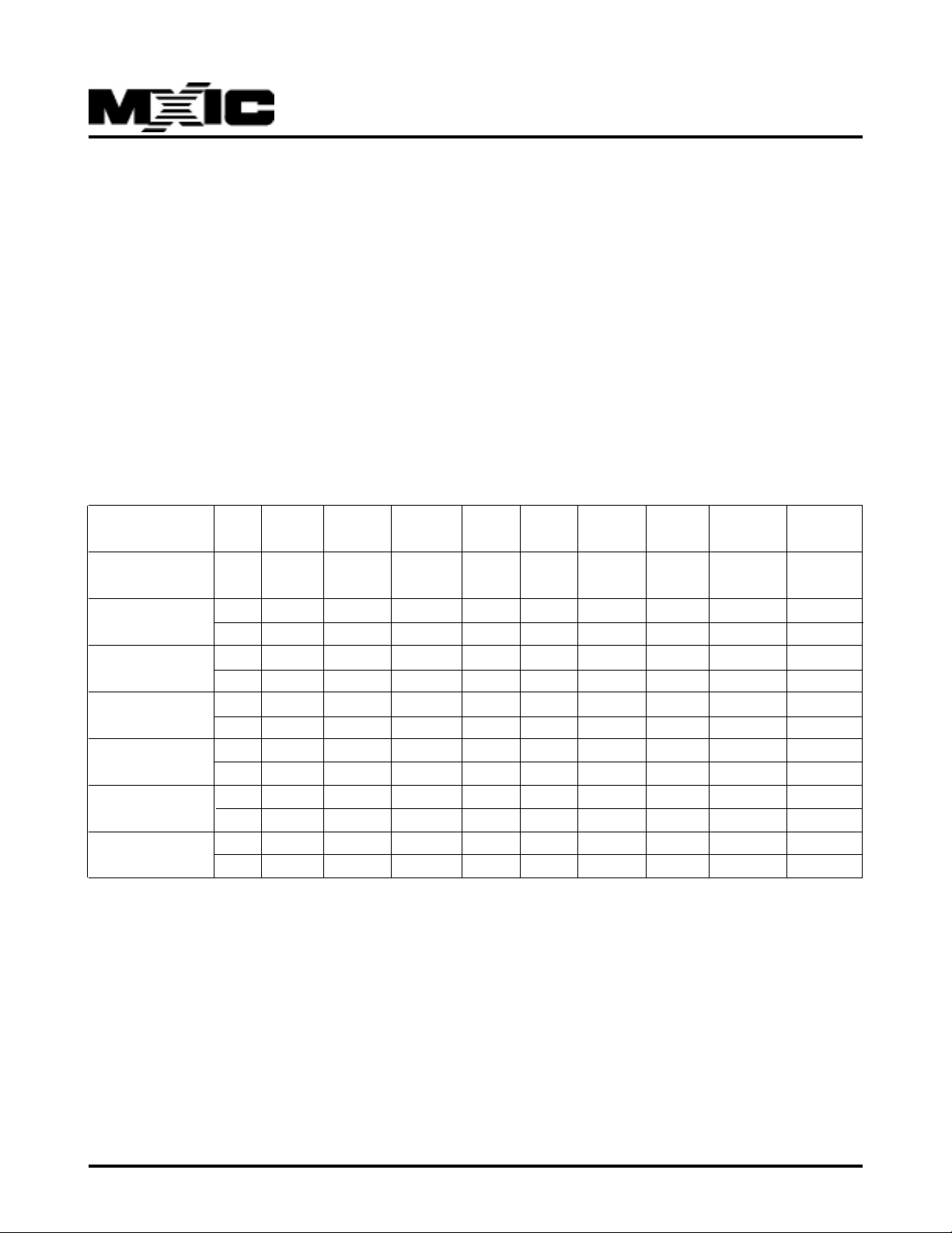
Device operations are selected by writing commands
into the CIR. Table 3 below defines 32 Mbit flash family
command.
machine will control the program sequences and the
TABLE 3. COMMAND DEFINITIONS
Command Read/ Silicon Page/Byte Chip Sector Erase Erase Read Clear
Sequence Reset ID Read Program Erase Erase Suspend Resume Status Reg. Status Reg.
Bus Write 4 4 4 6 6 3 3 4 3
Cycles Req'd
First Bus Addr 5555H 5555H 5555H 5555H 5555H 5555H 5555H 5555H 5555H
Write Cycle Data AAH AAH AAH AAH AAH AAH AAH AAH AAH
Second Bus Addr 2AAAH 2AAAH 2AAAH 2AAAH 2AAAH 2AAAH 2AAAH 2AAAH 2AAAH
Write Cycle Data 55H 55H 55H 55H 55H 55H 55H 55H 55H
Third Bus Addr 5555H 5555H 5555H 5555H 5555H 5555H 5555H 5555H 5555H
Write Cycle Data F0H 90H A0H 80H 80H B0H D0H 70H 50H
Fourth Bus Addr RA 00H/01H PA 5555H 5555H X
Read/Write Cycle Data RD C2H/F9H PD AAH AAH SRD
Fifth Bus Addr 2AAAH 2AAAH
Write Cycle Data 55H 55H
Sixth Bus Addr 5555H SA
Write Cycle Data 10H 30H
P/N:PM0641
REV. 0.3, NOV. 06, 2001
6
Page 7
TABLE 3. COMMAND DEFINITIONS
Command Sector Sector Verify Sector Abort
Sequence Protection Unprotect Protect
Bus Write 6 6 4 3
Cycles Req'd
First Bus Addr 5555H 5555H 5555H 5555H
Write Cycle Data AAH AAH AAH AAH
Second Bus Addr 2AAAH 2AAAH 2AAAH 2AAAH
Write Cycle Data 55H 55H 55H 55H
Third Bus Addr 5555H 5555H 5555H 5555H
Write Cycle Data 60H 60H 90H E0H
Fourth Bus Addr 5555H 5555H *
Read/Write Cycle Data AAH A AH C2H*
Fifth Bus Addr 2AAAH 2AAAH
Write Cycle Data 55H 55H
Sixth Bus Addr SA** SA**
Write Cycle Data 20H 40H
MX29L3211
Notes:
1. Address bit A15 -- A20 = X = Don't care for all address commands except for Program Address(PA) and Sector Address(SA).
5555H and 2AAAH address command codes stand for Hex number starting from A0 to A14.
2. Bus operations are defined in Table 2.
3. RA = Address of the memory location to be read.
PA = Address of the memory location to be programmed. Addresses are latched on the falling edge of the WE pulse.
SA = Address of the sector to be erased. The combination of A16 -- A20 will uniquely select any sector.
4. RD = Data read from location RA during read operation.
PD = Data to be programmed at location PA. Data is latched on the rising edge of WE.
SRD = Data read from status register.
* Refer to Table 4, Figure 12.
** Only the top and the bottom sectors have protect- bit feature. SA = (A20,A19,A18,A17,A16) = 00000B or 11111B is valid.
P/N:PM0641
REV. 0.3, NOV. 06, 2001
7
Page 8
DEVICE OPERATION
SILICON ID READ
The Silicon ID Read mode allows the reading out of a
binary code from the device and will identify its
manufacturer and type. This mode is intended for use
by programming equipment for the purpose of
automatically matching the device to be programmed
with its corresponding programming algorithm. This
mode is functional over the entire temperature range of
the device.
To activate this mode, the programming equipment
must force VID (11.5V~12.5V) on address pin A9. Two
identifier bytes may then be sequenced from the device
outputs by toggling address A0 from VIL to VIH. All
addresses are don't cares except A0 and A1.
MX29L3211
The manufacturer and device codes may also be read
via the command register, for instances when the
MX29L3211 is erased or programmed in a system
without access to high voltage on the A9 pin. The
command sequence is illustrated in Table 3.
During the "Silicon ID Read" Mode, manufacturer's code
(MXIC=C2H) can be read out by setting A0=VIL and
device identifier (MX29L3211=F9H) can be read out by
setting A0=VIH.
To terminate the operation, it is necessary to write the
read/reset command sequence into the CIR.
Table 4. MX29L3211 Silion ID Codes and Verify Sector Protect Code
Type A
Manufacturer Code X X X X X VI L VIL C2H* 1 1 0 0 0 0 1 0
MX29L3211 Device Code X X X X X VIL VIH F9H* 1 1 1 1 1 0 0 1
Verify Sector Protect Sector Address*** VIH VIL C2H** 1 1 0 0 0 0 1 0
* MX29L3211 Manufacturer Code = C2H, Device Code = F9H when BYTE = VIL
MX29L3211 Manufacturer Code = 00C2H, Device Code = 00F9H when BYTE = VIH
** Outputs C2H at protected sector address, 00H at unprotected scetor address.
***Only the top and the bottom sectors have protect-bit feature. Sector address = (A20, A19, A18,A17,A16) = 00000B or 11111B
A19A18A17A16A1A0Code(HEX) Q7Q6Q5Q4Q3Q
20
Q1Q
2
0
P/N:PM0641
REV. 0.3, NOV. 06, 2001
8
Page 9

MX29L3211
READ/RESET COMMAND
The read or reset operation is initiated by writing the
read/reset command sequence into the command
register. Microprocessor read cycles retrieve array data
from the memory. The device remains enabled for reads
until the CIR contents are altered by a valid command
sequence.
The device will automatically power-up in the read/reset
state. In this case, a command sequence is not required
for "read operation". Standard microprocessor read
cycles will retrieve array data. This default value ensures
that no spurious alteration of the memory content occurs
during the power transition. Refer to the AC Read
Characteristics and Waveforms for the specific timing
parameters.
The MX29L3211 is accessed like an EPROM. When CE
and OE are low and WE is high the data stored at the
memory location determined by the address pins is
asserted on the outputs. The outputs are put in the high
impedance state whenever CE or OE is high. This dual
line control gives designers flexibility in preventing bus
contention.
Note that the read/reset command is not valid when
program or erase is in progress.
After three-cycle command sequence is given, a
byte(word) load is performed by applying a low pulse on
the WE or CE input with CE or WE low (respectively) and
OE high. The address is latched on the falling edge of
CE or WE, whichever occurs last. The data is latched by
the first rising edge of CE or WE. Maximum of 128 words
of data may be loaded into each page by the same
procedure as outlined in the page program section
below.
BYTE-WIDE LOAD/WORD-WIDE LOAD
BYTE(word) loads are used to enter the 128 words(256
bytes) of a page to be programmed or the software
codes for data protection. A byte(word load) is performed
by applying a low pulse on the WE or CE input with CE
or WE low (respectively) and OE high. The address is
latched on the falling edge of CE or WE, whichever
occurs last. The data is latched by the first rising edge
of CE or WE.
Either word-wide load or byte-wide load is
determined(BYTE = VIL or VIH is latched) on the falling
edge of the WE (or CE) during the 3rd command write
cycle.
PROGRAM
PAGE READ
The MX29L3211 offers "fast page mode read" function.
The users can take the access time advantage if keeping
CE, OE at low and the same page address (A3~A20
unchanged). Please refer to Figure 5-2 for detailed
timing waveform. The system performance could be
enhanced by initiating 1 normal read and 7 fast page
reads(for word mode A0~A2) or 15 fast page reads(for
byte mode altering A-1~A2).
PAGE PROGRAM
To initiate Page Program mode, a three-cycle command
sequence is required. There are two "unlock" write
cycles. These are followed by writing the page program
command-A0H.
Any attempt to write to the device without the three-cycle
command sequence will not start the internal Write State
Machine(WSM), no data will be written to the device.
P/N:PM0641
Any page to be programmed should have the page in the
erased state first, i.e. performing sector erase is
suggested before page programming can be performed.
The device is programmed on a page basis. If a
byte(word) of data within a page is to be changed, data
for the entire page can be loaded into the device. Any
byte(word) that is not loaded during the programming of
its page will be still in the erased state (i.e. FFH). Once
the bytes of a page are loaded into the device, they are
simultaneously programmed during the internal
programming period. After the first data byte (word) has
been loaded into the device, successive byte(word) are
entered in the same manner. Each new byte(word) to
be programmed must have its high to low transition on
WE (or CE) within 30us of the low to high transition of WE
(or CE) of the preceding byte(word). A7 to A20 specify
the page address, i.e., the device is page-aligned on 128
word(256 byte)boundary. The page address must be
valid during each high to low transition of WE or CE. A1 to A6 specify the byte address within the page, A0 to
REV. 0.3, NOV. 06, 2001
9
Page 10

MX29L3211
A6 specify the word address withih the page. The byte
(word) may be loaded in any order; sequential loading is
not required. If a high to low transition of CE or WE is not
detected whithin 100us of the last low to high transition,
the load period will end and the internal programming
period will start. The Auto page program terminates
when status on Q7 is '1' at which time the device stays
at read status register mode until the CIR contents are
altered by a valid command sequence.(Refer to table
3,6 and Figure 1,7,8)
CHIP ERASE
Chip erase is a six-bus cycle operation. There are two
"unlock" write cycles. These are followed by writing the
"set-up" command-80H. Two more "unlock" write cycles
are then followed by the chip erase command-10H.
Chip erase does not require the user to program the
device prior to erase.
The automatic erase begins on the rising edge of the last
WE pulse in the command sequence and terminates
when the status on Q7 is "1" at which time the device
stays at read status register mode. The device remains
enabled for read status register mode until the CIR
contents are altered by a valid command sequence.(Refer
to table 3,6 and Figure 2,7,9)
Table 5. MX29L3211 Sector Address Table
(Word-Wide Mode)
A20 A19 A18 A1 7 A16 Address Range[A20,A0]
SA0 0 0 0 0 0 000000H--00FFFFH
SA1 0 0 0 0 1 010000H--01FFFFH
SA2 0 0 0 1 0 020000H--02FFFFH
SA3 0 0 0 1 1 030000H--03FFFFH
SA4 0 0 1 0 0 040000H--04FFFFH
... ... ... ... ... ................................
SA31 1 1 1 1 1 1F0000H--1FFFFFH
SECTOR ERASE
Sector erase is a six-bus cycle operation. There are two
"unlock" write cycles. These are followed by writing the
set-up command-80H. Two more "unlock" write cycles
are then followed by the sector erase command-30H.
The sector address is latched on the falling edge of WE,
while the command (data) is latched on the rising edge
of WE.
Sector erase does not require the user to program the
device prior to erase. The system is not required to
provide any controls or timings during these operations.
The automatic sector erase begins on the rising edge of
the last WE pulse in the command sequence and
terminates when the status on Q7 is "1" at which time the
device stays at read status register mode. The device
remains enabled for read status register mode until the
CIR contents are altered by a valid command
sequence.(Refer to table 3,6 and Figure 3,4,7,9)
ERASE SUSPEND
This command only has meaning while the the WSM is
executing SECTOR or CHIP erase operation, and
therefore will only be responded to during SECTOR or
CHIP erase operation. After this command has been
executed, the CIR will initiate the WSM to suspend erase
operations, and then return to Read Status Register
mode. The WSM will set the Q6 bit to a "1". Once the
WSM has reached the Suspend state,the WSM will set
the Q7 bit to a "1", At this time, WSM allows the CIR to
respond to the Read Array, Read Status Register, Abort
and Erase Resume commands only. In this mode, the
CIR will not resopnd to any other comands. The WSM
will continue to run, idling in the SUSPEND state,
regardless of the state of all input control pins.
ERASE RESUME
This command will cause the CIR to clear the suspend
state and set the Q6 to a '0', but only if an Erase Suspend
command was previously issued. Erase Resume will
not have any effect in all other conditions.
P/N:PM0641
REV. 0.3, NOV. 06, 2001
10
Page 11

MX29L3211
READ STATUS REGISTER
The MXIC's 32 Mbit flash family contains a status
register which may be read to determine when a program
or erase operation is complete, and whether that
operation completed successfully. The status register
may be read at any time by writing the Read Status
command to the CIR. After writing this command, all
subsequent read operations output data from the status
register until another valid command sequence is
written to the CIR. A Read Array command must be
written to the CIR to return to the Read Array mode.
The status register bits are output on Q3 - Q7(table 6)
whether the device is in the byte-wide (x8) or word-wide
(x16) mode for the MX29L3211. In the word-wide mode
the upper byte, Q(8:15) is set to 00H during a Read
Status command. In the byte-wide mode, Q(8:14) are
tri-stated and Q15/A-1 retains the low order address
function. Q0-Q1 is set to 0H in either x8 or x16 mode.
It should be noted that the contents of the status register
are latched on the falling edge of OE or CE whichever
occurs last in the read cycle. This prevents possible bus
errors which might occur if the contents of the status
register change while reading the status register. CE or
OE must be toggled with each subsequent status read,
or the completion of a program or erase operation will not
be evident.
CLEAR STATUS REGISTER
The Erase fail status bit (Q5) and Program fail status bit
(Q4) are set by the write state machine, and can only be
reset by the system software. These bits can indicate
various failure conditions(see Table 6). By allowing the
system software to control the resetting of these bits,
several operations may be performed (such as
cumulatively programming several pages or erasing
multiple blocks in squence). The status register may
then be read to determine if an error occurred during that
programming or erasure series. This adds flexibility to
the way the device may be programmed or erased.
Additionally, once the program(erase) fail bit happens,
the program (erase) operation can not be performed
further. The program(erase) fail bit must be reset by
system software before further page program or sector
(chip) erase are attempted. To clear the status register,
the Clear Status Register command is written to the CIR.
Then, any other command may be issued to the CIR.
Note again that before a read cycle can be initiated, a
Read command must be written to the CIR to specify
whether the read data is to come from the Array, Status
Register or Silicon ID.
The Status Register is the interface between the
microprocessor and the Write State Machine (WSM).
When the WSM is active, this register will indicate the
status of the WSM, and will also hold the bits indicating
whether or not the WSM was successful in performing
the desired operation. The WSM sets status bits four
through seven and clears bits six and seven, but cannot
clear status bits four and five. If Erase fail or Program fail
status bit is detected, the Status Register is not cleared
until the Clear Status Register command is written. The
MX29L3211 automatically outputs Status Register data
when read after Chip Erase, Sector Erase, Page Program
or Read Status Command write cycle. The default state
of the Status Register after powerup and return from
deep power-down mode is (Q7, Q6, Q5, Q4) = 1000B.
Q3 = 0 or 1 depends on sector-protect status, can not be
changed by Clear Status Register Command or Write
State Machine.
P/N:PM0641
REV. 0.3, NOV. 06, 2001
11
Page 12
MX29L3211
TABLE 6. MX29L3211 STATUS REGISTER
STATUS NOTES Q7 Q6 Q5 Q4 Q3
IN PROGRESS PROGRAM 1,2, 6 0 0 0 0 0/1
ERASE 1,3, 6 0 0 0 0 0/1
SUSPEND (NOT COMPLETE) 1,4, 6 0 1 0 0 0/1
(COMPLETE) 1 1 0 0 0/1
COMPLETE PROGRAM 1,2, 6 1 0 0 0 0/1
ERASE 1,3, 6 1 0 0 0 0/1
FAIL PROGRAM 1,5, 6 1 0 0 1 0/ 1
ERASE 1,5, 6 1 0 1 0 0/1
AFTER CLEARING STATUS REGISTER 6 1 0 0 0 0/1
NOTES:
1. Q7 : WRITE STATE MACHINE STATUS
1 = READY, 0 = BUSY
Q6 : ERASE SUSPEND STATUS
1 = SUSPEND, 0 = NO SUSPEND
Q5 : ERASE FAIL STATUS
1 = FAIL IN ERASE, 0 = SUCCESSFUL ERASE
Q4 : PROGRAM FAIL STATUS
1 = FAIL IN PROGRAM, 0 = SUCCESSFUL PROGRAM
Q3 : SECTOR-PROTECT STATUS
1 = SECTOR 0 OR/AND 15 PROTECTED
0 = NONE OF SECTOR PROTECTED
Q2 - 0 = RESERVED FOR FUTURE ENHANCEMENTS.
These bits are reserved for future use ; mask them out when polling the Status Register.
2. PROGRAM STATUS is for the status during Page Programming or Sector Unprotect mode.
3. ERASE STATUS is for the status during Sector/Chip Erase or Sector Protection mode.
4. SUSPEND STATUS is for both Sector and Chip Erase mode .
5. FAIL STATUS bit(Q4 or Q5) is provided during Page Program or Sector/Chip Erase modes respectively.
6. Q3 = 0 or1 depends on Sector-Protect Status.
P/N:PM0641
REV. 0.3, NOV. 06, 2001
12
Page 13

MX29L3211
SECTOR PROTECTION
The MX29L3211 features sector protection. This feature
will disable both program and erase operations in either
the top or the bottom sector (0 or 31). The sector
protection feature is enabled using system software by
the user(Refer to table 3). The device is shipped with
both sectors unprotected. Alternatively, MXIC may
protect sectors in the factory prior to shipping the device.
To activate this mode, a six-bus cycle operation is
required. There are two 'unlock' write cycles. These are
followed by writing the 'set-up' command. Two more
'unlock' write cycles are then followed by the Lock Sector
command - 20H. Sector address is latched on the falling
edge of CE or WE of the sixth cycle of the command
sequence. The automatic Lock operation begins on the
rising edge of the last WE pulse in the command sequence
and terminates when the Status on Q7 is '1' at which time
the device stays at the read status register mode.
The device remains enabled for read status register
mode until the CIR contents are altered by a valid
command sequence (Refer to table 3,6 and Figure
10,12 ).
VERIFY SECTOR PROTECT
To verify the Protect status of the Top and the Bottom
sector, operation is initiated by writing Silicon ID read
command into the command register. Following the
command write, a read cycle from address XXX0H
retrieves the Manufacturer code of C2H. A read cycle
from XXX1H returns the Device code F9H. A read cycle
from appropriate address returns information as to which
sectors are protected. To terminate the operation, it is
necessary to write the read/reset command sequence
into the CIR.
(Refer to table 3,4 and Figure 12)
A few retries are required if Protect status can not be
verified successfully after each operation.
SECTOR UNPROTECT
It is also possible to unprotect the sector , same as the
first five write command cycles in activating sector
protection mode followed by the Unprotect Sector
command -40H, the automatic Unprotect operation
begins on the rising edge of the last WE pulse in the
command sequence and terminates when the Status on
Q7 is '1' at which time the device stays at the read status
register mode. (Refer to table 3,6 and Figure 11,12)
The device remains enabled for read status register
mode until the CIR contents are altered by a valid
command sequence.
ABORT MODE
To activate Abort mode, a three-bus cycle operation is
required. The E0H command (Refer to table 3) only
stops Page program or Sector /Chip erase operation
currently in progress and puts the device in Abort mode.
So the program or erase operation will not be completed.
Since the data in some page/sectors is no longer valid
due to an incomplete program or erase operation, the
program fail (Q4) or erase fail (Q5)bit will be set.
A read array command MUST be written to bring the
device out of the abort state without incurring any wake
up latency. Note that once device is brought out, Clear
status register mode is required before a program or
erase operation can be executed.
DATA PROTECTION
The MX29L3211 is designed to offer protection against
accidental erasure or programming caused by spurious
system level signals that may exist during power
transitions. During power up the device automatically
resets the internal state machine in the Read Array mode.
Also, with its control register architecture, alteration of the
memory contents only occurs after successful completion
of specific multi-bus cycle command sequences.
P/N:PM0641
The device also incorporates several features to prevent
inadvertent write cycles resulting from VCC power-up
and power-down transitions or system noise.
REV. 0.3, NOV. 06, 2001
13
Page 14

LOW VCC WRITE INHIBIT
To avoid initiation of a write cycle during VCC power-up
and power-down, a write cycle is locked out for VCC less
than VLKO(typically 1.8V). If VCC < VLKO, the command
register is disabled and all internal program/erase circuits
are disabled. Under this condition the device will reset
to the read mode. Subsequent writes will be ignored until
the VCC level is greater than VLKO. It is the user's
responsibility to ensure that the control pins are logically
correct to prevent unintentional write when VCC is
above VLKO.
WRITE PULSE "GLITCH" PROTECTION
Noise pulses of less than 10ns (typical) on CE or WE will
not initiate a write cycle.
LOGICAL INHIBIT
MX29L3211
Writing is inhibited by holding any one of OE = VIL,CE =
VIH or WE = VIH. To initiate a write cycle CE and WE
must be a logical zero while OE is a logical one.
P/N:PM0641
REV. 0.3, NOV. 06, 2001
14
Page 15
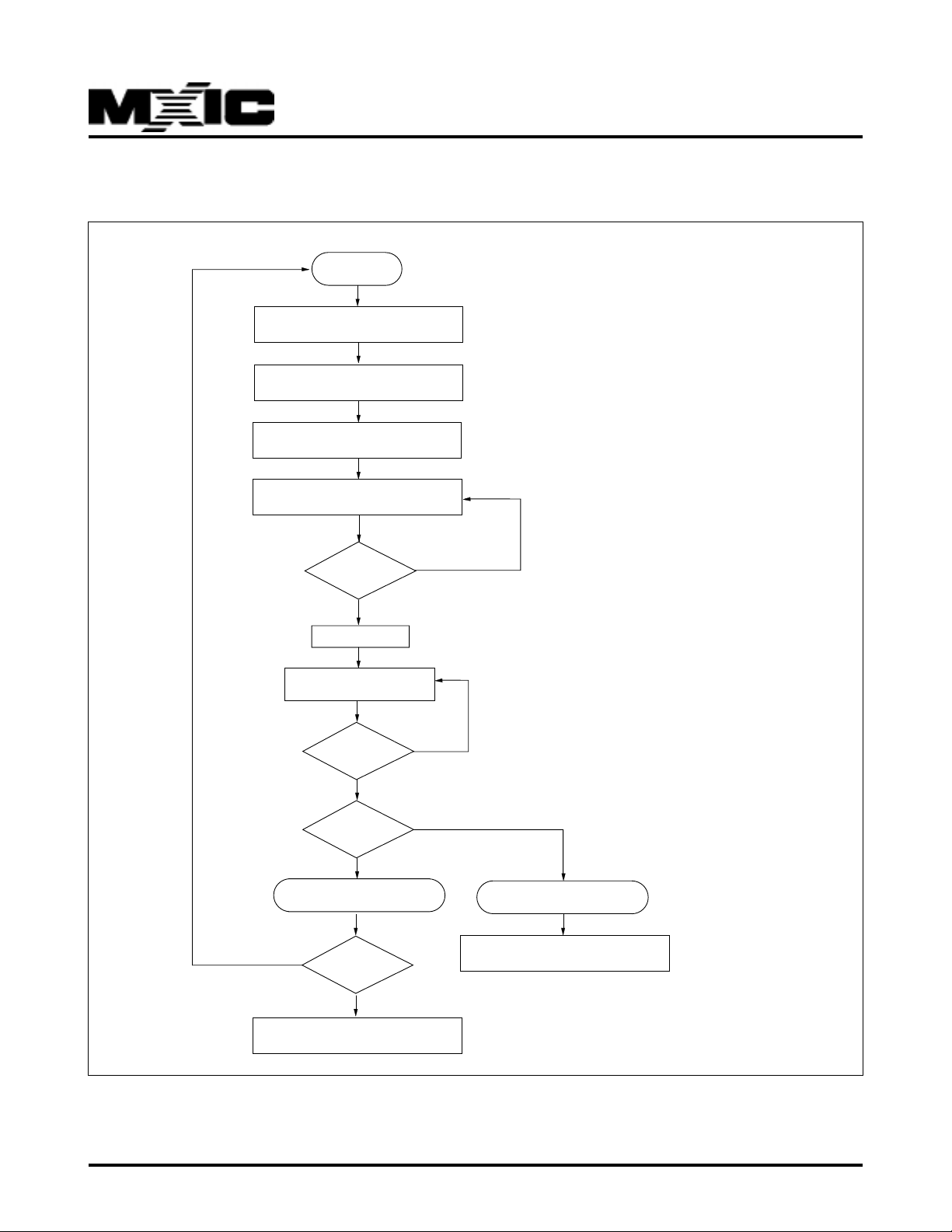
Figure 1. AUTOMATIC PAGE PROGRAM FLOW CHART
START
Write Data AAH Address 5555H
Write Data 55H Address 2AAAH
Write Data A0H Address 5555H
Write Program Data/Address
MX29L3211
Read Status Register
Page Program Completed
YES
Loading End?
YES
Wait 100us
SR7 = 1
?
YES
SR4 = 0
?
YES
Program
another page?
NO
NO
NO
NO
Program Error
To Continue Other Operations,
Do Clear S.R. Mode First
P/N:PM0641
Operation Done, Device Stays At Read S.R. Mode
Note : S.R. Stands for Status Register
REV. 0.3, NOV. 06, 2001
15
Page 16
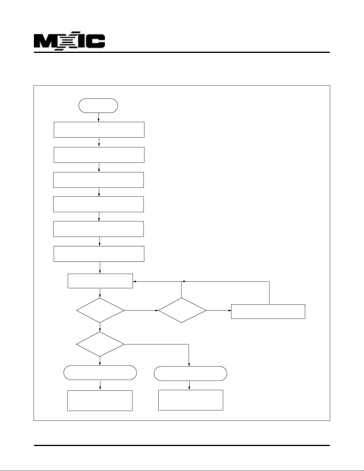
Figure 2. AUTOMATIC CHIP ERASE FLOW CHART
START
Write Data AAH Address 5555H
Write Data 55H Address 2AAAH
Write Data 80H Address 5555H
Write Data AAH Address 5555H
MX29L3211
Write Data 55H Address 2AAAH
Write Data 10H Address 5555H
Read Status Register
SR7 = 1
?
YES
SR5 = 0
?
YES
Chip Erase Completed
Operation Done,
Device Stays at
Read S.R. Mode
NO
NO
NO
To Execute
Suspend Mode ?
Erase Error
To Continue Other
Operations, Do Clear
S.R. Mode First
YES
Erase Suspend Flow (Figure 4.)
P/N:PM0641
REV. 0.3, NOV. 06, 2001
16
Page 17
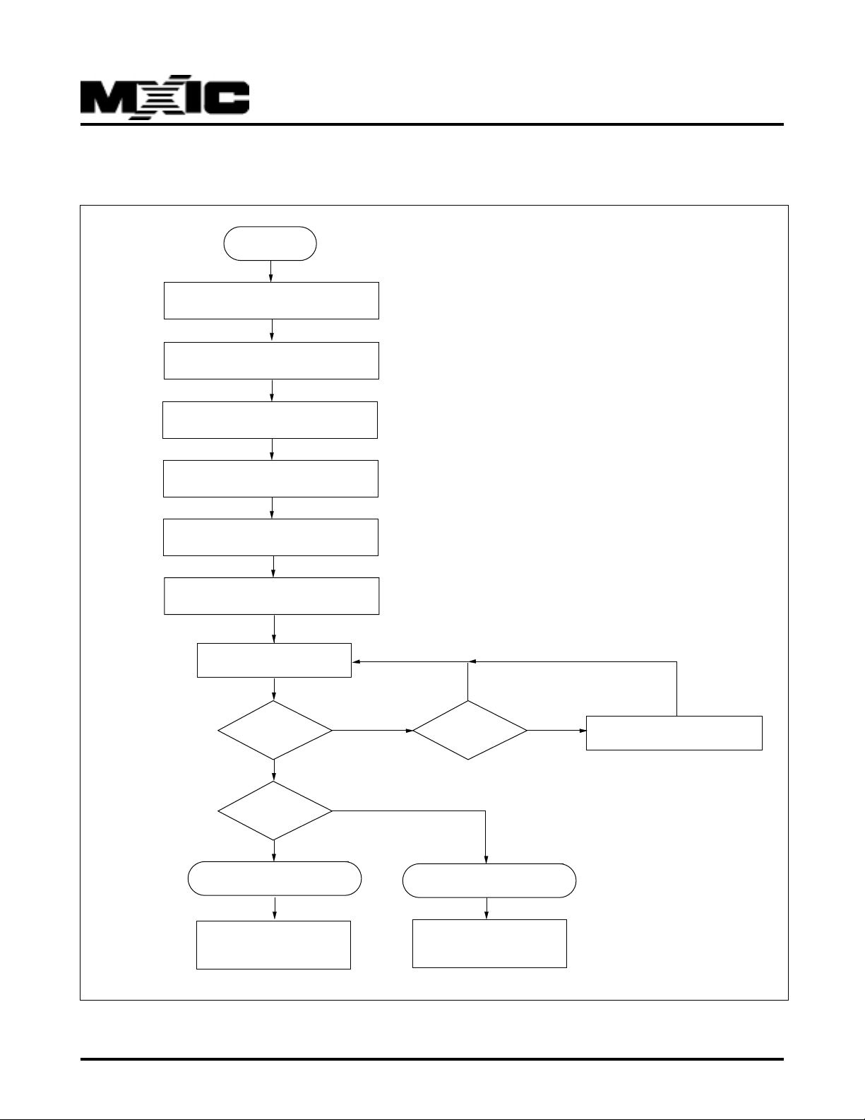
Figure 3. AUTOMATIC SECTOR ERASE FLOW CHART
START
Write Data AAH Address 5555H
Write Data 55H Address 2AAAH
Write Data 80H Address 5555H
Write Data AAH Address 5555H
MX29L3211
Write Data 55H Address 2AAAH
Write Data 30H Sector Address
Read Status Register
SR7 = 1
?
YES
SR5 = 0
?
YES
Sector Erase Completed
Operation Done,
Device Stays at
Read S.R. Mode
NO
NO
NO
To Execute
Suspend Erase ?
Erase Error
To Continue Other
Operations, Do Clear
S.R. Mode First
YES
Erase Suspend Flow (Figure 4.)
P/N:PM0641
REV. 0.3, NOV. 06, 2001
17
Page 18
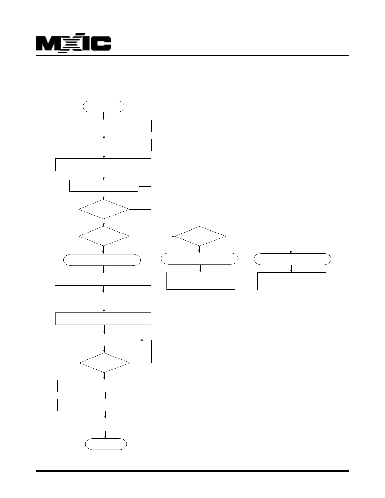
Figure 4. ERASE SUSPEND/ERASE RESUME FLOW CHART
START
Write Data AAH Address 5555H
Write Data 55H Address 2AAAH
Write Data B0H Address 5555H
Read Status Register
MX29L3211
SR7 = 1
?
YES
SR6 = 1
?
YES
Erase Suspend
Write Data AAH Address 5555H
Write Data 55H Address 2AAAH
Write Data F0H Address 5555H
Read Array
Reading End ?
YES
Write Data AAH Address 5555H
NO
NO
NO
SR5 = 0
?
YES
Erase has completed
Operation Done,
Device Stays at
Read S,R, Mode
NO
Erase Error
To Continue Other
Operations, Do Clear
S.R. Mode First
P/N:PM0641
Write Data 55H Address 2AAAH
Write Data D0H Address 5555H
Continue Erase
REV. 0.3, NOV. 06, 2001
18
Page 19
MX29L3211
ELECTRICAL SPECIFICATIONS
ABSOLUTE MAXIMUM RATINGS
RATING VALUE
Ambient Operating Temperature 0°C to 70°C
Storage Temperature -65°C to 125°C
Applied Input Voltage -0.5V to Vcc+0.5V
Applied Output Voltage -0.5V to Vcc+0.6V
VCC to Ground Potential -0.5V to 4V
A9 -0.5V to 12.5V
CAPACITANCE TA = 25
°°
°C, f = 1.0 MHz
°°
NOTICE:
Stresses greater than those listed under ABSOLUTE
MAXIMUM RATINGS may cause permanent damage to the
device. This is stress rating only and functional operational
sections of this specification is not implied. Exposure to
absolute maximum rating conditions for extended period may
affect reliability.
NOTICE:
Specifications contained within the following tables are subject
to change.
SYMBOL PARAMETER MIN. TYP. MAX. UNIT CONDITIONS
CIN Input Capacitance 14 pF VIN = 0V
COUT Output Capacitance 16 pF VOUT = 0V
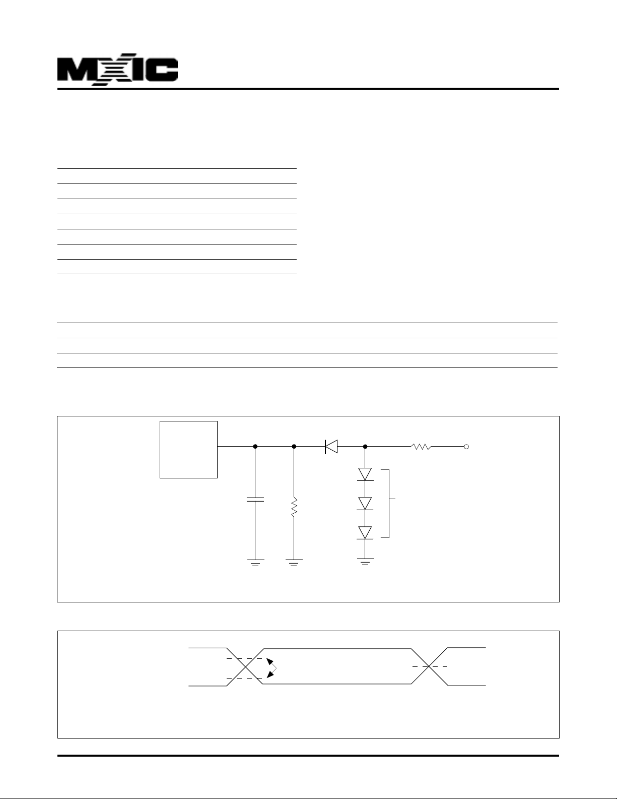
SWITCHING TEST CIRCUITS
DEVICE
UNDER
TEST
CL = 100 pF Including jig capacitance
SWITCHING TEST WAVEFORMS
2.4V
0.45V
INPUT
AC TESTING: Inputs are driven at 2.4V for a logic "1" and 0.45V for a logic "0".
Input pulse rise and fall times are < 5ns.
CL
2.0V
0.8V
6.2K ohm
TEST POINTS
2.7K ohm
DIODES = IN3064
OR EQUIVALENT
1.5V
OUTPUT
3.3V
P/N:PM0641
REV. 0.3, NOV. 06, 2001
19
Page 20

MX29L3211
5.1 DC CHARACTERISTICS Vcc = 3.3V
SYMBOL PARAMETER NOTES MIN. TYP. MAX. UNITS TEST CONDITIONS
IIL Input Load 1 ±1 uA VCC = VCC Max
Current VIN = VCC or GND
ILO Output Leakage 1 ±10 uA VCC = VCC Max
Current VIN = VCC or GND
ISB1 VCC Standby 1 20 50 uA VCC = VCC Max
Current(CMOS) CE = VCC± 0.2V
ISB2 VCC Standby 1 2 mA VCC = VCC Max
Current(TTL) CE = VIH
ICC1 VCC Read 1 50 80 mA VCC = VCC Max
Current f = 10MHz, IOUT = 0 mA
ICC2 VCC Erase 1,2 5 mA CE = VIH
Suspend Current Sector Erase Suspended
ICC3 VCC Program 1 30 60 mA Program in Progress
Current
ICC4 VCC Erase Current 1 30 60 mA Erase in Progress
VIL Input Low Voltage 3 -0.3 0.6 V
VIH Input High Voltage 4 0.7VCC VCC+0.3 V
VOL Output Low Voltage 0.45 V IOL = 2.1mA, Vcc = Vcc Min
VOH Output High Voltage 2.4 V IOH = -100uA, Vcc = Vcc Min
± ±
± 10%
± ±
NOTES:
1. All currents are in RMS unless otherwise noted. Typical values at VCC = 3.3V, T = 25°C. These currents are valid for all product
versions (package and speeds).
2. ICC2 is specified with the device de-selected. If the device is read while in erase suspend mode, current draw is the sum of
ICC2 and ICC1.
3. VIL min. = -1.0V for pulse width is equal to or less than 50ns.
VIL min. = -2.0V for pulse width is equal to or less than 20ns.
4. VIH max. = VCC + 1.5V for pulse width is equal to or less than 20ns. If VIH is over the specified maximum value, read operation
cannot be guaranteed.
P/N:PM0641
REV. 0.3, NOV. 06, 2001
20
Page 21
MX29L3211
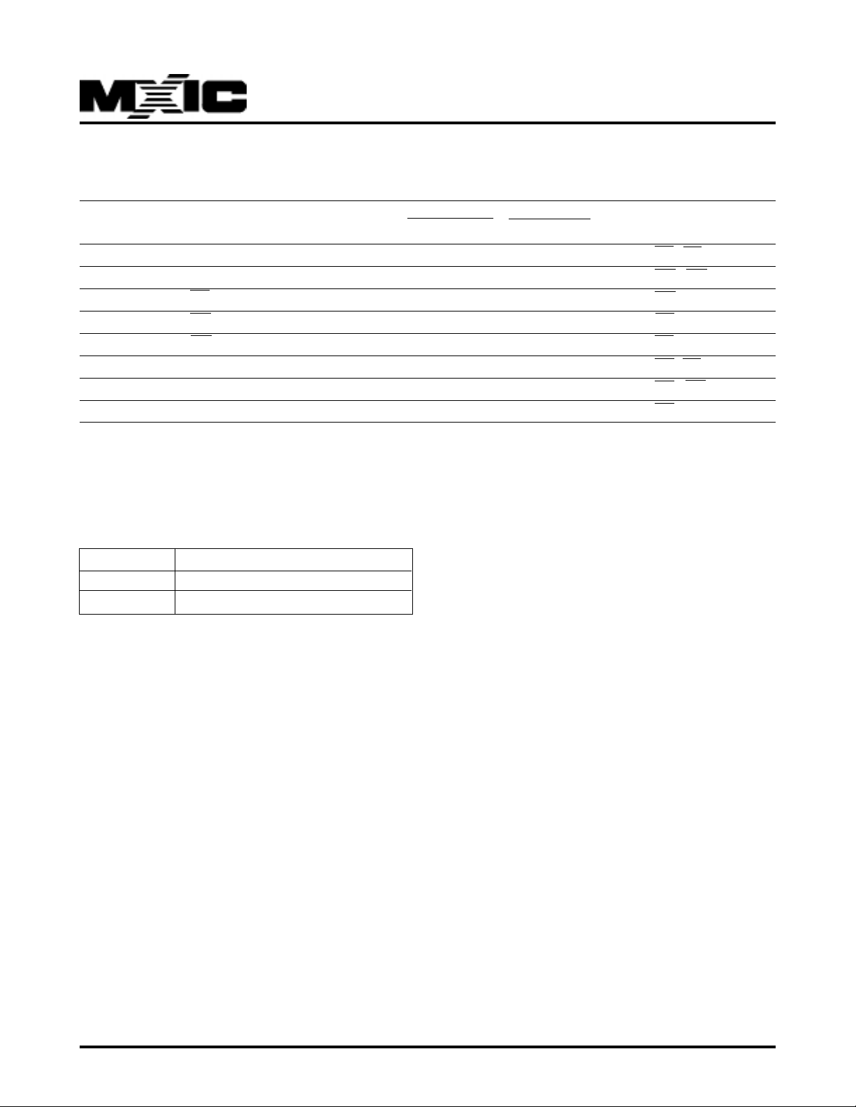
AC CHARACTERISTICS -- READ OPERATIONS
29L3211-10 29L3211-12
SYMBOL DESCRIPTIONS MIN. MAX. MIN. MAX. UNIT CONDITIONS
tACC Address to Output Delay 100 120 ns CE=OE=VIL
tPA Page Mode Access Time 50 50 ns CE= OE = VIL
tCE CE to Output Delay 100 120 ns OE=VIL
tOE OE to Output Delay 30 30 ns CE=VIL
tDF OE High to Output Delay 0 20 0 20 ns CE=VIL
tOH Address to Output hold 0 0 ns CE=OE=VIL
tBACC BYTE to Output Delay 100 120 ns CE= OE=VIL
tBHZ BYTE Low to Output in High Z 20 20 ns CE=VIL
TEST CONDITIONS:
• Input pulse levels: 0.45V/2.4V
• Input rise and fall times: 5ns
• Output load:
Page Speed Output load(Including scope and jig)
tPA=50ns 1 TTL gate + 100pF
tPA=40ns 1 TTL gate + 30pF
• Reference levels for measuring timing: 1.5V
NOTE:
1. tDF is defined as the time at which the output achieves the
open circuit condition and data is no longer driven.
P/N:PM0641
REV. 0.3, NOV. 06, 2001
21
Page 22
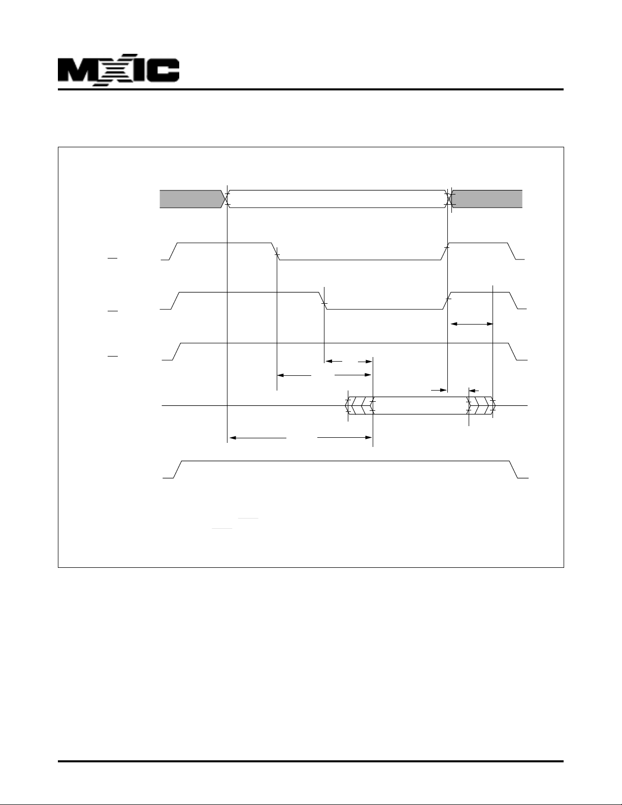
Figure 5-1. NORMAL READ TIMING WAVEFORMS
MX29L3211
ADDRESSES
CE
OE
WE
DATA OUT
VCC
Vcc
VIH
VIL
VIH
VIL
VIH
VIL
VIH
VIL
VOH
VOL
3.3V
GND
Power-up
HIGH Z
Standby
Device and
address selection
Outputs Enabled
ADDRESSES STABLE
tCE
tACC
tOE
Data valid
Data out valid
Standby
tOH
tDF
Vcc
Power-down
HIGH Z
P/N:PM0641
NOTE:
1. For real world application, BYTE pin should be either static high(word mode) or static low(byte mode);
dynamic switching of BYTE pin is not recommended.
REV. 0.3, NOV. 06, 2001
22
Page 23
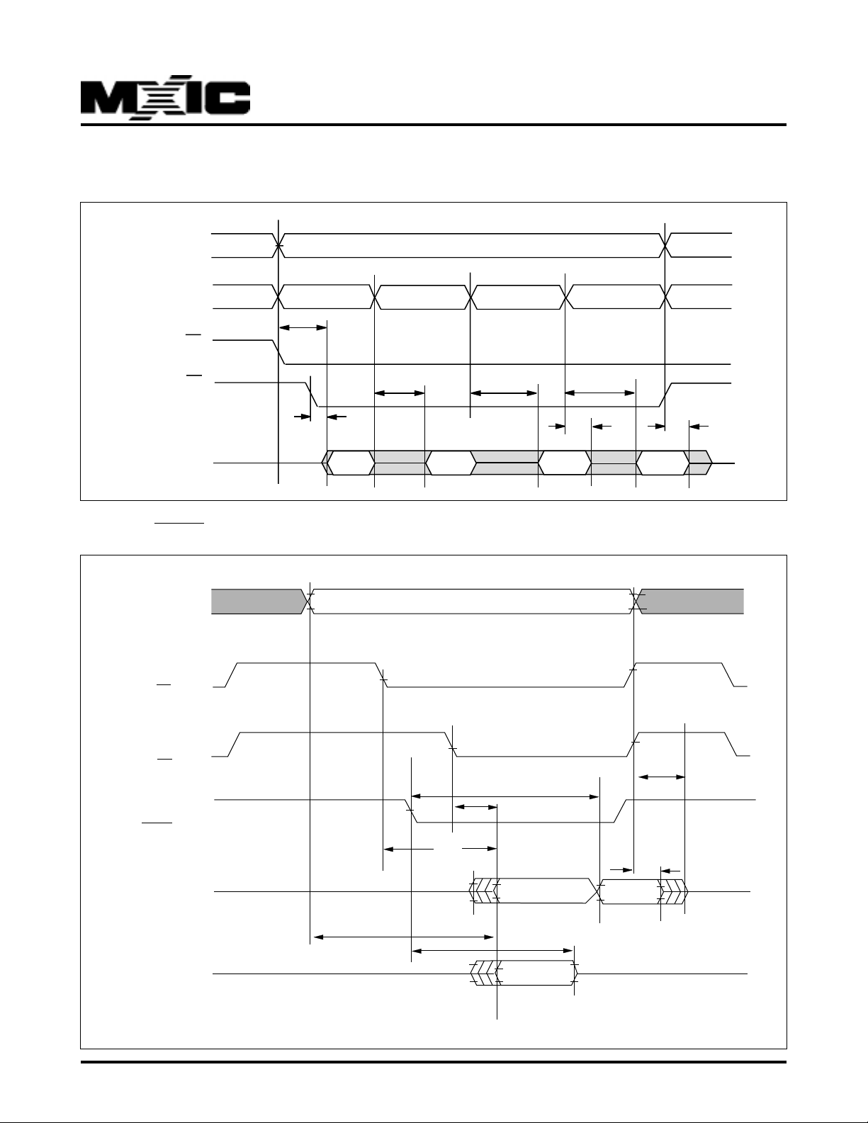
Figure 5-2. PAGE READ TIMING WAVEFORMS
MX29L3211
A3-A20
(A-1), A0~A2
tACC
CE
OE
tOE
DATA OUT
Figure 6. BYTE TIMING WAVEFORMS
VIH
ADDRESSES
VIL
VALID ADDRESS
tPA
ADDRESSES STABLE
tPA
tPA
tOH tDF
DATA(Q0-Q7)
DATA(Q8-Q15)
P/N:PM0641
CE
OE
BYTE
VIH
VIL
VIH
VIL
VIH
VIL
VOH
VOL
VOH
VOL
HIGH Z
HIGH Z
tACC
23
tCE
tOE
tBACC
tBHZ
Data Output
Data Output
tOH
Data Output
tDF
HIGH Z
HIGH Z
REV. 0.3, NOV. 06, 2001
Page 24

MX29L3211
AC CHARACTERISTICS -- WRITE/ERASE/PROGRAM OPERATIONS
29L3211-10 29L3211-12
SYMBOL DESCRIPTION MIN. MAX. MIN. MAX. UNIT
tWC Write Cycle Time 120 120 ns
tAS Address Setup Time 0 0 ns
tAH Address Hold Time 60 60 ns
tDS Data Setup Time 50 50 ns
tDH Data Hold Time 10 10 ns
tOES Output Enable Setup Time 0 0 ns
tCES CE Setup Time 0 0 ns
tGHWL Read Recover TimeBefore Write 0 0
tCS CE Setup Time 0 0 ns
tCH CE Hold Time 0 0 ns
tWP Write Pulse Width 60 60 ns
tWPH Write Pulse Width High 40 40 ns
tBALC Byte(Word) Address Load Cycle 0.3 30 0.3 30 us
tBAL Byte(Word) Address Load Time 100 100 us
tSRA Status Register Access Time 120 120 ns
tCESR CE Setup before S.R. Read 100 100 ns
tVCS VCC Setup Time 2 2 us
P/N:PM0641
REV. 0.3, NOV. 06, 2001
24
Page 25
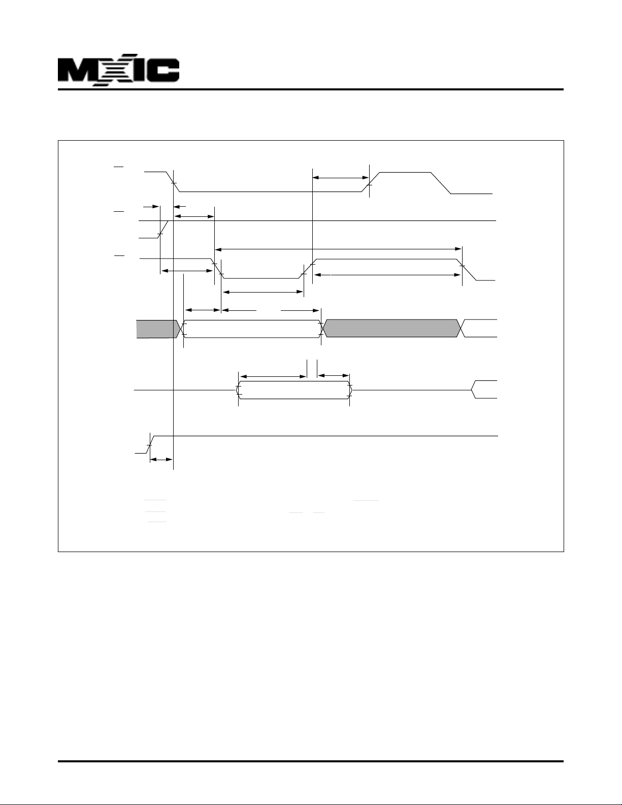
Figure 7. COMMAND WRITE TIMING WAVEFORMS
MX29L3211
CE
OE
WE
ADDRESSES
DATA
(D/Q)
VCC
tOES
tVCS
tCS
tGHWL
HIGH Z
tAS
VALID
tWP
tAH
tDS
tCH
tWC
tWPH
tDH
DIN
P/N:PM0641
NOTE:
1.BYTE pin is treated as address pin All timing specifications for BYTE pin are the same as those for address pin.
2.BYTE pin is sampled on the falling edge of WE or CE during the 3rd command write bus cycle; for real world application,
BYTE pin should be either static high(word mode) or static low(byte mode).
REV. 0.3, NOV. 06, 2001
25
Page 26
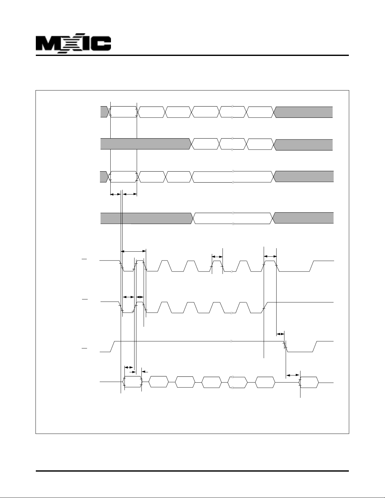
MX29L3211
Figure 8. AUTOMATIC PAGE PROGRAM TIMING WAVEFORMS
A0~A6
A-1
(Byte mode only)
A7~A14
A15~A20
CE
tAS
55H
55H
tAH
tWC
AAH
2AH
55H
55H
Word offset
Address
Low/High
Byte Select
Page Address
Page Address
tBALC
Last Word
offset Address
Last Low/High
Byte Select
tBAL
WE
OE
DATA
tWPH
tWP
tDS
tDH
AAH 55H
A0H SRD
Write
Data
NOTE:
1.Please refer to page 9 for detail page program operation.
tCES
tSRA
Last Write
Data
P/N:PM0641
REV. 0.3, NOV. 06, 2001
26
Page 27
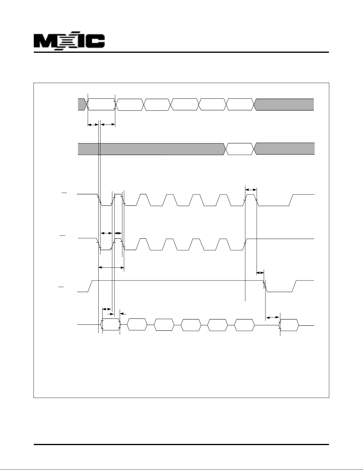
MX29L3211
Figure 9. AUTOMATIC SECTOR/CHIP ERASE TIMING WAVEFORMS
A0~A14
A16~A20
CE
WE
5555H 2AAAH 5555H
tAS
tAH
tWPH
tWP
tWC
5555H
2AAAH */5555H
SA/*
tCESR
tCES
P/N:PM0641
OE
DATA
tDS
tDH
AAH 55H
80H
NOTES:
1."*" means "don't care" in this diagram.
2."SA" means "Sector Adddress".
27
AAH
55H 30H
tSRA
SRD
REV. 0.3, NOV. 06, 2001
Page 28
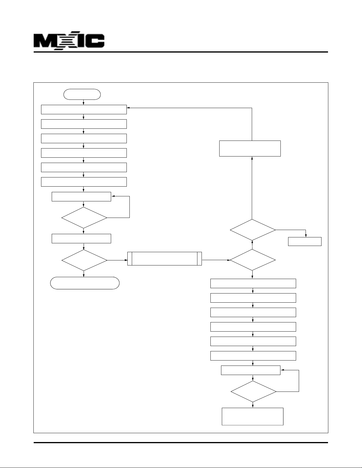
Figure 10. SECTOR PROTECTION ALGORITHM
ST ART,
PLSCNT=0
Write Data AAH Address 5555H
Write Data 55H Address 2AAAH
Write Data 60H Address 5555H
Write Data AAH Address 5555H
Write Data 55H Address 2AAAH
Write Data 20H, Sector Address*
Read Status Register
MX29L3211
Increment PLSCNT,
To Protect Sector Again
YES
NO
Verify Protect Status Flow
(Figure 12)
SR7 = 1
?
YES
Protect Sector
Operation T erminated
To
Verify Protect
Status ?
NO
Device Stays at
Read S.R. Mode
NOTE :
*Only the Top or the Bottom Sector Address is vaild in this feature.
i.e. Sector Address = (A20,A19,A18,A17,A16) = 00000B or 11111B
NO
PLSCNT
= 25 ?
NO
Data
= C2H ?
YES
Write Data AAH Address 5555H
Write Data 55H Address 2AAAH
Write Data 60H Address 5555H
Write Data AAH Address 5555H
Write Data 55H Address 2AAAH
Write Data 20H, Sector Address*
Read Status Register
YES
Device Failed
P/N:PM0641
28
SR7 = 1
?
YES
Sector Protected,Operation
Done, Device Stays at
Verify Sector Protect Mode
NO
REV. 0.3, NOV. 06, 2001
Page 29
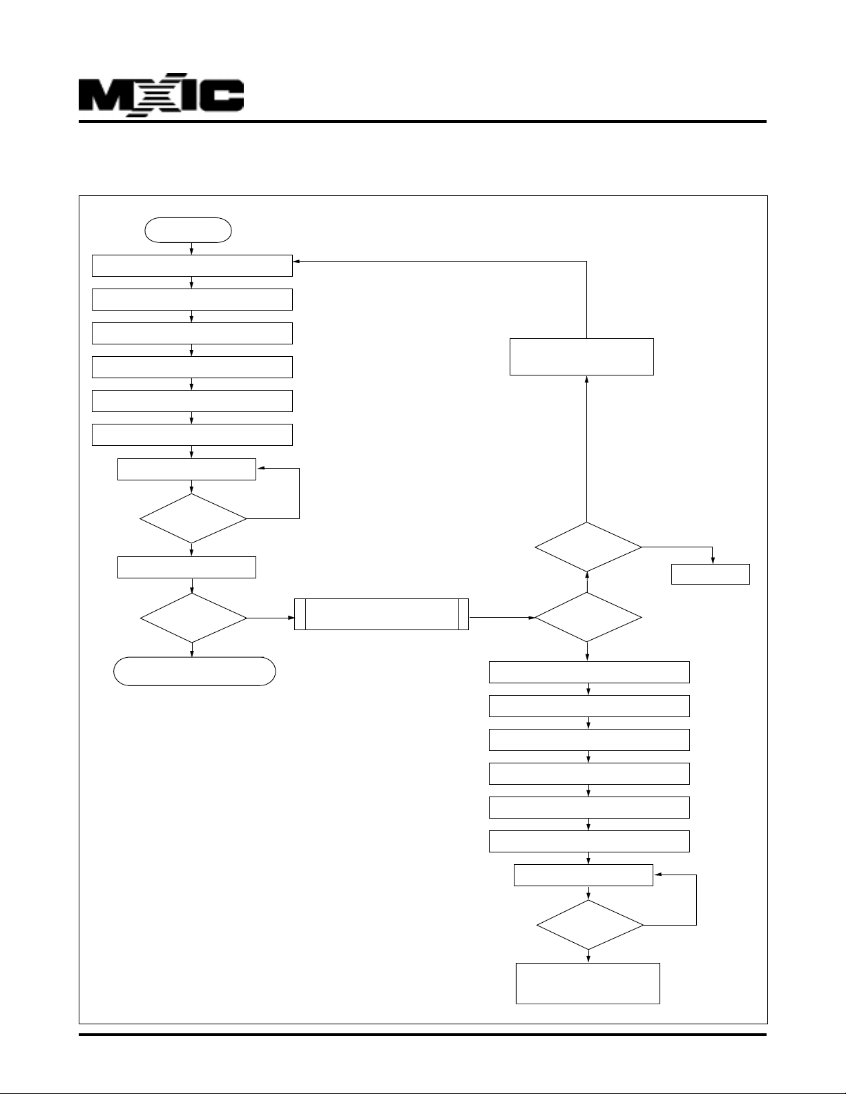
Figure 11. SECTOR UNPROTECT ALGORITHM
ST ART,
PLSCNT=0
Write Data AAH Address 5555H
Write Data 55H Address 2AAAH
Write Data 60H Address 5555H
Write Data AAH Address 5555H
Write Data 55H Address 2AAAH
Write Data 40H, Sector Address*
Read Status Register
MX29L3211
Increment PLSCNT,
To Unprotect Sector Again
YES
NO
Verify Protect Status Flow
(Figure 12)
SR7 = 1
?
YES
Protect Sector
Operation T erminated
To
Verify Protect
Status ?
NO
Device Stays at
Read S.R. Mode
NOTE :
*Only the Top or the Bottom Sector Address is vaild in this feature.
i.e. Sector Address = (A20,A19,A18,A17,A16) = 00000B or 11111B
NO
PLSCNT
= 25 ?
NO
Data
= 00H ?
YES
Write Data AAH Address 5555H
Write Data 55H Address 2AAAH
Write Data 60H Address 5555H
Write Data AAH Address 5555H
Write Data 55H Address 2AAAH
Write Data 40H, Sector Address*
Read Status Register
YES
Device Failed
P/N:PM0641
29
SR7 = 1
?
YES
Sector Unprotected,Operation
Done, Device Stays at
Verify Sector Protect Mode
NO
REV. 0.3, NOV. 06, 2001
Page 30
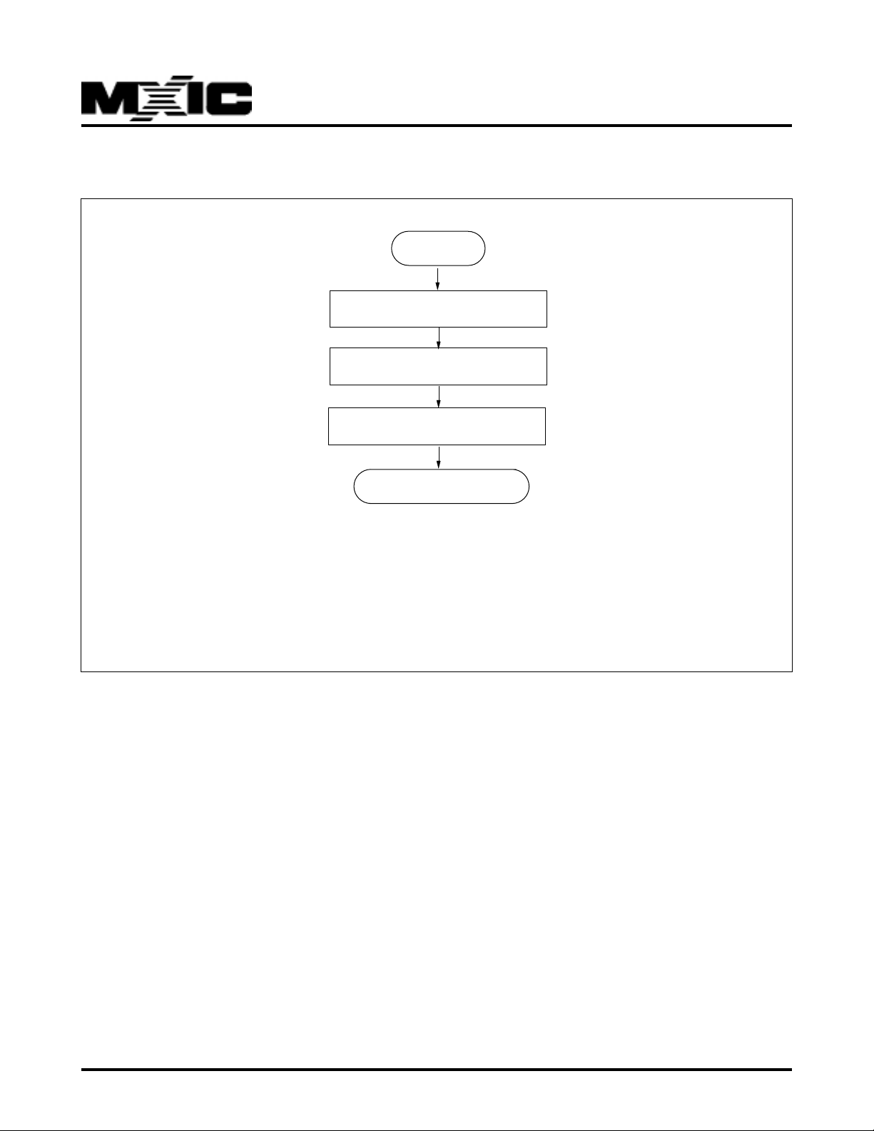
Figure 12. VERIFY SECTOR PROTECT FLOW CHART
START
Write Data AAH, Address 5555H
Write Data 55H, Address 2AAAH
Write Data 90H, Address 5555H
Ptoect Status Read*
MX29L3211
* 1. Protect Status:
Data Outputs C2H as Protected Sector Verified Code.
Data Outputs 00H as Unprotected Sector Verified Code.
2. Sepecified address will be either
(A20,A19,A18,A17,A16,A1,A0) = (0000010) or (1111110),
the rest of the address pins are don't care.
3. Silicon ID can be read via this Flow Chart.
Refer to Table 4.
P/N:PM0641
REV. 0.3, NOV. 06, 2001
30
Page 31
MX29L3211
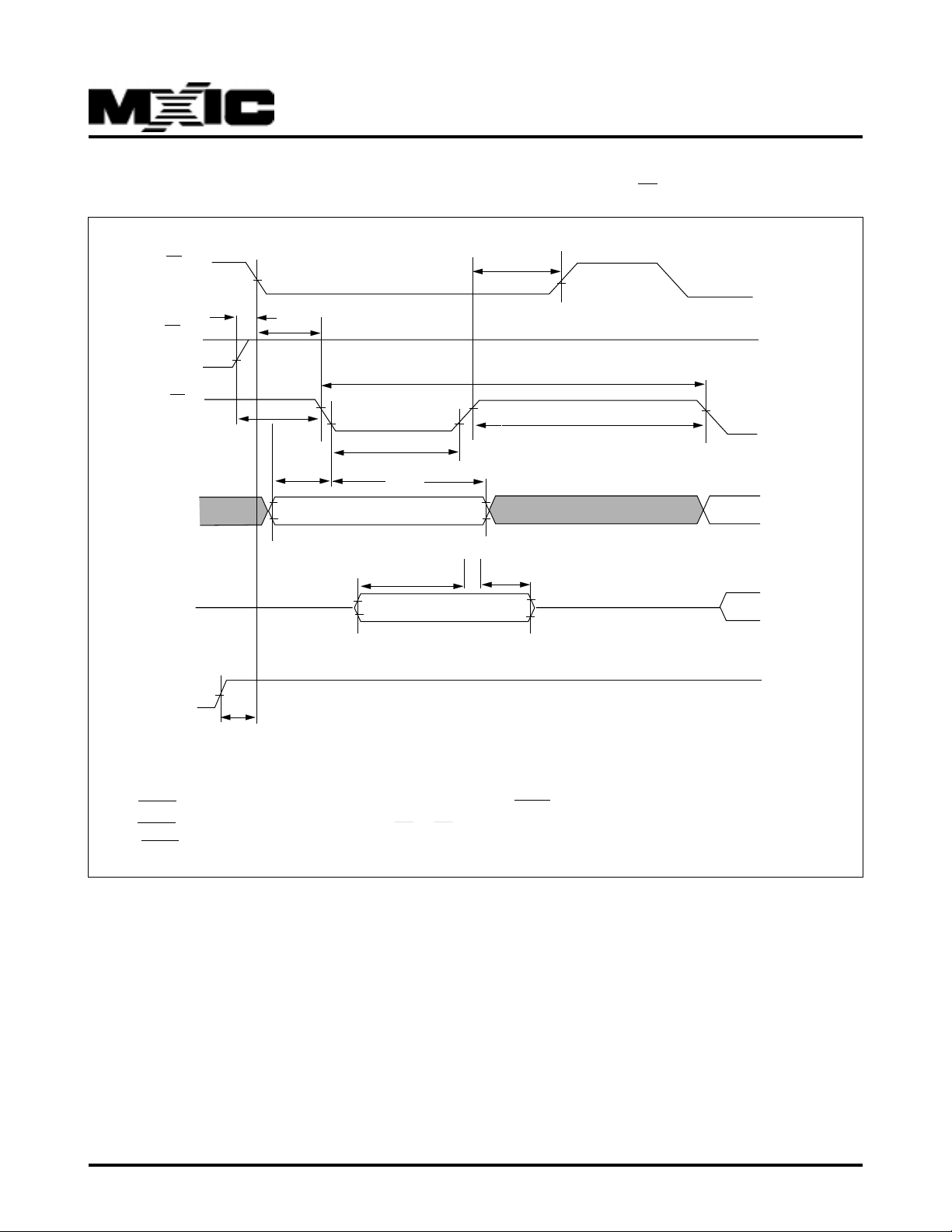
Figure 13. COMMAND WRITE TIMING WAVEFORMS(Alternate CE Controlled)
WE
OE
CE
ADDRESSES
DATA
(D/Q)
VCC
tOES
tVCS
tWS
tGHWL
HIGH Z
tAS
VALID
tCP
tAH
tDS
tWH
tWC
tCPH
tDH
DIN
NOTE:
1. BYTE pin is treated as Address pin. All timing specifications for BYTE pin are the same as those for address pin.
2. BYTE pin is sampled on the falling edge of WE or CE during the 3rd command write bus cycle; for real world applicaton,
BYTE pin should be either static high(word mode) or static low(byte mode).
P/N:PM0641
31
REV. 0.3, NOV. 06, 2001
Page 32
MX29L3211
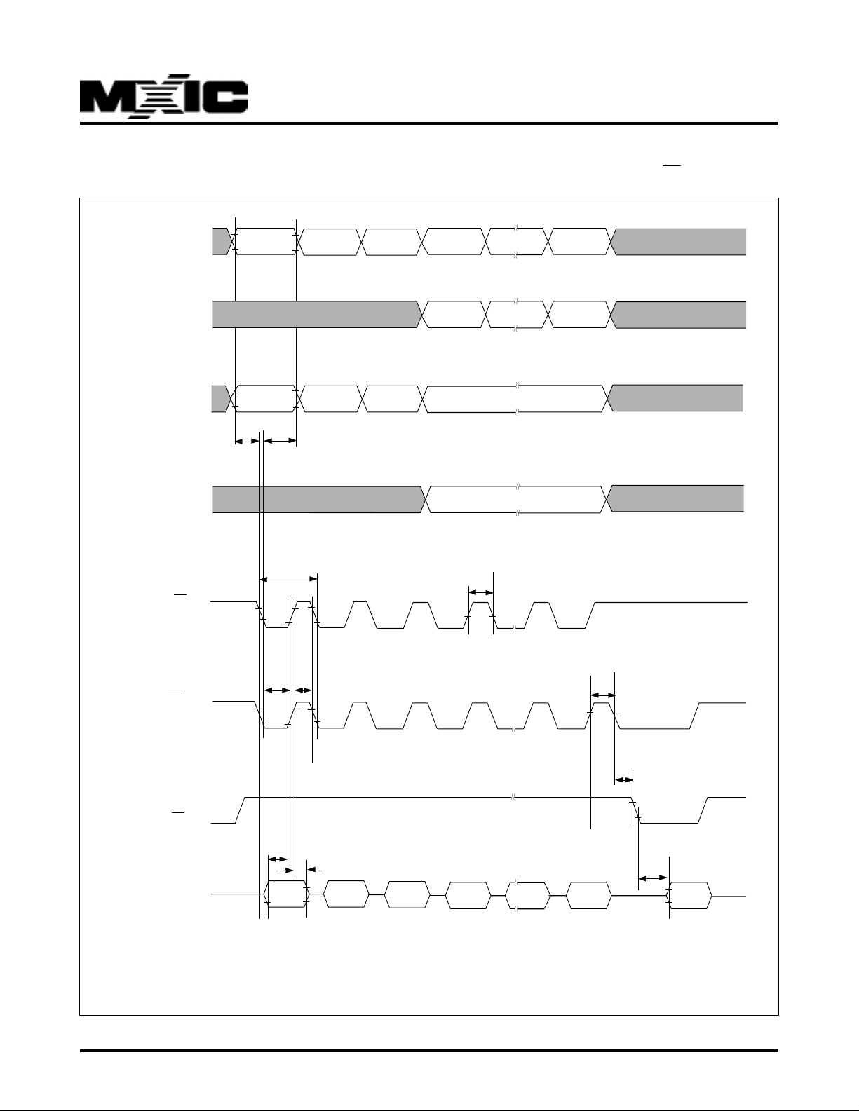
Figure 14. AUTOMATIC PAGE PROGRAM TIMING WAVEFORM(Alternate CE Controlled)
A0~A6
A-1
(Byte Mode Only)
A7~A14
A15~A20
WE
tAS
55H
55H
tAH
tWC
AAH
2AH
55H
55H
Word offset
Address
Low/High
Byte Select
Page Address
Page Address
tBALC
Last Word
Offset Address
Last Low/High
Byte Select
P/N:PM0641
CE(1)
OE
DATA
tCPH
tCP
tDS
tDH
AAH 55H
A0H SRD
Write
Data
NOTE:
1.Please refer to page 9 for detail page program operation.
32
tBAL
tCES
tSRA
Last Write
Data
REV. 0.3, NOV. 06, 2001
Page 33
MX29L3211
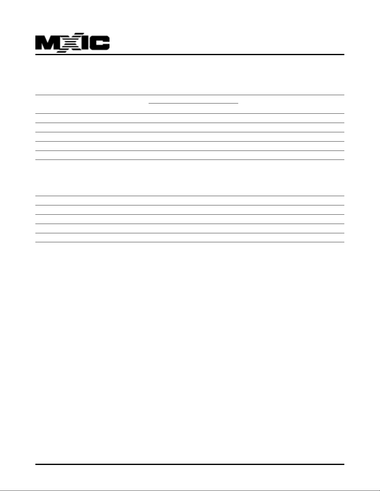
ERASE AND PROGRAMMING PERFORMANCE
LIMITS
PARAMETER MIN. TYP. MAX. UNITS
Chip/Sector Erase Time 200 2000 ms
Page Programming Time 5 50 0 ms
Chip Programming Time 80 800 sec
Byte Program Time 20 2000 us
Erase/Program Cycles 10,000 Cycles
LATCHUP CHARACTERISTICS
MIN. MAX.
Input Voltage with respect to GND on all pins except I/O pins -1.0V 6.6V
Input Voltage with respect to GND on all I/O pins -1.0V Vcc + 1.0V
Current -100mA +100mA
Includes all pins except Vcc. Test conditions: Vcc = 3.3V, one pin at a time.
P/N:PM0641
REV. 0.3, NOV. 06, 2001
33
Page 34

MX29L3211
ORDERING INFORMATION
PLASTIC PACKAGE
PART NO. ACCESS TIME OPERATING CURRENT STANDBY CURRENT PACKAGE
(ns) MAX.(mA) MAX.(uA)
MX29L3211MC-10 10 0 50 20 44 Pin SOP
MX29L3211TC-10 100 50 20 48 Pin TSOP
P/N:PM0641
REV. 0.3, NOV. 06, 2001
34
Page 35
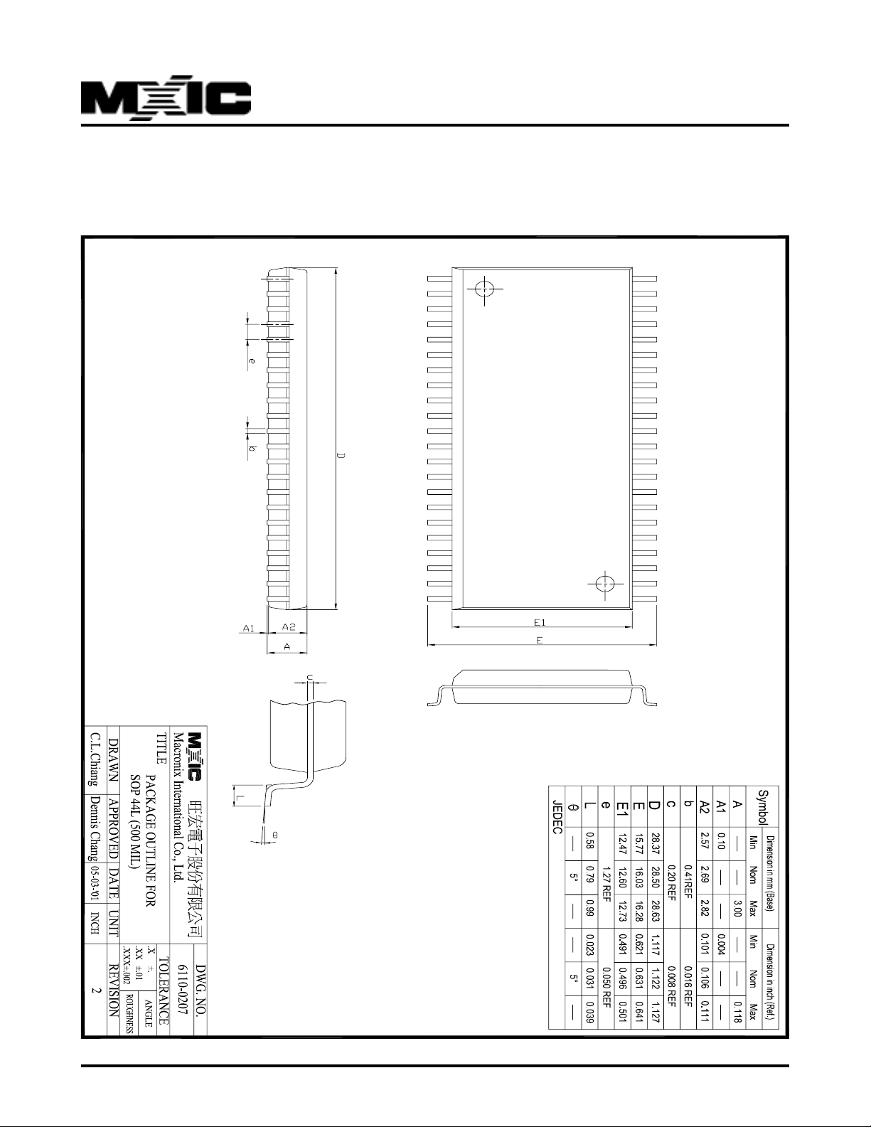
PACKAGE INFORMATION
44-PIN PLASTIC SOP
MX29L3211
P/N:PM0641
REV. 0.3, NOV. 06, 2001
35
Page 36
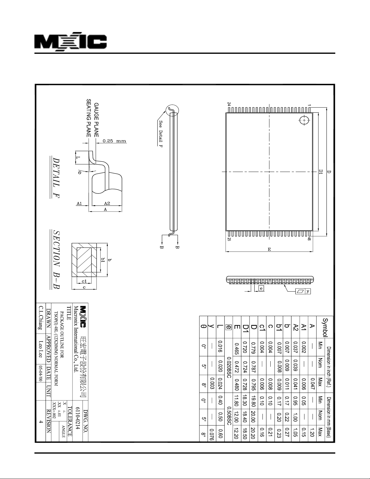
48-PIN PLASTIC TSOP(NORMAL TYPE)
MX29L3211
P/N:PM0641
REV. 0.3, NOV. 06, 2001
36
Page 37

MX29L3211
HISTORY STORY
Revision Description Page Date
0.1 Add 48TSOP P1,2 JAN/19/2000
Add order information P34
Add package information P35
0.2 Del Fast pagemode access time:30ns P1 MAY/15/2000
Modify 29L3211-10 tPA:30-->50 ; 29L3211-12 tPA:40-->50 P 21
Add tPA=50ns 1 TTL gate + 100pF ; tPA=40ns 1 TTL gate + 30pF P21
0.3 To modify Package Information P35~36 NOV/06/2001
P/N:PM0641
REV. 0.3, NOV. 06, 2001
37
Page 38

MX29L3211
MACRONIX INTERNATIONAL CO., LTD.
HEADQUARTERS:
TEL:+886-3-578-6688
FAX:+886-3-563-2888
EUROPE OFFICE:
TEL:+32-2-456-8020
FAX:+32-2-456-8021
JAPAN OFFICE:
TEL:+81-44-246-9100
FAX:+81-44-246-9105
SINGAPORE OFFICE:
TEL:+65-348-8385
FAX:+65-348-8096
TAIPEI OFFICE:
TEL:+886-2-2509-3300
FAX:+886-2-2509-2200
MACRONIX AMERICA, INC.
TEL:+1-408-453-8088
FAX:+1-408-453-8488
CHICAGO OFFICE:
TEL:+1-847-963-1900
FAX:+1-847-963-1909
http : //www.macronix.com
MACRONIX INTERNATIONAL CO., LTD. reserves the right to change product and specifications without notice.
38
 Loading...