

Page 1
FEATURES
PRELIMINARY
MX27C1610
16M-BIT [2M x 8/1M x 16] CMOS OTP ROM
• 2M x 8 or 1M x 16 organization
• 5V Vcc for Read operation
• 10V Vpp Programming operation
• Fast access time: 100/120 ns
• Totally static operation
GENERAL DESCRIPTION
The MX27C1610 is a 16M-bit, One Time Progr ammable
Read Only Memory. It is organized as 2M x 8 or 1M x
16 and has a static standby mode, and features fast
programming. F or programming outside from the system, existing EPROM progr ammers may be used. The
MX27C1610 supports a intelligent fast programming al-
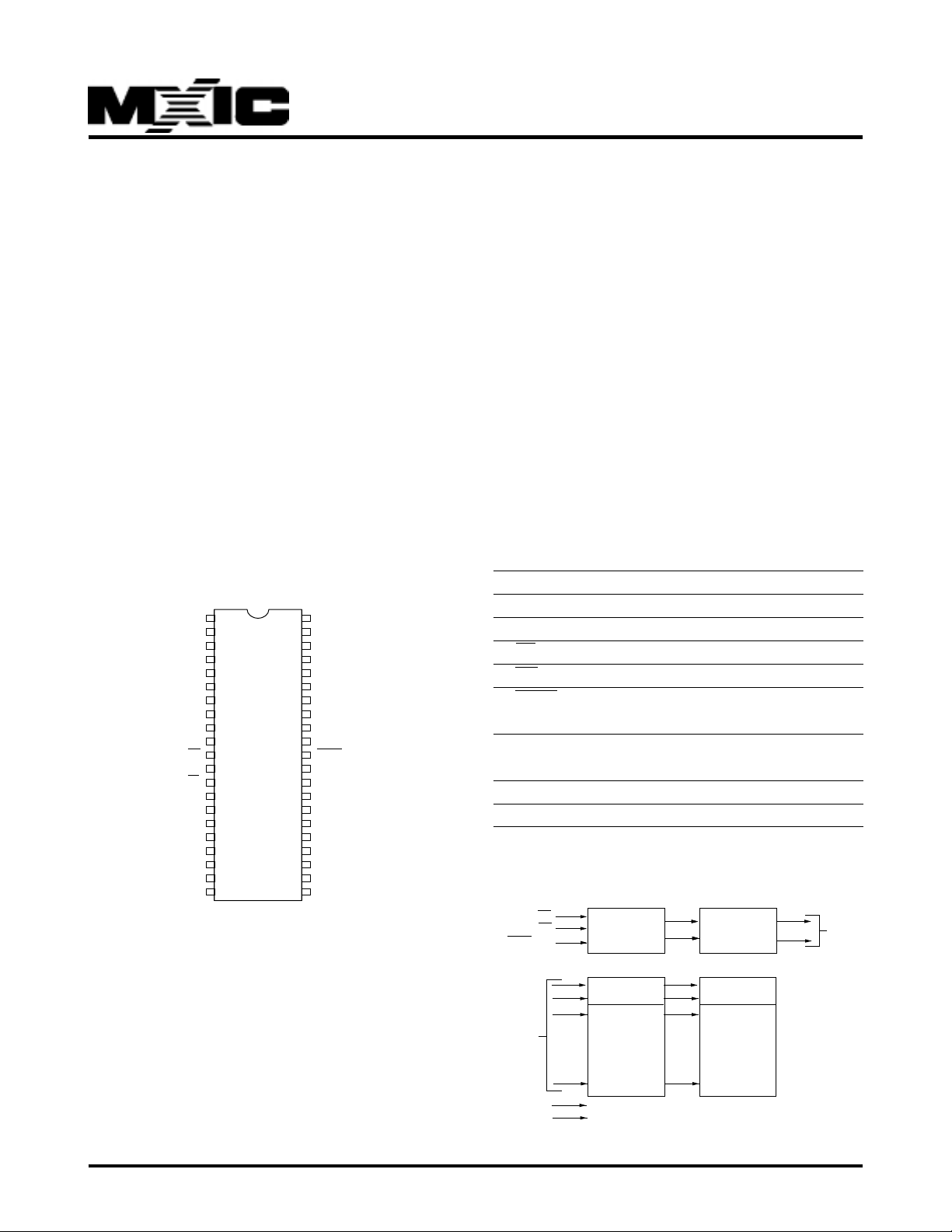
PIN CONFIGURATIONS
PDIP
A18
A17
CE
GND
OE
Q0
Q8
Q1
Q9
Q2
Q10
Q3
Q11
1
2
A7
3
A6
4
A5
5
A4
6
A3
7
A2
8
A1
9
A0
10
11
12
MX27C1610
13
14
15
16
17
18
19
20
21
42
41
40
39
38
37
36
35
34
33
32
31
30
29
28
27
26
25
24
23
22
A19
A8
A9
A10
A11
A12
A13
A14
A15
A16
BYTE/VPP
GND
Q15/A-1
Q7
Q14
Q6
Q13
Q5
Q12
Q4
VCC
• Completely TTL compatible
• Operating current: 60mA
• Standby current: 100uA
• Package type:
- 42 pin plastic DIP
gorithm which can result in programming time of less
than two minutes.
This One Time Programmable Read Only Memory is
packaged in industry standard 42 pin dual-in-line plastic package.
PIN DESCRIPTION
SYMBOL PIN NAME
A0~A19 Address Input
Q0~Q14 Data Input/Output
CE Chip Enable Input
OE Output Enab le Input
BYTE/VPP Word/Byte Selection
/Program Supply Voltage
Q15/A-1 Q15(Word mode)/LSB addr. (Byte
mode)
VCC Po wer Supply Pin (+5V)
GND Ground Pin
BLOCK DIAGRAM
BYTE/VPP
CE
OE
CONTROL
LOGIC
OUTPUT
BUFFERS
Q0~Q14
Q15/A-1
.
Y -DECODER
.
VCC
VSS
.
.
.
.
.
.
X-DECODER
A0~A19
ADDRESS
INPUTS
P/N:PM0593 REV. 1.3, APR. 26, 2000
.
.
.
.
.
.
.
.
Y -DECODER
16M BIT
CELL
MAXTRIX
1
Page 2
MX27C1610
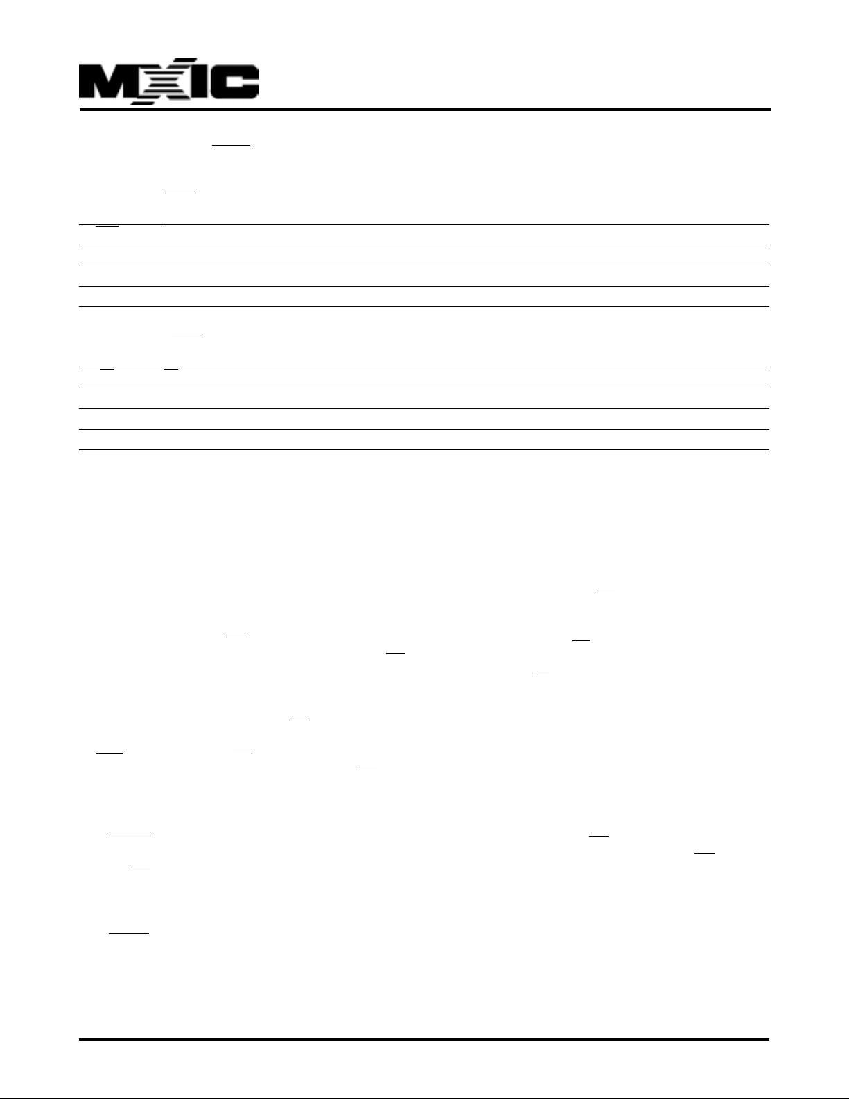
TRUTH TABLE OF BYTE FUNCTION
BYTE MODE(BYTE = GND)
CE OE Q15/A-1 MODE Q0-Q7 SUPPLY CURRENT
H X X Non selected High Z Standby(ICC2)
L H X Non selected High Z Operating(ICC1)
L L A-1 input Selected DOUT Operating(ICC1)
WORD MODE(BYTE = VCC)
CE OE Q15/A-1 MODE Q0-Q7 SUPPLY CURRENT
H X High Z Non selected High Z Standby(ICC2)
L H High Z Non selected High Z Operating(ICC1)
L L DOUT Selected DOUT Oper ating(ICC1)
NOTE : X = H or L
FUNCTIONAL DESCRIPTION
READ MODE
The MX27C1610 has two control functions, both of which
must be logically satisfied in order to obtain data at the
outputs. Chip Enable (CE) is the power control and
should be used for device selection. Output Enable (OE)
is the output control and should be used to gate data to
the output pins, independent of device selection. Assuming that addresses are stable, address access time
(tACC) is equal to the delay from CE to output (tCE).
Data is availab le at the outputs tOE after the falling edge
of OE's, assuming that CE has been LOW and addresses have been stable for at least tACC - t OE.
WORD-WIDE MODE
With BYTE/VPP at VCC ± 0.2V outputs Q0-7 present
data Q0-7 and outputs Q8-15 present data Q8-15, after
CE and OE are appropriately enabled.
BYTE-WIDE MODE
With BYTE/VPP at GND ± 0.2V, outputs Q8-15 are tristated. If Q15/A-1 = VIH, outputs Q0-7 present data
bits Q8-15. If Q15/A-1 = VIL, outputs Q0-7 present data
bits Q0-7.
STANDBY MODE
The MX27C1610 has a CMOS standby mode which reduces the maximum VCC current to 100 uA. It is placed
in CMOS standby when CE is at VCC ± 0.2V. The
MX27C1610 also has a TTL-standby mode which reduces the maximum VCC current to 4 mA. It is placed
in TTL-standby when CE is at VIH. When in standby
mode, the outputs are in a high-impedance state, independent of the OE input.
TWO-LINE OUTPUT CONTROL FUNCTION
To accommodate multiple memory connections, a twoline control function is provided to allow f or:
1. Lo w memory power dissipation,
2. Assur ance that output b us contention will not occur.
It is recommended that CE be decoded and used as
the primary device-selecting function, while OE be made
a common connection to all devices in the array and
connected to the READ line from the system control
bus. This assures that all deselected memory devices
are in their low-power standby mode and that the output pins are only active when data is desired from a
particular memory device.
P/N:PM0593
REV. 1.3, APR. 26, 2000
2
Page 3
MX27C1610
SYSTEM CONSIDERA TIONS
During the switch between active and standby conditions, transient current peaks are produced on the rising and falling edges of Chip Enable . The magnitude of
these transient current peaks is dependent on the output capacitance loading of the device. At a minimum, a
0.1 uF ceramic capacitor (high frequency, low inherent
inductance) should be used on each device between
Vcc and GND to minimize transient effects. In addition,
to overcome the voltage drop caused by the inductive
effects of the printed circuit board traces on One Time
Programmable Read Only Memory arrays, a 4.7 uF
bulk electrolytic capacitor should be used between VCC
and GND for each eight devices. The location of the
capacitor should be close to where the power supply is
connected to the array.
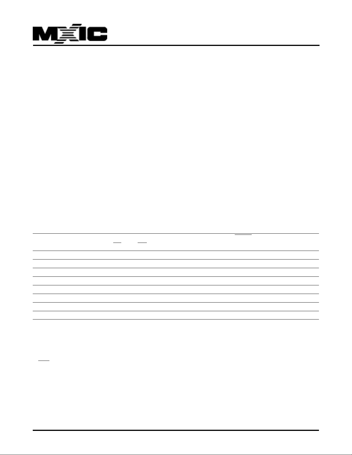
MODE SELECT T ABLE
WRITE OPERA TIONS
Commands are written to the COMMAND INTERF ACE
REGISTER (CIR) using standard microprocessor write
timings. The CIR serves as the interface between the
microprocessor and the internal chip operation. The
CIR can decipher Read Array, Read Silicon ID and Program command. In the event of a read command, the
CIR simply points the read path at either the array or
the silicon ID , depending on the specific read command
given. For a program cycle, the CIR informs the write
state machine, and the write state machine and the write
state machine will control the program sequences and
the CIR will only respond to status reads. After the
write state machine has completed its task, it will allow
the CIR to respond to its full command set. The CIR
stays at read status register mode until the microprocessor issues another valid command sequence.
Device operations are selected by writing commands
into the CIR. See command definition table belo w.
BYTE/
MODE CE OE A9 A0 Q15/A-1 VPP(5) Q8-14 Q0-7
Read (Word) (2) VIL VIL X X Q15 Out VIH Q8-14 Out Q0-7 Out
Read (Upper Byte) (2) VIL VIL X X VIH VIL High Z Q8-15 Out
Read (Lower Byte) (2) VIL VIL X X VIL VIL High Z Q0-7 Out
Output Disable (2) VIL VIH X X High Z X High Z High Z
Standby (2) VIH X X X High Z X High Z High Z
Write Operation (2) VIL VIH X X Q15 In VPP Q8-14 In Q0-7 In
ManufacturerID(3)(1) VIL VIL VH VIL 0B VIH 00H C2H
Device ID(3)(1) VIL VIL VH VIH 0B VIH 00H 6AH
NOTES:
1. VH = 10V ± 0.5V
2. X Either VIL or VIH.
3. A1= VIL, other address lines not specified are at "X" states
4. See DC Programming Characteristics for VPP voltages.
5. BYTE/VPP is intended for operation under DC Voltage conditions only. VPP=10V± 0.5V for write operation
P/N:PM0593
REV. 1.3, APR. 26, 2000
3
Page 4
MX27C1610
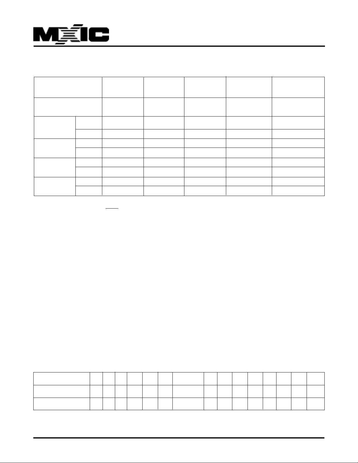
COMMAND DEFINITIONS OF WRITE OPERATION TABLE
Command Read/ Silicon Page/Byte Read Clear
Sequence Reset ID Read Program Status Reg. Status Reg.
Bus Write 4 4 4 4 3
Cycles Req'd
First Bus Addr 5555H 5555H 5555H 5555H 5555H
Write Cycle Data AAH AAH AAH AAH AAH
Second Bus Addr 2AAAH 2AAAH 2AAAH 2AAAH 2AAAH
Write Cycle Data 55H 55H 55H 55H 55H
Third Bus Addr 5555H 5555H 5555H 5555H 5555H
Write Cycle Data F0H 90H A0H 70H 50H
Fourth Bus Addr RA 00H/01H PA X
Read/Write Cycle Data RD C2H/6AH PD SRD
NOTES:
1. In the write operation mode, BYTE/VPP should be set to 10V±0.5V.
2. 5555H and 2AAAH address command codes stand for Hex number starting from A0 to A14.
3. RA=Address of the memory location to be read.
RD=Data read from location RA during read operation.
PA=Address of the memory location to be programmed.
PO=Data to be programmed at location PA.
DEVICE OPERATION
SILICON ID READ
The Silicon ID Read mode allows the reading out of a
binary code from the device and will identify its manufacturer and type. This mode is intended for use by
programming equipment for the purpose of automatically matching the device to be programmed with its
T o activ ate this mode, the programming equipment must
force VID (10V±o .5V) on address pin A9. Two identifier
bytes may then be sequenced from the de vice outputs
by toggling address A0 from VIL to VIH. All addresses
are don't cares except A0 and A1.
corresponding programming algorithm. This mode is
functional over the entire temperature r ange of the device.
The manufacturer and device codes may also be read
via the command register, for instances when the
MX27C1610 is programmed in a system without access
to high voltage on the A9 pin.
MX27C1610 Silion ID Codes
Type A19 A18A17A
Manufacturer Code** X X X X VIL VIL C2H* 1 1 0 0 0 0 1 0
Device Code** X X X X VIL VIH 6AH* 0 1 1 0 1 0 1 0
* The high byte of the code will be 00H and low byte of the code will be C2H for Manufacturer code and 6AH of Device code.
** All other address lines not specified are also at "X" state. X=VIH or VIL.
A1A0Code(HEX) DQ7DQ6DQ5DQ4DQ3DQ2DQ1DQ
16
0
P/N:PM0593
REV. 1.3, APR. 26, 2000
4
Page 5

MX27C1610
READ/RESET COMMAND
The read or reset operation is initiated by writing the
read/reset command sequence into the command register. Microprocessor read cycles retrieve array data
from the memory . The device remains enab led for reads
until the CIR contents are altered by a valid command
sequence.
The device will automatically power-up in the read/reset state. In this case, a command sequence is not
required to read data. Standard microprocessor read
cycles will retrieve array data. This default value ensures that no spurious alteration of the memory content
occurs during the power transition. Refer to the AC Read
Characteristics and Waveforms for the specific timing
parameters.
The MX27C1610 is accessed when CE and OE are low
the data stored at the memory location determined by
the address pins is asserted on the outputs. The outputs are put in the high impedance state whenever CE
or OE is high. This dual line control gives designers
flexibility in pre venting b us contention.
Note that the read/reset command is not valid when program is in progress.
PAGE PROGRAM
The device is set up in the programming mode when
the programming Voltage Vpp=10V is applied with
Vcc=5V, and OE=VIH.
WORD-WIDE LOAD
Word loads are used to enter the 128 bytes(64 w ords)
of a page to be programmed or the software codes for
data protection. A word load is perf ormed by applying a
low pulse on the CE input with CE and OE high. The
address is latched on the falling edge of CE. The data is
latched by the rising edge of CE.
PROGRAM
The device is programmed on a page basis . Once the
bytes of a page are loaded into the device, they are
simultaneously programmed during the internal pro-
gramming period. After the first data word has been
loaded into the device, successive w ords are entered in
the same manner. The time between word loads must
be less than 30us otherwise the load period could be
teminated. A6 to A19 specify the page address, i.e.,
the device is page-aligned on 128 bytes(64
words)boundary . The page address must be valid dur-
ing each high to low transition of CE. A0 to A5 specify
the word address withih the page. The word may be
loaded in any order; sequential loading is not required.
If a high to low transition of CE is not detected whithin
100us of the last low to high transition, the load period
will end and the internal programming period will start.
The Auto page program terminates when status on Q7
is "1" at which time the device sta ys at read status reg-
ister mode until the CIR contents are altered by a valid
command sequence.
Any attempt to write to the device without the threecycle command sequence will not start the internal Write
State Machine(WSM), no data will be written to the device.
After three-cycle command (see command table) sequence is given, a word load is performed by applying a
low pulse on the CE input with CE low and OE high.
The address is latched on the falling edge of CE The
data is latched by the rising edge of CE . Maximum of
128 bytes of data may be loaded into each page b y the
same procedure as outlined in the page program section below .
P/N:PM0593
REV. 1.3, APR. 26, 2000
5
Page 6

MX27C1610
READ STATUS REGISTER
The MXIC's16 Mbit OTP ROM contains a status register which may be read to determine when a program
operation is complete, and whether that operation completed successfully . The status register may be read at
any time by writing the Read Status command to the
CIR. After writing this command, all subsequent read
operations output data from the status register until another valid command sequence is written to the CIR. A
Read Array command must be written to the CIR to return to the Read Array mode.
It should be noted that the contents of the status register are latched on the falling edge of OE or CE whichever occurs last in the read cycle. This prevents possible bus errors which might occur if the contents of the
status register change while reading the status register.
CE or OE must be toggled with each subsequent status
read, or the completion of a program operation will not
be evident.
The Status Register is the interface between the microprocessor and the Write State Machine (WSM). When
the WSM is active, this register will indicate the status
of the WSM, and will also hold the bits indicating whether
or not the WSM was successful in performing the desired operation. The WSM can set status bit4 and bit7.
Howev er , the WSM can only clear bit 7 but can not clear
bit 4. If Program fail status bit is detected, the Status
Register is not cleared until the "Clear Status Register
command" is issued. The MX27C1610 automatically outputs Status Register data when read after Page Program or Read Status Command write cycle. The internal state machine is set for reading array data upon
device pow er-up.
CLEAR STATUS REGISTER
The Program fail status bit (Q4) are set by the write
state machine, and can only be reset by the system
software. These bits can indicate various failure
conditions(see Table below). By allowing the system
software to control the resetting of these bits, several
operations may be performed (such as cumulatively
programming several pages . The status register may
then be read to determine if an error occurred during
that programming series. This adds flexibility to the
way the de vice may be programmed. Additionally, once
the program fail bit happens, the prog ram operation can
not be performed further. The program fail bit must be
reset by system software before further page program
are attempted. To clear the status register, the Clear
Status Register command is written to the CIR. Then,
any other command may be issued to the CIR. Note
again that before a read cycle can be initiated, a Read
command must be written to the CIR to specify whether
the read data is to come from the Array , Status Register
or Silicon ID .
P/N:PM0593
REV. 1.3, APR. 26, 2000
6
Page 7
MX27C1610
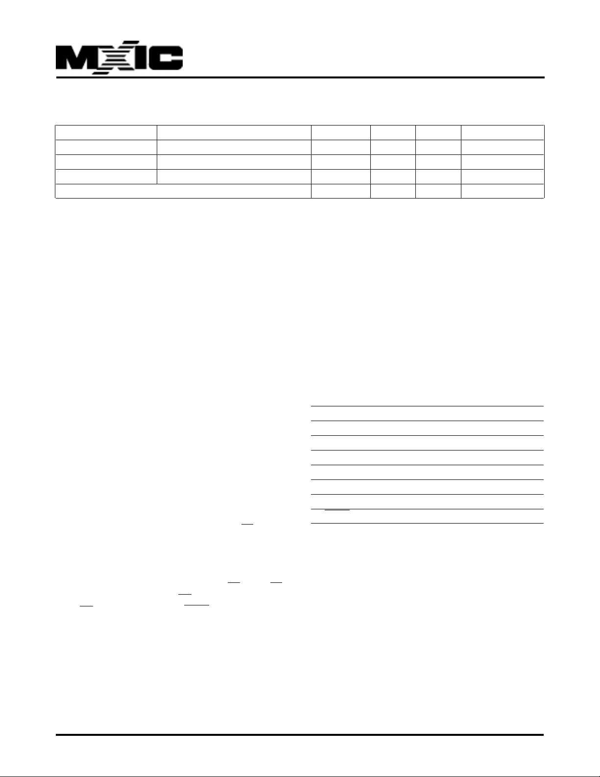
STATUS REGISTER TABLE
ST ATUS NOTES Q7 Q4 Q3
IN PROGRESS PROGRAM 1,2 0 0 0
COMPLETE PROGRAM 1,2 1 0 0
FAIL PROGRAM 1,3 1 1 0
AFTER CLEARING ST ATUS REGISTER 10 0
NOTES:
1. Q7 : WRITE STATE MACHINE STATUS
1 = READY, 0 = BUSY
Q4 : PROGRAM FAIL STATUS
1 = FAIL IN PROGRAM, 0 = SUCCESSFUL PROGRAM
Q3=0 = RESERVED FOR FUTURE ENHANCEMENTS.
These bits are reserved for future use ; mask them out when polling the Status Register.
2. PROGRAM STATUS is for the status during Page Programming.
3. FAIL STATUS bit(Q4) is provied during Page Program mode.
LOW VCC WRITE INHIBIT
To avoid initiation of a write cycle during VCC power-up
and power-down, a write cycle is locked out for VCC
less than VLK O(= 3.2V , typically 3.5V). If VCC < VLK O,
the command register is disabled and all internal program circuits are disabled. Under this condition the
device will reset to the read mode. Subsequent writes
will be ignored until the VCC le vel is greater than VLK O.
It is the user's responsibility to ensure that the control
pins are logically correct to prevent unintentional write
when VCC is abo v e VLKO.
WRITE PULSE "GLITCH" PROTECTION
Noise pulses of less than 10ns (typical) on CE will not
initiate a write cycle.
LOGICAL INHIBIT
Writing is inhibited by holding any one of OE = VIL,CE =
VIH. To initiate a write cycle CE must be a logical zero
while OE is a logical one, and BYTE/VPP=10V.
ELECTRICAL SPECIFICATIONS
ABSOLUTE MAXIMUM RATINGS
RATING V ALUE
Ambient Operating Temperature 0°C to 70°C
Storage T emperature -65°C to 125°C
Applied Input Voltage -0.5V to 7.0V
Applied Output Voltage -0.5V to 7.0V
VCC to Ground Potential -0.5V to 7.0V
A9 -0.5V to 13.5V
BYTE/VPP -0.5V to 12.0V
NOTICE:
Stresses greater than those listed under ABSOLUTE MAXI-
MUM RATINGS may cause permanent damage to the de-
vice. This is stress rating only and functional operational
sections of this specification is not implied. Exposure to ab-
solute maximum rating conditions for extended period may
affect reliability.
NOTICE:
Specifications contained within the following tables are sub-
ject to change.
P/N:PM0593
REV. 1.3, APR. 26, 2000
7
Page 8
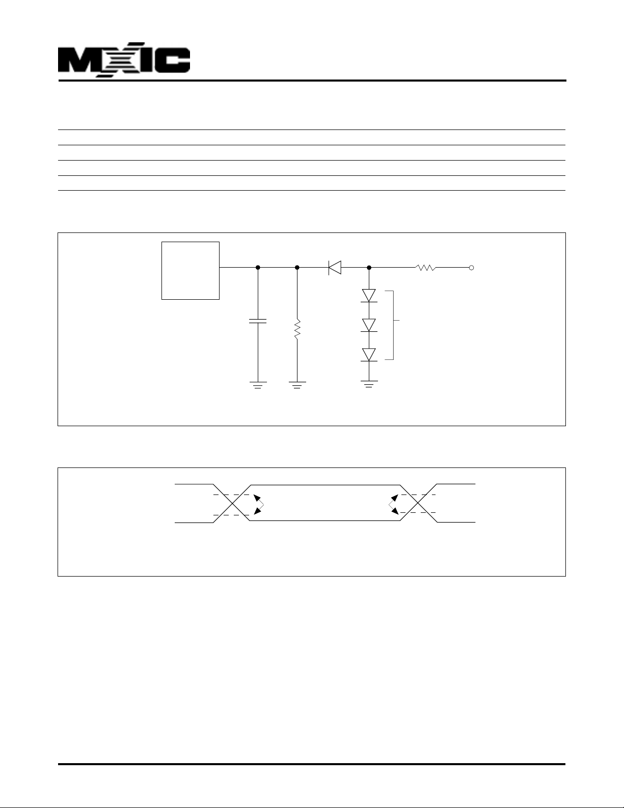
MX27C1610
CAPACITANCE TA = 25
°°
°C, f = 1.0 MHz
°°
SYMBOL PARAMETER MIN. TYP. MAX. UNIT CONDITIONS
CIN Input Capacitance 14 pF VIN = 0V
CVPP VPP Capacitance 20 pF VPP=0V
COUT Output Capacitance 16 pF VOUT = 0V
SWITCHING TEST CIRCUITS
DEVICE
UNDER
TEST
CL
1.2K ohm
1.6K ohm
DIODES = IN3064
OR EQUIVALENT
+5V
CL = 100 pF Including jig capacitance
SWITCHING TEST WA VEFORMS
2.4V
0.45V
AC TESTING: Inputs are driven at 2.4V for a logic "1" and 0.45V for a logic "0".
Input pulse rise and fall times are < 10ns.
INPUT
2.0V
0.8V
TEST POINTS
2.0V
0.8V
OUTPUT
P/N:PM0593
REV. 1.3, APR. 26, 2000
8
Page 9
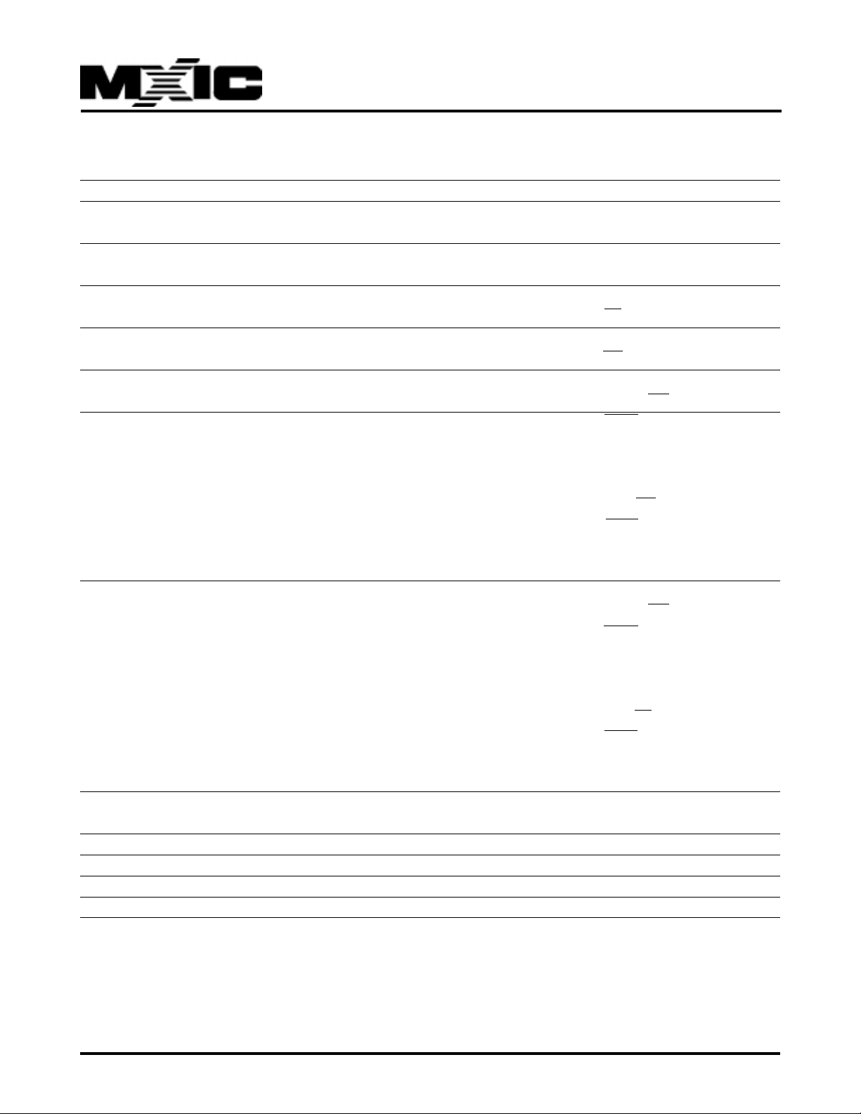
MX27C1610
DC CHARACTERISTICS TA = 0
SYMBOL PARAMETER NOTES MIN. TYP. MAX. UNITS TEST CONDITIONS
ILI Input Leakage 1 ±10 uA VCC = VCC Max
Current VIN = VCC or GND
ILO Output Leakage 1 ±10 uA VCC = VCC Max
Current VIN = VCC or GND
ISB1 VCC Standby 1 1 100 uA VCC = VCC Max
Current(CMOS) CE = VCC±0.2V
ISB2 VCC Standby 2 4 mA VCC = VCC Max
Current(TTL) CE = VIH
ICC1 VCC Read 1 50 60 mA VCC = VCC Max
Current CMOS: CE = GND± 0.2V
ICC2 VCC Read 1 30 35 mA VCC = VCC Max,
Current CMOS: CE = GND± 0.2V
ICC4 VCC Program 1 30 50 mA Program in Progress
Current
VIL Input Low Voltage 2 -0.3 0.8 V
VIH Input High Voltage 3 2.4 VCC+0.3 V
VOL Output Low Voltage 0.45 V IOL = 2.1mA
VOH Output High Voltage 2.4 V IOH = -2mA
°°
°C to 70
°°
°°
°C, VCC = 5V
°°
±±
±10%
±±
BYTE/VPP = GND±0.2V or
VCC± 0.2V
Inputs = GND±0.2V or
VCC± 0.2V
TTL : CE = VIL,
BYTE/VPP = VIL or VIH
Inputs = VIL or VIH,
f = 10MHz, IOUT = 0 mA
BYTE/VPP = VCC±0.2V or
GND± 0.2V
Inputs = GND±0.2V or
VCC±0.2V
TTL: CE= VIL,
BYTE/VPP = VIH or VIL
Inputs = VIL or VIH,
f = 5MHz, IOUT = 0mA
NOTES:
1. All currents are in RMS unless otherwise noted. Typical values at VCC = 5.0V, T = 25°C. These currents are valid for all
product versions (package and speeds).
2. VIL min. = -1.0V for pulse width £ 50ns.
VIL min. = -2.0V for pulse width £ 20ns.
3. VIH max. = VCC + 1.5V for pulse width £ 20ns. If VIH is over the specified maximum value, read operation cannot be
guaranteed.
P/N:PM0593
9
REV. 1.3, APR. 26, 2000
Page 10
MX27C1610
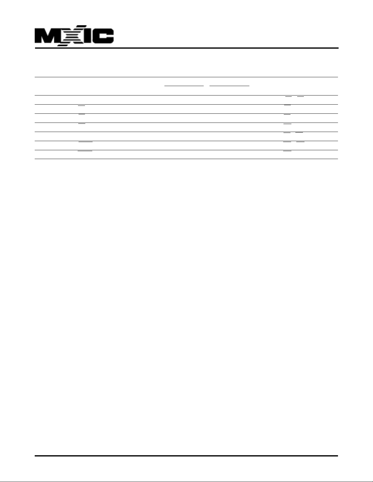
AC CHARACTERISTICS --- READ OPERATIONS
27C1610-10 27C1610-12
SYMBOL DESCRIPTIONS MIN. MAX. MIN. MAX. UNIT CONDITIONS
tACC Address to Output Delay 100 120 ns CE=OE=VIL
tCE CE to Output Delay 100 120 ns OE=VIL
tOE OE to Output Delay 50 50 ns CE=VIL
tDF OE High to Output in High Z 0 35 0 35 ns CE=VIL
tOH Address to Output hold 0 0 ns CE=OE=VIL
tBACC BYTE/VPP to Output Delay 100 120 ns CE= OE=VIL
tBHZ BYTE/VPP Low to Output in High Z 50 50 ns CE=VIL
NOTE:
1. tDF is defined as the time at which the output achieves the open circuit condition and data is no longer driven.
TEST CONDITIONS:
• Input pulse levels: 0.45V/2.4V
• Input rise and fall times: 10ns
• Output load: 1TTL gate+100pF(Including scope and
jig)
• Reference levels for measuring timing: 0.8V, 2.0V
P/N:PM0593
REV. 1.3, APR. 26, 2000
10
Page 11
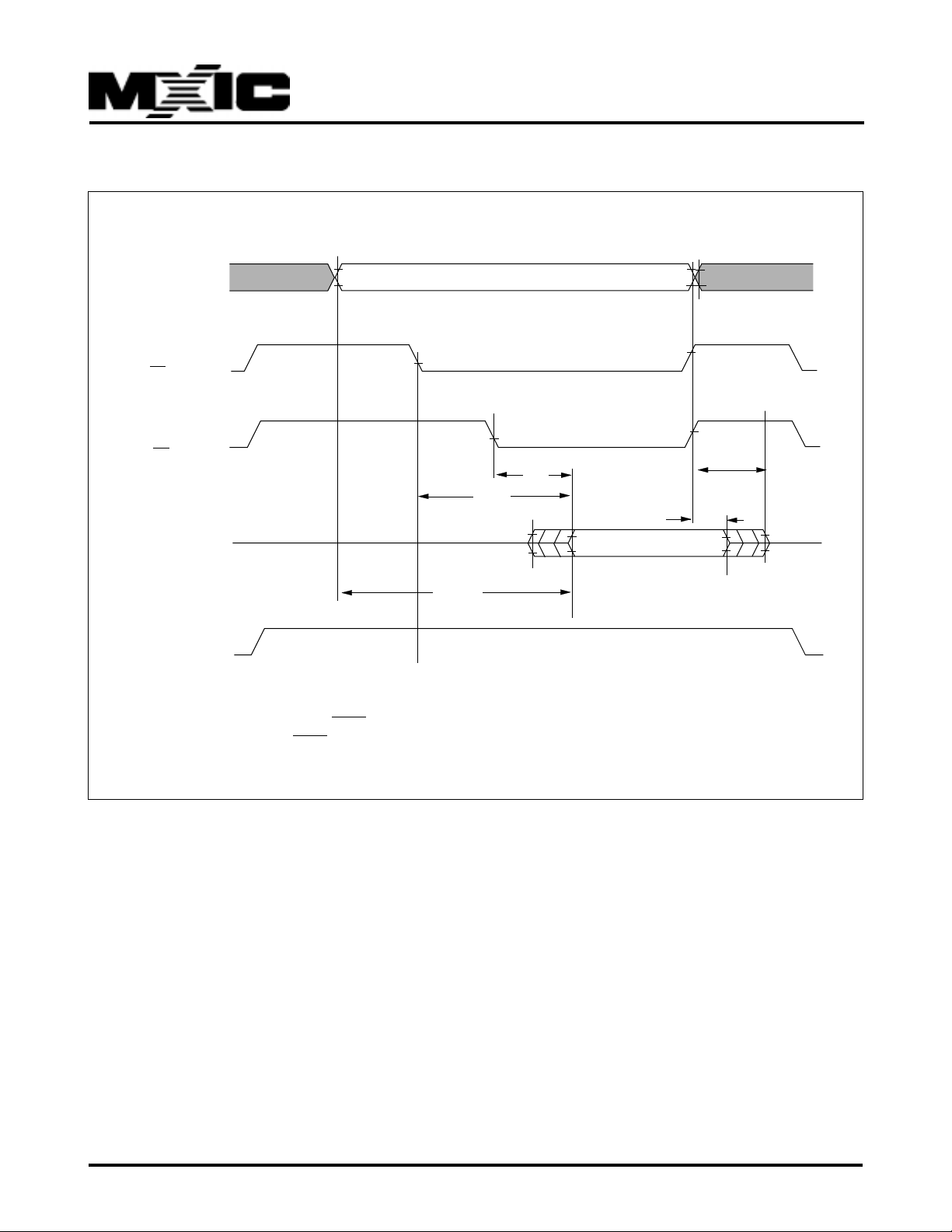
Figure 1. READ TIMING WAVEFORMS
MX27C1610
ADDRESSES
CE
OE
DATA OUT
VCC
Vcc
VIH
VIL
VIH
VIL
VIH
VIL
VOH
VOL
5.0V
GND
Power-up
HIGH Z
Standby
Device and
address selection
Outputs Enabled
ADDRESSES STABLE
tCE
tACC
tOE
Data valid
Data out valid
Standby
tOH
tDF
Vcc
Power-down
HIGH Z
NOTE:
1.For real world application, BYTE/VPP pin should be either static high(word mode) or static low(byte mode);
dynamic switching of BYTE/VPP pin is not recommended.
P/N:PM0593
REV. 1.3, APR. 26, 2000
11
Page 12
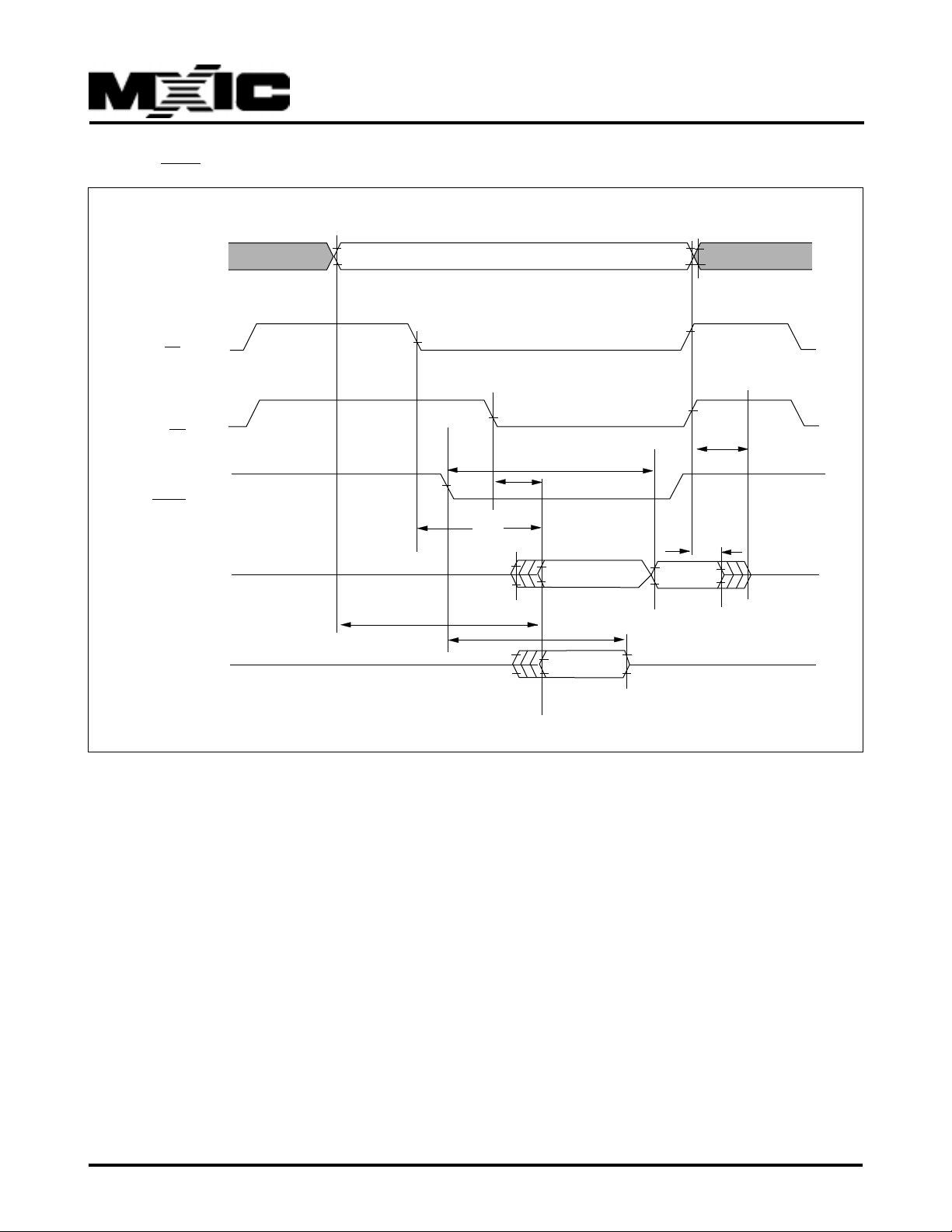
Figure 2. BYTE/VPP TIMING WAVEFORMS
MX27C1610
ADDRESSES
CE
OE
BYTE
DATA(Q0-Q7)
DATA(Q8-Q15)
VIH
VIL
VIH
VIL
VIH
VIL
VIH
VIL
VOH
VOL
VOH
VOL
HIGH Z
HIGH Z
ADDRESSES STABLE
tACC
tCE
tOE
tBACC
tBHZ
Data Output
Data Output
tOH
Data Output
tDF
HIGH Z
HIGH Z
P/N:PM0593
REV. 1.3, APR. 26, 2000
12
Page 13
MX27C1610
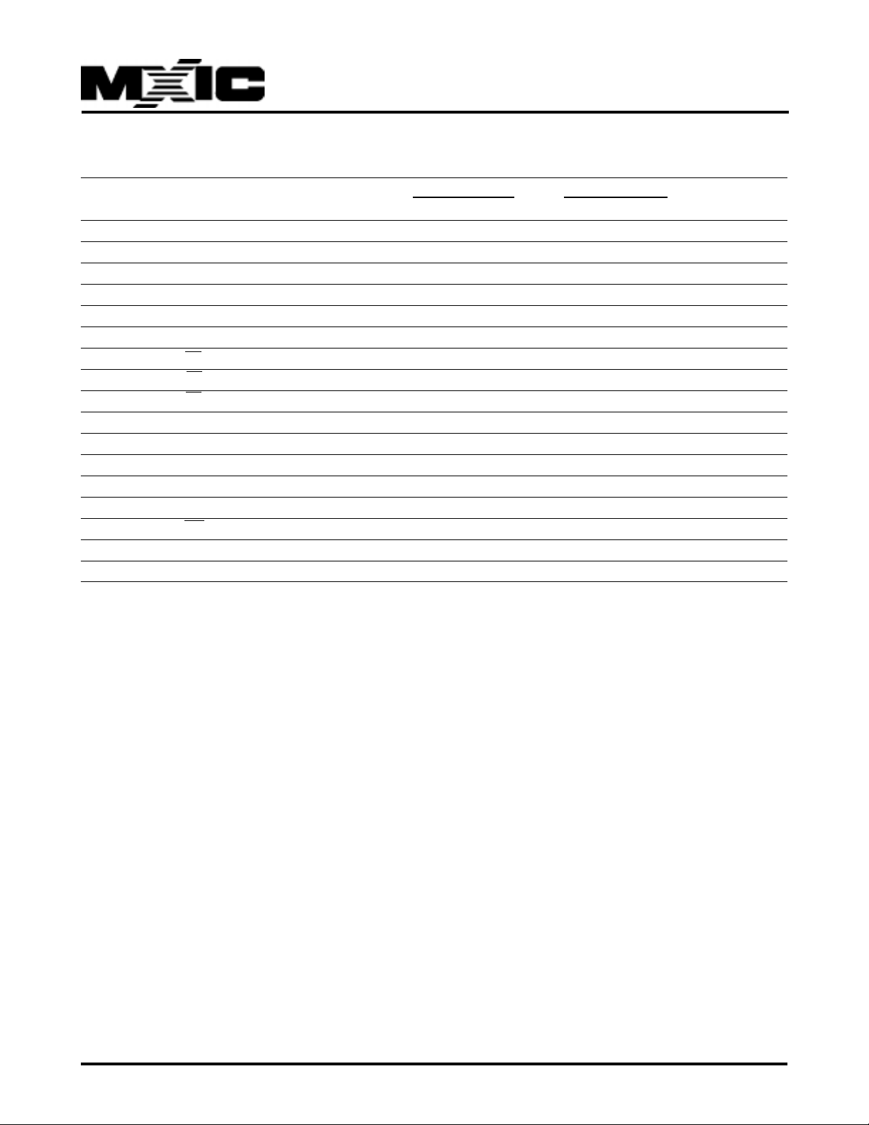
AC CHARACTERISTICS --- PROGRAM OPERATIONS
27C1610-10 27C1610-12
SYMBOL DESCRIPTION MIN. MAX. MIN. MAX. UNIT
tWC Write Cycle Time 100 120 ns
tAS Address Setup Time 0 0 ns
tAH Address Hold Time 50 60 ns
tDS Data Setup Time 50 60 ns
tDH Data Hold Time 0 0 ns
tOES Output Enable Setup Time 0 0 ns
tCES CE Setup Time 0 0 ns
tCS CE Setup Time 0 0 ns
tCH CE Hold Time 0 0 ns
tWP Write Pulse Width 50 60 ns
tWPH Write Pulse Width High 30 50 ns
tBALC Word Address Load Cycle 0.3 30 0.3 30 us
tBAL Word Address Load Time 100 100 us
tSRA Status Register Access Time 70 90 ns
tCESR CE Setup before S.R. Read 70 70 ns
tVCS VCC Setup Time 50 50 us
tRA W Read Operation Set Up Time After Write 20 20 us
P/N:PM0593
REV. 1.3, APR. 26, 2000
13
Page 14
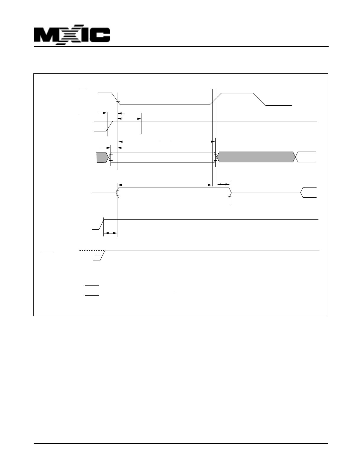
Figure 3. COMMAND WRITE TIMING WA VEFORMS
CE
tOES
tCS
OE
MX27C1610
ADDRESSES
BYTE/VPP
tAH
VALID
tDS
tDH
DIN
DATA
tAS
HIGH Z
(Q0~Q15)
10V
VCC
VIH
tVCS
VIL
NOTE:
1.BYTE/VPP pin should be static at 10V+0.5V during Write operation.
2.BYTE/VPP pin should be static at TTL, or CMOS level, during Read operation.
P/N:PM0593
REV. 1.3, APR. 26, 2000
14
Page 15
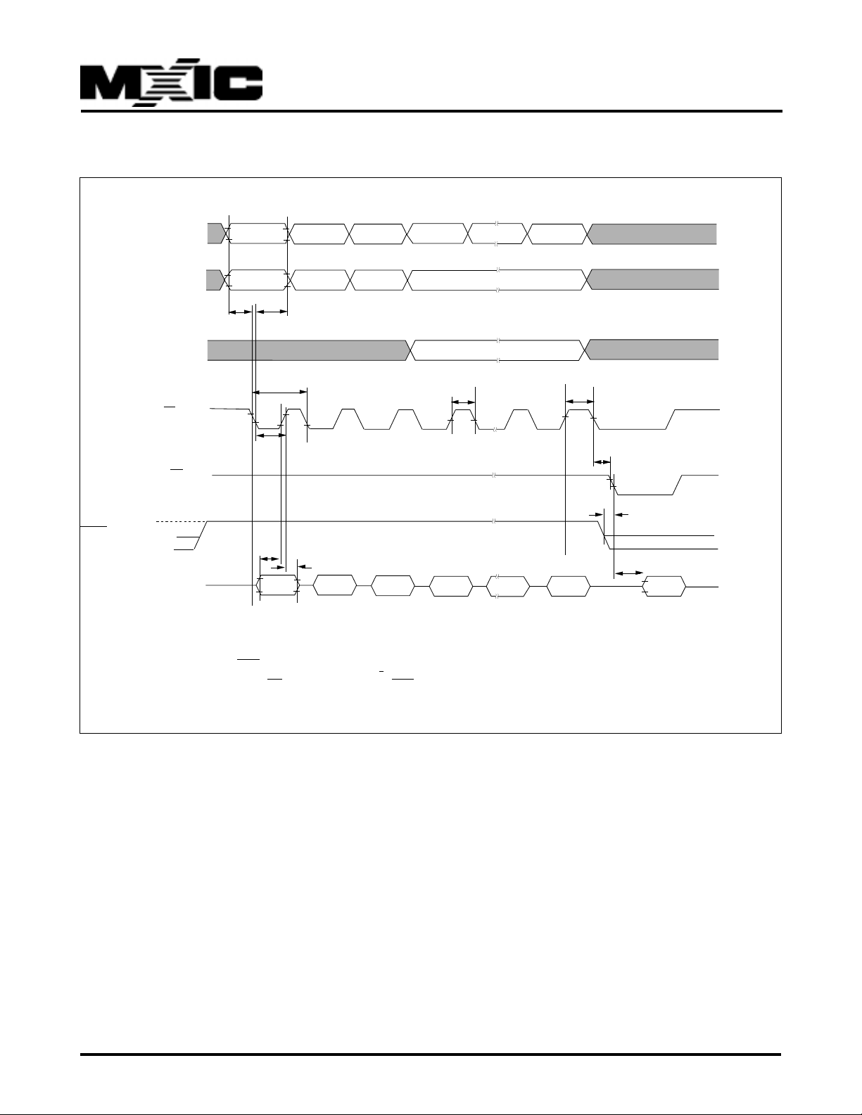
Figure 4. AUTOMATIC PAGE PROGRAM TIMING WAVEFORMS
MX27C1610
BYTE/VPP
A0~A5
A6~A14
A15~A19
10V
Q0~Q15
VIH
VIL
DATA
CE
OE
55H
55H
tAS
tAH
tWC
tWP
tDS
AAH 55H
tDH
AAH
2AH
55H
55H
Word offset
Address
Page Address
Last Word
offset Address
Page Address
tBALC
A0H SRD
Write
Data
tBAL
tCES
tRAW
tSRA
Last Write
Data
VIH
VIL
NOTE:
1.BYTE/VPP should be static at 10V+0.5V during page programming
2.Before OE going low to "read mode", BYTE/VPP must from VH(10V) to VIH or VIL
P/N:PM0593
REV. 1.3, APR. 26, 2000
15
Page 16
MX27C1610
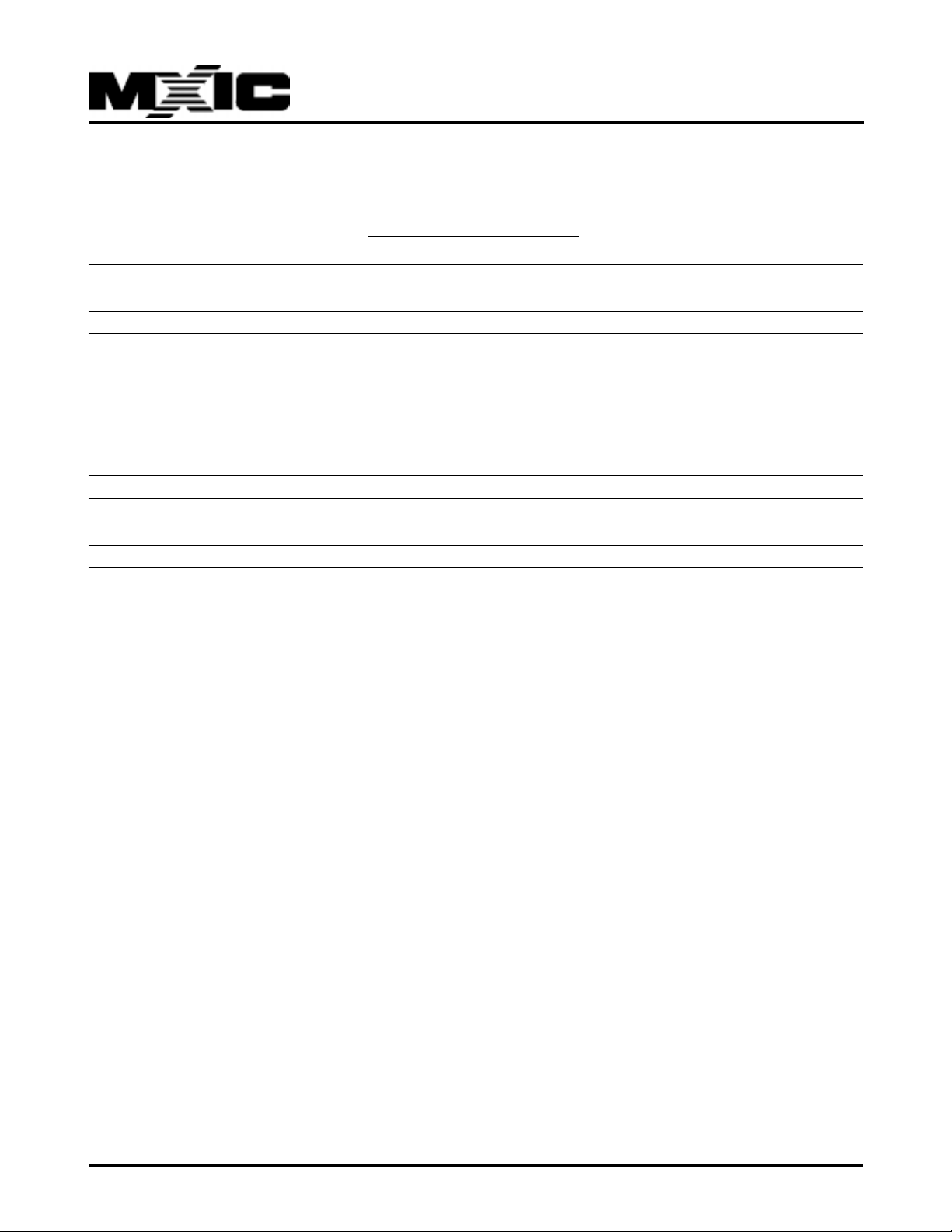
PROGRAMMING PERFORMANCE
LIMITS
PARAMETER MIN. TYP. MAX. UNITS
Page Programming Time 0.9 27 ms
Chip Programming Time 14 150 sec
Byte Program Time 7 us
LA TCHUP CHARA CTERISTICS
MIN. MAX.
Input Voltage with respect to GND on all pins except I/O pins -1.0V 13.5V
Input Voltage with respect to GND on all I/O pins -1.0V Vcc + 1.0V
Current -100mA +100mA
Includes all pins except Vcc. Test conditions: Vcc = 5.0V, one pin at a time.
P/N:PM0593
REV. 1.3, APR. 26, 2000
16
Page 17
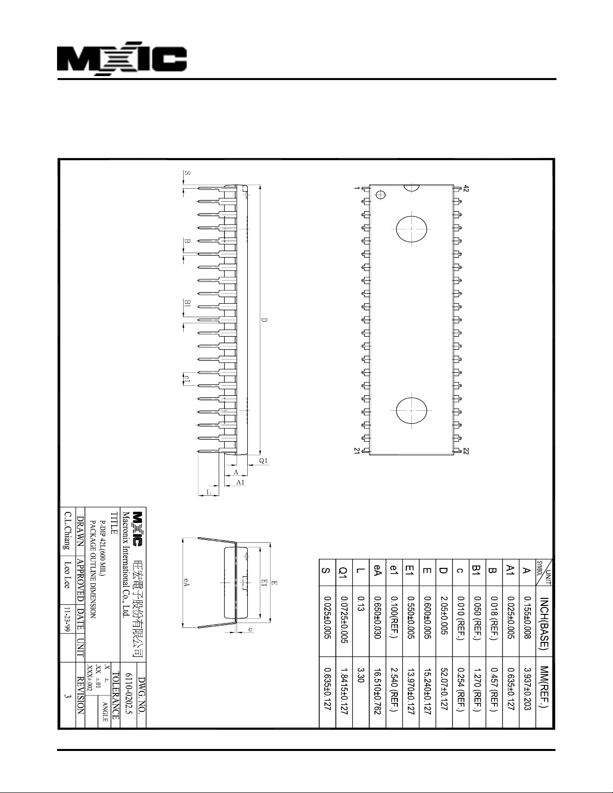
PACKAGE INFORMATION
42-PIN PLASTIC DIP (600 mil)
MX27C1610
P/N:PM0593
REV. 1.3, APR. 26, 2000
17
Page 18

MX27C1610
Revision History
Revision No. Description Page Date
1.3 Changed title from "Advanced Information" to "Preliminary" P1 APR/26/2000
P/N:PM0593
REV. 1.3, APR. 26, 2000
18
Page 19

MX27C1610
MACRONIX INTERNATIONAL CO., LTD.
HEADQUARTERS:
TEL:+886-3-578-6688
FAX:+886-3-563-2888
EUROPE OFFICE:
TEL:+32-2-456-8020
FAX:+32-2-456-8021
JAPAN OFFICE:
TEL:+81-44-246-9100
FAX:+81-44-246-9105
SINGAPORE OFFICE:
TEL:+65-348-8385
FAX:+65-348-8096
TAIPEI OFFICE:
TEL:+886-2-2509-3300
FAX:+886-2-2509-2200
MACRONIX AMERICA, INC.
TEL:+1-408-453-8088
FAX:+1-408-453-8488
CHICAGO OFFICE:
TEL:+1-847-963-1900
FAX:+1-847-963-1909
http : //www.macronix.com
MACRONIX INTERNATIONAL CO., LTD. reserves the right to change product and specifications without notice.
19
 Loading...