

Page 1
MX23L2000
INDEX
2M-BIT MASK ROM (8-BIT OUTPUT)
FEATURES
• Bit organization
- 256K x 8 (byte mode)
• Fast access time
- Random access: 150ns
• Current
- Operating: 20mA
- Standby: 20uA
• Supply voltage
- 2.7V ~ 3.6V
• Package
- 32 pin SOP (450 mil)
- 32 pin TSOP (8mm x 20mm)
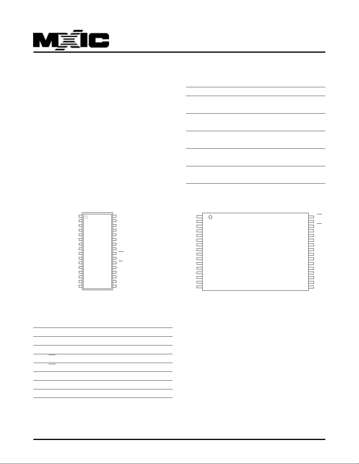
PIN CONFIGURATION
NC
A16
2
A15
3
A12
4
A7
5
A6
6
A5
7
A4
8
A3
9
A2
10
11
12
13
14
15
16
MX23L2000
VSS
A1
A0
D0
D1
D2
ORDER INFORMATION
Part No. Access Time Pac kage
MX23L2000MI-15 150ns 32 pin SOP
(Industrial)
MX23L2000MI-20 200ns 32 pin SOP
(Industrial)
MX23L2000TI-15 150ns 32 pin TSOP
(Industrial)
MX23L2000TI-20 200ns 32 pin TSOP
(Industrial)
MX23L2000TI-50 500ns 32 pin TSOP
(Industrial)
32 TSOP32 SOP
VCC
32
NC
31
A17
30
A14
29
A13
28
A8
27
A9
26
A11
25
OE
24
A10
23
CE
22
D7
21
D6
10
D5
19
D4
18
D3
17
VCC
A11
A13
A14
A17
NC
NC
A16
A15
A12
1
2
A9
3
A8
4
5
6
7
8
9
10
11
12
13
A7
14
A6
15
A5
16
A4
MX23L2000
32
OE
31
A10
30
CE
29
D7
28
D6
27
D5
26
D4
25
D3
24
VSS
23
D2
22
D1
21
D0
20
A0
19
A1
18
A2
17
A3
PIN DESCRIPTION
Symbol Pin Function
A0~A17 Address Inputs
D0~D7 Data Outputs
CE/CE Chip Enable Input
OE/OE Output Enable Input
VCC Po wer Supply Pin
VSS Ground Pin
NC No Connection
P/N:PM0337
REV. 2.4, FEB. 01, 1999
1
Page 2
MX23L2000
INDEX
ABSOLUTE MAXIMUM RATINGS
Item Symbol Ratings
Voltage on any Pin Relative to VSS VIN -0.3V to 3.9V
Ambient Operating Temperature Topr -40°C to 85°C
Storage Temperature Tstg -65°C to 125°C
DC CHARACTERISTICS (Ta = -40°C ~ 85°C, VCC = 2.7V ~ 3.6V)
Item Symbol MIN. MAX. Conditions
Output High Voltage V OH VCC-0.2V - IOH = -0.4mA
Output Low Voltage VOL - 0.2V IOL = 1.6mA
Input High Voltage VIH 2.0V VCC+0.3V
Input Low Voltage VIL -0.3V 0.4V
Input Leakage Current ILI - 5uA VIN = 0 to VCC
Output Leakage Current ILO - 5uA VOUT = 0 to VCC
Operating Current ICC1 - 20mA VCC=3V, f = 5MHz
Standby Current (TTL) ISTB1 - 1mA CE = VIH
Standby Current (CMOS) ISTB2 - 20uA CE >VCC - 0.2V
Input Capacitance CIN - 10pF T a=25°C, f=1MHz, VIN=0V
Output Capacitance COUT - 10pF Ta=25°C, f=1MHz, VOUT=0V
AC CHARACTERISTICS (Ta = -40°C ~ 85°C, VCC = 2.7V ~ 3.6V)
Item Symbol 23L2000-15 23L2000-20 23L2000-50
MIN. MAX. MIN. MAX. MIN. MAX.
Read Cycle Time tRC 150ns - 200ns - 500ns Address Access Time tAA - 150ns - 200ns - 500ns
Chip Enable Access Time tACE - 150ns - 200ns - 500ns
Output Enable Time tOE - 70ns - 100ns - 230ns
Output Hold After Address tOH 0n s - 0ns - 0ns Output High Z Delay tHZ - 20ns - 20ns - 20ns
Note :Output high-impedance delay (tHZ) is measured
from OE or CE going high, and this parameter guaranteed by design over the full voltage and temperature
operating range - not tested.
P/N:PM0337
REV. 2.4, FEB. 01, 1999
2
Page 3

AC T est Conditions
INDEX
Input Pulse Levels 0.4V~2.4V
Input Rise and Fall Times 10ns
Input Timing Level 1.4V
Output Timing Level 1.4V
Output Load See Figure
TIMING DIAGRAM
RANDOM READ
MX23L2000
IOH (load)=-0.4mA
DOUT
IOL (load)=1.6mA
Note:No output loading is present in tester load board.
Active loading is used and under software programming control.
Output loading capacitance includes load board's and all stray capacitance.
C<100pF
ADD
CE
OE
DATA
Note : CE, OE are enable.
ADD
tACE
tOE
VALLID
tAA
ADD
tRC
VALLID
tOH
ADD
tHZ
VALLID
P/N:PM0337
REV. 2.4, FEB. 01, 1999
3
Page 4
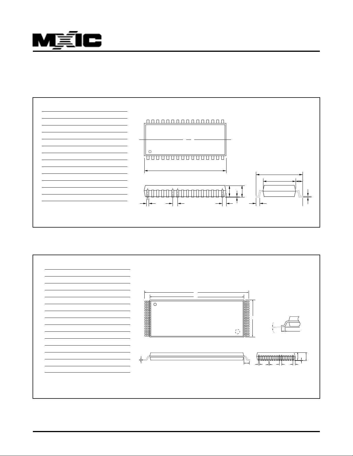
PACKAGE INFORMATION
INDEX
32-PIN PLASTIC SOP (450 mil)
MX23L2000
ITEM MILLIMETERS INCHES
A 20.95 max. .825 max.
B 1.00 [REF] .039 [REF]
C 1.27 [TP] .050 [TP]
D .40 [Typ.] .016 [Typ.]
E .05 min. .002 min.
F 3.05 max. .120 max.
G 2.69±.13 .106±.005
H 14.12±.25 .556±.010
I 11.30±.13 .445±.005
J 1.42 .056
K .20 [Typ.] .008 [Typ.]
L .79 .031
NOTE: Each lead centerline is located within .25 mm[.01
inch] of its true position [TP] at maximum material condition.
32-PIN PLASTIC TSOP
ITEM MILLIMETERS INCHES
A 20.0±.20 .078±.006
B 18.40±.10 .724±.004
C 8.20 max. .323 max.
D .15 [Typ.] .006 [Typ.]
E .80 [Typ.] .031 [Typ.]
F .20±.10 .008±.004
G .30±.10 .012±.004
H .50 [Typ.] .020 [Typ.]
I .45 max. .018 max.
J 0 ~ .20 0 ~ .008
K 1.00±.10 .039±.004
L 1.27 max. .050 max.
M .50 .020
N0 ~ 5° .500
NOTE: Each lead centerline is located within .25 mm[.01
inch] of its true position [TP] at maximum material condition.
1732
116
A
GF
DC B
A
B
D
E
L
C
N
E
F
G
H
JI
K
M
KL
J
I
H
P/N:PM0337
REV. 2.4, FEB. 01, 1999
4
Page 5

MX23L2000
INDEX
REVISION HISTORY
REVISION DESCRIPTION PAGE D ATE
2.3 AC CHARACTERISTICS:To add 500ns speed grade. P2 NOV/05/1998
AC TEST CHARACTERISTICS: P3
The output timing level is changed as1.4V instead of 0.8V and 2.0V
2.4 AC Characteristics: tOH 10ns --> 0ns P3 FEB/01/1999
P/N:PM0337
REV. 2.4, FEB. 01, 1999
5
Page 6

MX23L2000
INDEX
MACRONIX INTERNATIONAL CO., LTD.
HEADQUARTERS:
TEL:+886-3-578-8888
FAX:+886-3-578-8887
EUROPE OFFICE:
TEL:+32-2-456-8020
FAX:+32-2-456-8021
JAPAN OFFICE:
TEL:+81-44-246-9100
FAX:+81-44-246-9105
SINGAPORE OFFICE:
TEL:+65-747-2309
FAX:+65-748-4090
TAIPEI OFFICE:
TEL:+886-3-509-3300
FAX:+886-3-509-2200
MACRONIX AMERICA, INC.
TEL:+1-408-453-8088
FAX:+1-408-453-8488
CHICAGO OFFICE:
TEL:+1-847-963-1900
FAX:+1-847-963-1909
http : //www.macronix.com
MACRONIX INTERNATIONAL CO., LTD. reserves the rignt to change product and specifications without notice.
6
 Loading...