

Page 1
DATA BULLETIN
MX128
*Electronics Communications Privacy Act (Title 18, US Code 2510 et seq.)
©1998 MX-COM Inc. www.mxcom.com Tel: 800 638-5577 336 744-5050 Fax: 336 744-5054 Doc. # 20480101.010
4800 Bethania Station Road, Winston-Salem, NC 27105-1201 USA All trademarks and service marks are held by their respective companies.
Cordless Telephone Scrambler
Features Applications
Full-Duplex Audio Processing
On-Chip Filters
Carrier Rejection >55dB
Uses IF (10.24 MHz) Clock
Requires No Extra Crystal
Excellent Audio Quality
Low Voltage 3.3V/5.0V Operation
ECPA* Qualified Voice Protection
Battery Powered Portability
Cordless Telephones
Wireless PBXs
+
+
RX Path
TX Path
V
V
BIAS
BIAS
Inversion
Carrier
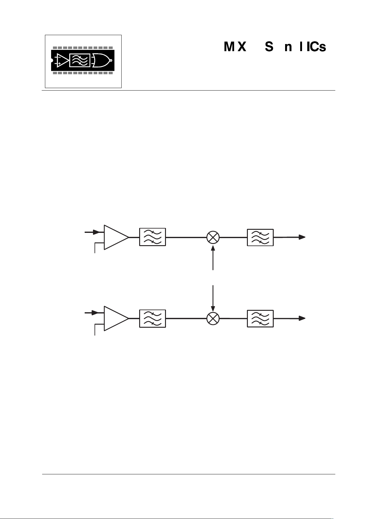
The MX128 is a full-duplex frequency inversion scrambler designed to provide secure conversations for 46/49
MHz cordless telephone users. The RX and TX audio paths consist of the following:
1. A switched-capacitor balanced modulator with high baseband and carrier rejection.
2. A 3.3 kHz inversion carrier (injection tone).
3. A 3100 Hz lowpass filter.
4. Input op-amps with externally adjustable gain.
The MX128 uses mixed signal CMOS switched-capacitor filter technology and operates from a single supply
in the range of 3.0V to 5.5V. The inversion carrier's frequency and filter switching clock are generated on-chip
using an external 10.24 MHz or 3.58/3.6864 MHz crystal or clock input (selectable).
The MX128 is available in the following package styles: 16-pin SOIC (MX128DW) and 16-pin PDIP
(MX128P).
Page 2

Cordless Telephone Scrambler 2 MX128
©1998 MX-COM Inc. www.mxcom.com Tel: 800 638-5577 336 744-5050 Fax: 336 744-5054 Doc. # 20480101.010
4800 Bethania Station Road, Winston-Salem, NC 27105-1201 USA All trademarks and service marks are held by their respective companies.
CONTENTS
Section Page
1. Block Diagram ..........................................................................................................3
2. Signal List .................................................................................................................4
3. External Components ..............................................................................................5
4. Application................................................................................................................6
4.1 Application Notes.................................................................................................................... 6
5. Performance Specification......................................................................................7
5.1 Electrical Performance ........................................................................................................... 7
5.2 Packaging............................................................................................................................. 10
MX•COM, Inc. reserves the right to change specifications at any time and without notice.
Page 3
Cordless Telephone Scrambler 3 MX128
©1998 MX-COM Inc. www.mxcom.com Tel: 800 638-5577 336 744-5050 Fax: 336 744-5054 Doc. # 20480101.010
4800 Bethania Station Road, Winston-Salem, NC 27105-1201 USA All trademarks and service marks are held by their respective companies.
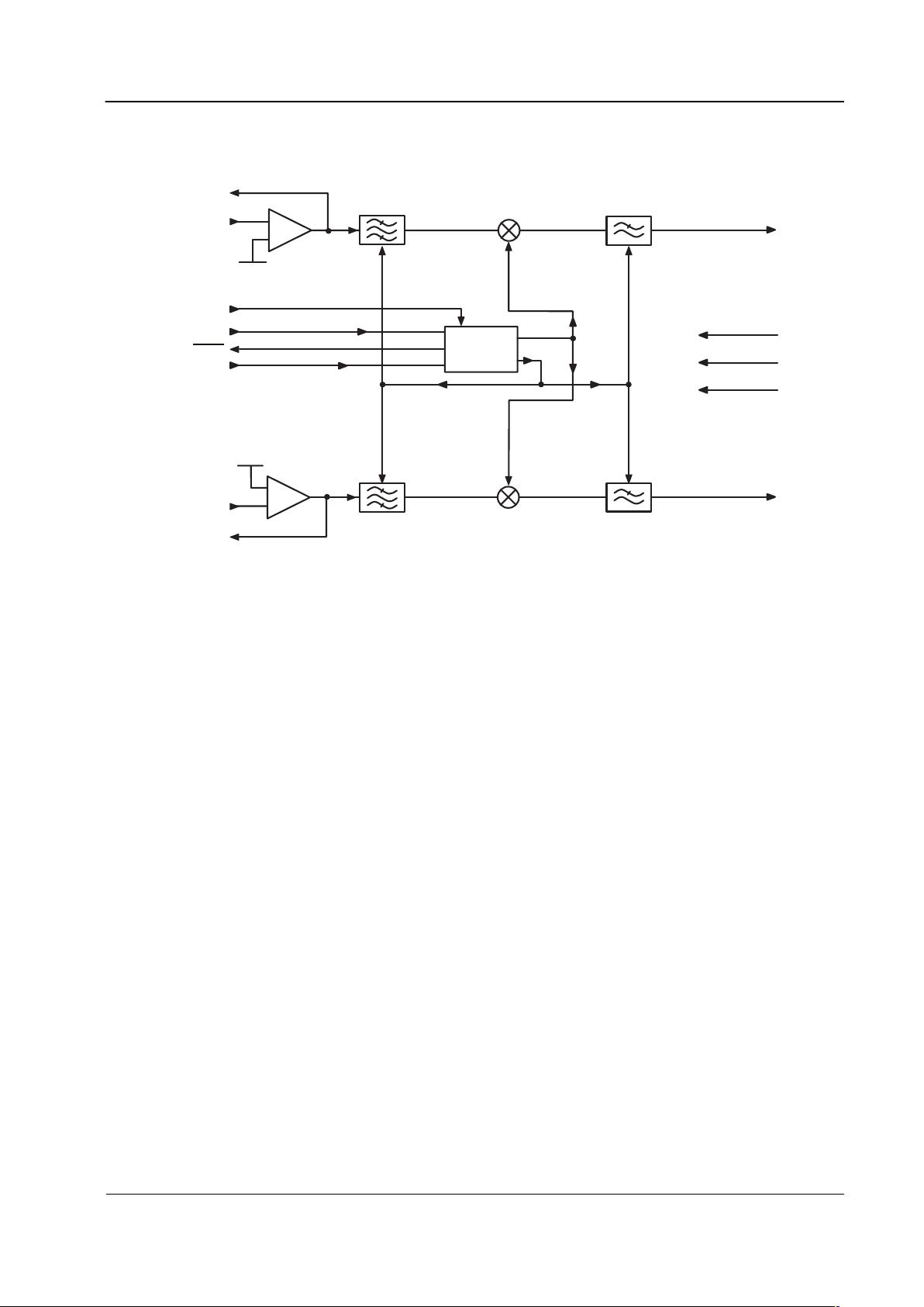
1. Block Diagram
+
-
+
CLOCKS
AND
LOGIC
RX GAIN AMP
OUT
RXIN
12
11
2
1
15
14
6
5
4
8
9
16
13
V
BIAS
V
DD
V/2
DD
V
SS
XT AL/CLOCK
CLR
10.24/3.58 MHz
CLOCK SELECT
XT AL
TXIN
TX GAIN AMP
OUT
RX CHANNEL
TX CHANNEL
212 kHz
3.3 kHz
RXOUT
TXOUT
0V
V
BIAS
V
BIAS
Figure 1: Device Block Diagram
Page 4

Cordless Telephone Scrambler 4 MX128
©1998 MX-COM Inc. www.mxcom.com Tel: 800 638-5577 336 744-5050 Fax: 336 744-5054 Doc. # 20480101.010
4800 Bethania Station Road, Winston-Salem, NC 27105-1201 USA All trademarks and service marks are held by their respective companies.
2. Signal List
Pin No. Signal Type Description
1
Xtal
output
This is the output of the clock oscillator inverter
2 Xtal/Clock input A 10.24 MHz, 3.58/3.6864 MHz, or an externally derived clock
signal is injected at this pin. See Figure 3
4 TXOUT output This is the analog output of the transmit channel. It is internally
biased at V
DD
/2
5 TX Gain Ampout output This is the output pin of the transmit channel gain adjusting op-
amp. See Figure 4 for gain setting components
6 TXIN input This is the analog signal input to the transmit channel. This input
is to a gain adjusting op-amp whose gain is set by internal
components. See Figure 4.
8VSSpower Negative supply (GND)
9V
BIAS
output This is an internally generated bias voltage output (VDD/2)
11 RXIN input This is the analog signal input to the receive channel. This input is
to a gain adjusting op-amp whose gain is set by internal
components. See Figure 4.
12 RX Gain Ampout output This is the output pin of the receive channel gain adjusting op-
amp. See Figure 4 for gain setting components
13 RXOUT output This is the analog output of the receive channel. It is internally
biased at V
DD
/2
14 CLR A logic 1 on this input selects the invert mode. A logic 0 selects
the clear (not inverted) mode
15 Clock Select Selects either 10.24 or 3.58/3.6864 MHz clock frequency. A logic
“1” selects 10.24 MHz, and a logic “0” selects 3.58/3.6864 MHz.
This input is internally pulled high
16 V
DD
power Positive supply of 3.0V to 5.5 V
3, 7, 10 N/C No internal connections
Page 5

Cordless Telephone Scrambler 5 MX128
©1998 MX-COM Inc. www.mxcom.com Tel: 800 638-5577 336 744-5050 Fax: 336 744-5054 Doc. # 20480101.010
4800 Bethania Station Road, Winston-Salem, NC 27105-1201 USA All trademarks and service marks are held by their respective companies.
3. External Components
MX128
INSET
SEE INSET
BELOW
SEE INSET
BELOW
1
2
3
4
5
6
7
8
1
2
3
4
5
6
7
8
16
15
14
13
12
11
10
9
16
15
14
13
12
11
10
9
XTAL
XTAL/CLOCK
N/C
TXOUT
TX GAIN AMP OUT
TXIN
N/C
XTAL
XTAL/CLOCK
N/C
TXOUT
TX GAIN AMP OUT
TXIN
N/C
R
X
C
C
C
SS
1
1
2
3
1
DD
BIAS
V
DD
V
CLK SEL
CLR
RXOUT
RX GAIN AMP OUT
RXIN
N/C
V
V
CLK SEL
CLR
RXOUT
RX GAIN AMP OUT
RXIN
N/C
V
XTAL/CLOCK
XTAL
1
2
MX128
SEE
FIG. 4
SEE
FIG. 4
SEE
FIG. 4
SEE
FIG. 4
}
}
V
10.24 MHz 3.58/3.6864 MHz
R1
1.0M
10%
R1
1.0M
10%
C1 0.47µF
20%
C1 0.47µF
20%
C2 22.0pF
20%
C2 33.0pF
20%
C3 22.0pF
20%
C3 47.0pF
20%
X1 10.24 MHz X1 Note 1 3.58/3.6864 MHz
Figure 2: Recommended External Components
External Components Note:
1. For best results, a crystal oscillator should drive the clock inverter input with signal levels of at least
40% of V
DD
peak - peak. Tuning fork crystals generally cannot meet this requirement. To obtain
crystal oscillator design assistance, consult your crystal manufacturer.
Page 6

Cordless Telephone Scrambler 6 MX128
©1998 MX-COM Inc. www.mxcom.com Tel: 800 638-5577 336 744-5050 Fax: 336 744-5054 Doc. # 20480101.010
4800 Bethania Station Road, Winston-Salem, NC 27105-1201 USA All trademarks and service marks are held by their respective companies.
4. Application
12
120pF
100k
100k
100k
100k
100k
100k
RXIN
RXOUT
11
13
.1uF
.1uF
150pF
150pF
150pF
150pF
5
120pF
100k
100k
TXIN
TXOUT
6
4
.1uF
.1uF
RF AMP
RF
AMP
AF
AMP
AF AMP
HYBRID
TRANSFORMER
TELEPHONE
LINE
DE-EMP
PREEMP
CODE
DETECT
CODE
ENCODE
MODULATOR
FM
DETECTOR
IF
AMP
P
m
BASE
12
120pF
100k
100k
RXIN
RXOUT
11
13
.1uF
.1uF
5
120pF
100k
100k
TXIN
TXOUT
6
4
.1uF
.1uF
RF AMP
RF
AMP
AF
AMP
MIC.
AF AMP
SPKR
DE-EMP
PREEMP
CODE
DETECT
CODE
ENCODE
MODULATOR
KEYPAD
FM
DETECTOR
IF
AMP
DTMF
Generation
P
PORTABLE
MX128
MX128
Note: Components shown set a gain of 0dB.
Figure 3: Block Diagram of a Typical Application of the MX128 (Cordless Phone)
4.1 Application Notes
Formulas for calculating the carrier frequency, upper cutoff frequency and lower cutoff frequency with clock
select pin high are as follows:
Carrier Frequency = (3.2995kHz / 10.24MHz) * XTAL frequency
Upper Cutoff Frequency = (2.800kHz / 10.24MHz) * XTAL frequency
Lower Cutoff Frequency = (400Hz / 10.24MHz) * XTAL frequency
Formulas for calculating the carrier frequency, upper cutoff frequency and lower cutoff frequency with clock
select pin low are as follows:
Carrier Frequency = (3.2995kHz / 3.415MHz) * XTAL frequency
Upper Cutoff Frequency = (2.800kHz / 3.415MHz) * XTAL frequency
Lower Cutoff Frequency = (400Hz / 3.415MHz) * XTAL frequency
Page 7

Cordless Telephone Scrambler 7 MX128
©1998 MX-COM Inc. www.mxcom.com Tel: 800 638-5577 336 744-5050 Fax: 336 744-5054 Doc. # 20480101.010
4800 Bethania Station Road, Winston-Salem, NC 27105-1201 USA All trademarks and service marks are held by their respective companies.
5. Performance Specification
5.1 Electrical Performance
Absolute Maximum Ratings
Exceeding these maximum ratings can result in damage to the device.
General Min. Max. Units
Supply Voltage (VDD - VSS) -0.3 7.0 V
Voltage on any pin to V
SS
-0.3 VDD + 0.3 V
Current
V
DD
-30 30 mA
V
SS
-30 30 mA
Any other pin -20 20 mA
P/DW Packages
Total Allowable Power Dissipation at T
AMB
= 25°C 800 mW max.
Derating above 25°C 10 mW/°C above 25°C
Operating Temperature -40 85 °C
Storage Temperature -55 125 °C
Operating Limits
Correct operation of the device outside these limits is not implied.
Notes Min. Max. Units
Supply (VDD - VSS)3.05.5V
Operating Temperature -40 85 °C
Clock Frequency 10.24 MHz
Page 8

Cordless Telephone Scrambler 8 MX128
©1998 MX-COM Inc. www.mxcom.com Tel: 800 638-5577 336 744-5050 Fax: 336 744-5054 Doc. # 20480101.010
4800 Bethania Station Road, Winston-Salem, NC 27105-1201 USA All trademarks and service marks are held by their respective companies.
Operating Characteristics
For the following conditions unless otherwise specified:
V
DD
= 3.3V at T
AMB
= 25°C
Clock Frequency = 10.24MHz
Audio Level 0dB ref. @ 1kHz = (V
DD
-1) x 150mV
RMS
e.g. VDD = 3.3V 0dB = 345mV
RMS.
Notes Min. Typ. Max Units
Static Values
Supply Current 2.0 3.0 mA
Input Impedance
Digital 2 100
k
Amplifiers 2 1.0 10.0
M
Output Impedance (RXOUT, TXOUT) 1.0
k
Input Logic 1 Voltage 1 70% V
DD
Input Logic 0 Voltage 1 30% V
DD
Dynamic Values
Analog Signal Input Levels -16.0 3 dB
Analog Output Noise 4 2.5 5.0 mV
RMS
Clear Mode
Passband -3dB Cutoff Frequencies
Low 300 Hz
High 3000 Hz
Passband Ripple (300-3000Hz)
RX Channel 0 3.6 dB
TX Channel 0 2.9 dB
Passband Ripple (500-2750Hz)
RX Channel 0 2.2 dB
TX Channel 0 2.0 dB
Filter Attenuation at 3.3 kHz
RX Channel 30 dB
TX Channel 30 dB
Filter Attenuation at 3.6 kHz
RX Channel 45 dB
TX Channel 45 dB
Passband Gain (@1kHz ref.)
RX Channel -1.5 0.5 dB
TX Channel -1.5 0.5 dB
Switched-Capacitor Filter Sampling 211.066 kHz
Carrier Frequency 3298 Hz
Invert Mode Combined TX and RX Response
Passband -3dB Cutoff Frequencies
Low 400 Hz
High 2800 Hz
Passband Gain -3 0.5 dB
Distortion (@1kHz) 3 1.75 2.75 %
Passband Gain (@1kHz ref.) 5 -2.5 -1.5 0 dB
Low Frequency Roll-off (<200 Hz) 12 dB/octave
Page 9

Cordless Telephone Scrambler 9 MX128
©1998 MX-COM Inc. www.mxcom.com Tel: 800 638-5577 336 744-5050 Fax: 336 744-5054 Doc. # 20480101.010
4800 Bethania Station Road, Winston-Salem, NC 27105-1201 USA All trademarks and service marks are held by their respective companies.
Notes Min. Typ. Max Units
Invert Mode Single Channel Response
Unwanted Modulation Products 3
RX Channel -40 dB
TX Channel -40 dB
Carrier Breakthrough 3
RX Channel -55 dB
TX Channel -55 dB
Baseband Breakthrough 3
RX Channel -40 dB
TX Channel -40 dB
Operating Characteristics Notes:
1. Batch sampled only
2. By characterization only
3. Measured with Input Level 0dB
4. Short circuit RX or TX input, measure noise at corresponding analog output, in 30KHz bandwidth
5. Op Amp gain 0dB
6. Clear mode only
Page 10

Cordless Telephone Scrambler 10 MX128
©1998 MX-COM Inc. www.mxcom.com Tel: 800 638-5577 336 744-5050 Fax: 336 744-5054 Doc. # 20480101.010
4800 Bethania Station Road, Winston-Salem, NC 27105-1201 USA All trademarks and service marks are held by their respective companies.
5.2 Packaging
PIN 1
A
B
ALTERNATIVE
PIN
LOCATION
MARKING
X
P
J
Y
C
K
H
E
L
T
W
Z
NOTE: All dimensions in inches(mm.)
Angles are in degrees
PackageTolerances
A
B
C
E
H
TYP.
MAX.MIN.
DIM.
J
P
X
W
T
Y
K
L
0.105 (2.67)0.093 (2.36)
0.419 (10.64)
45°
7°
0° 10°
0.050 (1.27)
0.041 (1.04)
0.413 (10.49)
0.299 (7.59)
0.050 (1.27)
0.016 (0.41)
0.390 (9.90)
0.020 (0.51)0.003 (0.08)
0.009 (0.23) 0.0125 (0.32)
0.013 (0.33) 0.020 (0.51)
0.395 (10.03)
0.286 (7.26)
Z
5°
5°
Figure 4: 16-pin SOIC Mechanical Outline: Order as part no. MX128DW
PackageTolerances
NOTE: All dimensions in inches(mm.)
Angles are in degrees
TYP. MAX.MIN.
A
B
C
E
E1
H
DIM.
J
J1
P
Y
T
K
L
0.200 (5.06)
0.262 (6.63)
0.390 (9.91).
7°
0.150 (3.81)
0.810 (20.57)
0.135 (3.43)
0.100 (2.54)
0.121 (3.07)
0.300 (7.62)
0.290 (7.37) 0.325 (8.26)
0.015 (0.38) 0.070 (1.77)
0.008 (0.20) 0.015 (0.38)
0.014 (0.35) 0.023 (0.58)
0.040 (1.02) 0.065 (1.65)
0.056 (1.42) 0.064 (1.63)
0.740 (18.80)
0.240 (6.10)
B
A
PIN 1
E
Y
E1
T
K
H
J1
J
C
P
L
Figure 5: 16-pin PDIP Mechanical Outline: Order as part no. MX128P
 Loading...