

Page 1
DATA BULLETIN
MX105A
FEATURES
•
Operates in High Noise Conditions
•
36 dB Signal Input Range
• ≥
High Sensitivity
•
Low Power Operation 2.7 V to 5.5 V
•
Adjustable Bandwidth
•
Adjustable Frequency
•
C4
C2
C2
A
7
8
B
R2
4
Loop
Filter
-
+
2
Input Amp
-
+
Timing
Logic
Tone Detector
PRELIMINARY INFORMATION
APPLICATIONS
•
Single and Multitone System
•
Applications
Tone In
1
C5
V/2
DD
3
Detect
Filter
+
-
R3
16
V
DD
C6
C3
A
5
6
C3
B
11
R4
12
VCO
1513
14
MX105A
Detect Counter
9
10
Detect
C1
The MX105A is a monolithic CMOS tone detector for tone decoding in single and multitone signaling systems. Using
phase locked loop (PLL) decoding techniques, the MX105A recognizes tones in the presence of high noise levels and
strong adjacent channel tones. Detection frequency and bandwidth can each be independently adjusted. The design is
immune to high levels of harmonic and sub-harmonic noise. It also maintains excellent noise immunity and constant
bandwidth over a wide range of input signal levels.
The MX105A requires a voltage supply of 2.7V to 5.5V and is available in the following package styles: 16-pin SOIC
(MX105ADW), 16-pin PDIP (MX105AP), and 24-pin PLCC (MX105ALH).
© 1997 MX•COM, INC. www.mxcom.com Tele: 800 638 5577 910 744 5050 Fax: 910 744 5054 Doc.# 20480133.003
4800 Bethania Station Road, Winston-Salem, NC 27105-1201 USA All trademarks and service marks are held by their respective companies.
R1
B
C1
A
R
L
Out
Page 2

Tone Detector 2 MX105A PRELIMINARY INFORMATION
CONTENTS
Section..........................................................................................................................Page
1. Block Diagram ................................................................................................................3
2. Signal List .......................................................................................................................4
3. External Components ....................................................................................................5
4. General Description .......................................................................................................6
5. Application......................................................................................................................7
5.1 Method for Calculating External Component Values...............................................................7
5.2 Define f0..................................................................................................................................7
5.3 Calculate Minimum Usable Bandwidth....................................................................................7
5.4 Calculate The Recommended Operating Bandwidth..............................................................7
5.5 Select R4 for Operating BW....................................................................................................8
5.6 Calculate R2×C2A...................................................................................................................8
5.7 Define Maximum Allowed Response Time..............................................................................8
5.8 Calculate R3×C3A...................................................................................................................8
5.9 Calculate Maximum De-response Time..................................................................................9
5.10 Calculate Signal to Noise Performance...............................................................................10
5.11 Calculate C4 for 30° Phase Shift.........................................................................................10
6. Performance Specification ..........................................................................................11
6.1 Electrical Performance..........................................................................................................11
6.1.1 Absolute Maximum Ratings..........................................................................................................11
6.1.2 Operating Limits............................................................................................................................11
6.1.3 Operating Characteristics.............................................................................................................12
6.2 Packaging..............................................................................................................................13
MX•COM, Inc. reserves the right to change specifications at any time and without notice.
© 1997 MX•COM, INC. www.mxcom.com Tele: 800 638 5577 910 744 5050 Fax: 910 744 5054 Doc.# 20480133.003
4800 Bethania Station Road, Winston-Salem, NC 27105-1201 USA All trademarks and service marks are held by their respective companies.
Page 3
Tone Detector 3 MX105A PRELIMINARY INFORMATION
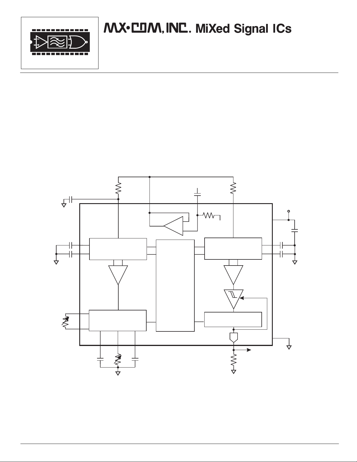
1. Block Diagram
R4
C4
C2
C2
R2
Tone In
R3
C5
V
C3
C3
DD
C6
A
B
4
2
Input Amp
-
+
A
7
8
B
11
12
Loop
Filter
-
VCO
1513
+
14
Timing
Logic
MX105A
1
V/2
DD
Detect Counter
3
Detect
Filter
+
-
9
16
5
6
10
Detect
C1
R1
B
C1
A
R
L
Out
Figure 1: Block Diagram
© 1997 MX•COM, INC. www.mxcom.com Tele: 800 638 5577 910 744 5050 Fax: 910 744 5054 Doc.# 20480133.003
4800 Bethania Station Road, Winston-Salem, NC 27105-1201 USA All trademarks and service marks are held by their respective companies.
Page 4

Tone Detector 4 MX105A PRELIMINARY INFORMATION
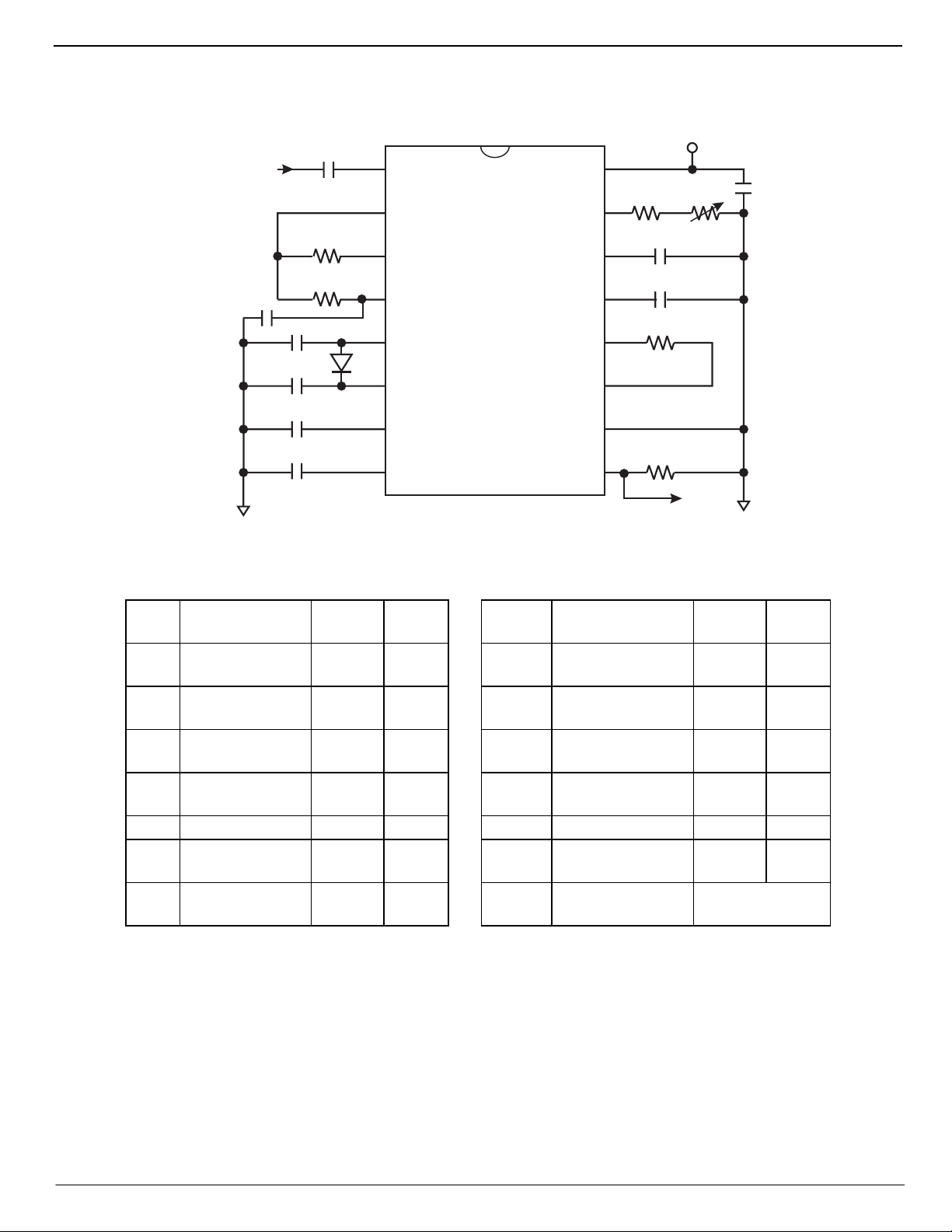
2. Signal List
Pin No. Pin No. Name Type Description
DW/P LH
1 1 INPUT AMP IN input AC couple to this input. Nominal input
impedance is 200 kΩ.
2 3 INPUT AMP OUT output
3 5 R3 input Detect filter resistor pin.
4 6 R2 input PLL loop filter resistor pin. For improved
57 C3
68 C3
710 C2
811 C2
A
B
A
B
output Detect filter capacitor pin A
output Detect filter capacitor pin B
output Loop filter capacitor pin A
output Loop filter capacitor pin B
9 13 DETECT OUT output PMOS open drain output - active on detect.
10 14 V
11 16 R4
12 17 R4
13 19 C1
14 20 C1
SS
A
B
B
A
power Ground.
input Bandwidth control resistor pin A
input Bandwidth control resistor pin B
output VCO capacitor B
output VCO capacitor A
15 22 R1 input VCO discharge resistor. When potentiometer
16 24 V
DD
power Power supply.
Nominal output impedance is 1 kΩ.
performance C4 may be chosen to provide 30°
of phase shift at the loop filter input.
tuning is required, a series resistor is
recommend to prevent possible shorting to
ground.
© 1997 MX•COM, INC. www.mxcom.com Tele: 800 638 5577 910 744 5050 Fax: 910 744 5054 Doc.# 20480133.003
4800 Bethania Station Road, Winston-Salem, NC 27105-1201 USA All trademarks and service marks are held by their respective companies.
Page 5
Tone Detector 5 MX105A PRELIMINARY INFORMATION
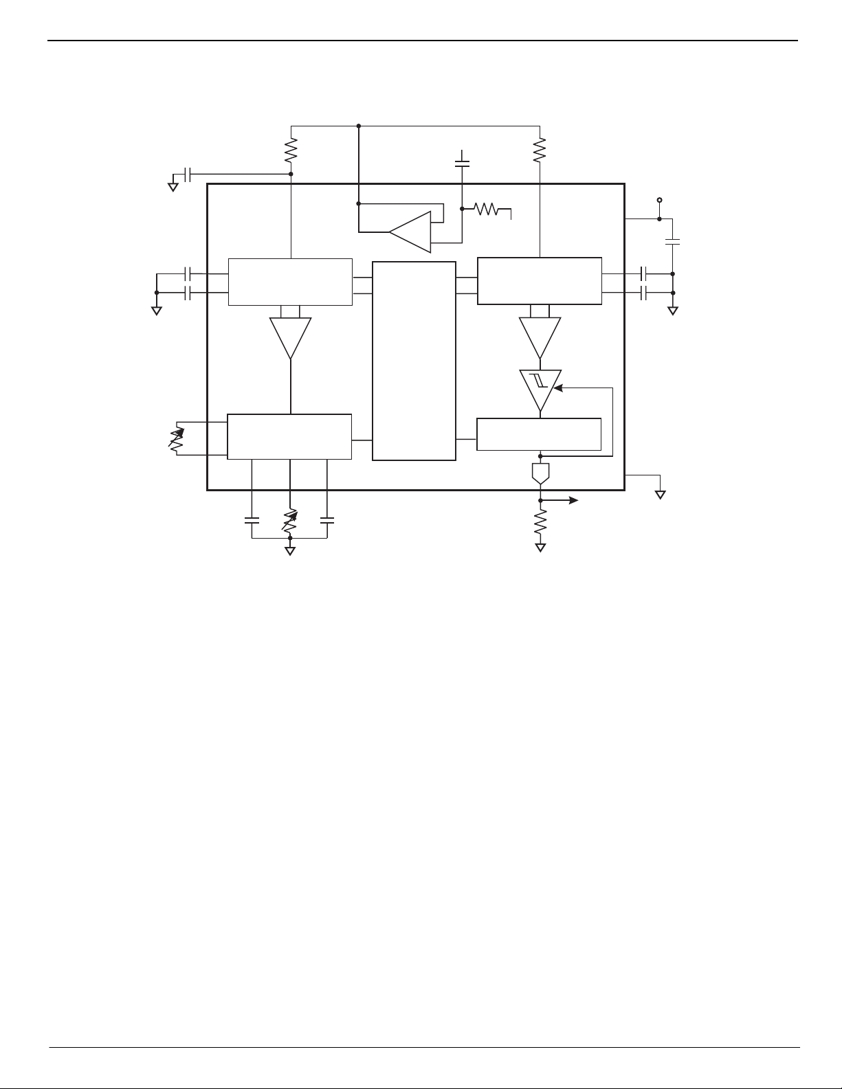
3. External Components
V
R1
DD
C6
V
Signal Input
C4
C3
C3
C2
C2
C5
1
2
R3
3
R2
4
MX105A
5
A
B
A
B
D1
6
7
8
16
15
14
13
12
11
10
R1
F
C1
A
C1
B
R4
V
SS
R
L
9
Detect Out
Figure 2: Recommended External Components
R1
See Section 5.2
F
300k
Ω
C2
See section 5.6
A
Note 2
R1
See Section 5.2
V
100k
Ω
C2
See Section 5.6
B
Note 2
R2 See Section 5.6 C3
See Section 5.8
A
Note 2
R3 See Section 5.8 C3
See Section 5.8
B
Note 2
R4 See Section 5.5 C4 See Section 5.11
Note 1, 2
R
C1
L
A
Note 4
See Section 5.2
20k
±20% C5 0.27µF ±20%
Ω
C6 0.1µF ±20%
Note 2
C1
See Section 5.2
B
Note 2
D1 See Section 5.9
Note 3
small signal
diode (1N914)
External Components Notes:
1. For improved performance, C4 may be chosen to provide 30° phase shift at the VCO loop filter input.
2. For compatibility with the MX105; capacitors (C1 - C4) may be connected to V
instead of VSS.
DD
3. For improved de-response time, a diode (D1) may be added.
4. Any value load resistance (R
) may be used, providing the maximum load current does not exceed the value
L
given in ‘Maximum Ratings Specifications’.
© 1997 MX•COM, INC. www.mxcom.com Tele: 800 638 5577 910 744 5050 Fax: 910 744 5054 Doc.# 20480133.003
4800 Bethania Station Road, Winston-Salem, NC 27105-1201 USA All trademarks and service marks are held by their respective companies.
Page 6

Tone Detector 6 MX105A PRELIMINARY INFORMATION
4. General Description
The MX105A implements a frequency detector with a phase locked loop (PLL) and a lock detector. The voltage controlled
oscillator (VCO) center frequency, detection bandwidth, loop filter, and detect filter are all independently controlled by
external components.
The MX105A provides a pair of pseudo-sinewave multipliers for splitting the input signal into approximately orthogonal
components. These multipliers are implemented with commutating filters (cyclically sampling filters) which translate an in
band AC input signal to DC. The commutating loop filter is used as the phase detector of the PLL while the commutating
detect filter provides for lock detection. Each pseudo-sinewave has a cyclic form (1 1 0 -1 -1 0) to eliminate low order
harmonic responses. The loop filter produces an error signal, which when applied to the VCO input allows frequency
locking. A limiter between the loop filter output and the VCO input provides tunable control of the detection bandwidth
(BW). Once lock is achieved the detect filter produces a DC value proportional to the input tone amplitude. An internally
generated reference is compared to the detect filter output to determine whether the PLL is locked to an input tone. Once
lock is determined the internal reference is reduced by 50% to minimize output chatter with marginal input signals.
The sampling clocks of the detect filter lag those of the loop filter by 60°. To improve performance, a capacitor (C4) can
be used to phase shift the input to the loop filter by 30°. This shifts all sampling clocks an additional 30° relative to the
input tone to phase align the detect filter sampling clocks with the amplitude peaks of the input tone.
Figure 3 shows the sampling clocks relative to an in band input tone; this figure represents the steady state ‘locked’
condition without C4.
Internal Clock
Logic 1
indicates
sampling
period
Segment
Input T one
C2
C2
C3
C3
5
4
B
A
A
B
Figure 3: Sampling Clocks of Commutating Filters
6123456123456123
© 1997 MX•COM, INC. www.mxcom.com Tele: 800 638 5577 910 744 5050 Fax: 910 744 5054 Doc.# 20480133.003
4800 Bethania Station Road, Winston-Salem, NC 27105-1201 USA All trademarks and service marks are held by their respective companies.
Page 7

Tone Detector 7 MX105A PRELIMINARY INFORMATION
5. Application
The external components shown in Figure 2 are used to adjust the various performance parameters of the MX105A. The
signal-to-noise performance, response time and signal bandwidth are all interrelated factors which should be optimized to
meet the requirements of the application.
By selecting component values in accordance with the following formulas, optimum circuit performance is obtained for any
given application.
First define the following application parameters:
A. The center frequency to be detected (f
B. The MX105A Minimum Usable Bandwidth (MUBW). This is obtained by taking into account the worst case
tolerances on the input tone frequency and variations in the MX105A f
effect of the MX105A and its supporting components.
C. The maximum permissible MX105A response time.
D. The minimum input signal amplitude.
Note: Using this information the appropriate component values can be calculated, and the signal-to-noise performance
can be read from a chart. Do not add large safety margins for response time and minimum signal amplitude;
reasonable margins are already included in the formulas. Excessive margins may result in reduced noise immunity.
5.1 Method for Calculating External Component Values
The examples on the following pages demonstrate the calculation of component values for any given application. For the
purpose of the examples, the values below are used:
A. f
= 2800 Hz
0
B. ∆TEMP = 100 °C, ∆ V
C. Maximum allowed response time = 50ms
D. Minimum input signal amplitude = 200 mV
= 1V, ∆fIN = 0.5%
DD
).
0
due to supply voltage and any temperature
0
.
RMS
5.2 Define f
The components R1, C1
0
and C1B set the free running frequency of the VCO and therefore the f0 of the MX105A. As
A
shown below, the frequency of 2800 Hz corresponds to a capacitor value of 220pF and a resistor value of 385 kΩ. This
resistance can be achieved with a 300 kΩ fixed resistor for R1
C1
and C1B should include 10-20pF parasitic capacitance due to the device and its package plus any board parasitic
A
and for R1V a 100 kΩ potentiometer. The capacitance of
F
capacitance.
=
f
0
⋅+
K R1(C1 C1 )
1
AB
⇒× =
R1 C1
A
2Kf
1
0
where : K = 2.1 ± 5%
R1 = (R1
+ R1V)
F
5.3 Calculate Minimum Usable Bandwidth
Minimum Usable Bandwidth (MUBW) is the TOTAL bandwidth required for the following:
A. Input signal frequency tolerance
B. MX105A f
C. MX105A f
Note: Add A, B and C and express as TOTAL bandwidth, not as a ± percentage (%) value.
temperature coefficient (TC = 100 ppm/°C)
0
supply voltage coefficient (VC = 5000 ppm/V)
0
MUBW f TEMP V= + T + V
∆∆ ∆
0
CC
MUBW = 0.5 + 0.01 100 + 0.5 1 = 2%
××
5.4 Calculate The Recommended Operating Bandwidth
+
10 MUBW210 2
=
BW
© 1997 MX•COM, INC. www.mxcom.com Tele: 800 638 5577 910 744 5050 Fax: 910 744 5054 Doc.# 20480133.003
4800 Bethania Station Road, Winston-Salem, NC 27105-1201 USA All trademarks and service marks are held by their respective companies.
+
=
=
6%
2
Page 8

Tone Detector 8 MX105A PRELIMINARY INFORMATION
5.5 Select R4 for Operating BW
R4
=
10.35 BW
=
−
×
4.8 BW
The exact bandwidth given by any value of R4 will vary slightly. In applications where an exact bandwidth is required, R4
should be a variable resistor to permit adjustment.
×
4.8 6
10.35 6
−
≈Ω
6.8k
5.6 Calculate R2×C2
For a frequency of 2800 Hz, a bandwidth of 6%, and a choice of
A
×≈
R2 C2
A
100
××
3f BW
0
=⇒=µΩ
C2 0.01 F R 200k
AV
.
Note: Use nearest preferred values.
5.7 Define Maximum Allowed Response Time
The maximum response time (TON) is the sum of the VCO lock time (T
The MX105A’s T
must not exceed the maximum time allowed for the application, but a value lying near the maximum
ON
gives the best S/N performance.
A. Calculate T
LOCK
T
LOCK
150
=
×
fBW
0
Using the formula above, for a frequency of 2800 Hz and a bandwidth of 6% the approximate Lock time (T
ms. Since the maximum response time is 50 ms, a DETECT time of 41 ms is allowed.
Note: T
B. Calculate Maximum Allowable T
C. Define Minimum Expected Signal Amplitude
This is used in calculating T
may vary from near zero to the value given, causing corresponding variations in actual TON.
LOCK
DETECT
DETECT
components.
TTT
DETECT ON LOCK
()
=−
V
IN
MIN
MAX
) and the DETECT integration time (T
LOCK
LOCK
DETECT
) will be 9
).
5.8 Calculate R3×C3
A
Note:
1. For a signal amplitude of 200 mV
a T
DETECT
time of 20ms. This in turn yields a response time of 9ms + 20 ms = 29ms.
2. Use nearest preferred values.
T
R3 C3
×≈
A
where: V
, a resistor value R3 of 510 kΩ with a 0.1µF capacitor for C3A and C3B will yield
RMS
is the detect filter sensitivity.
TH
DETECT
3ln1
−× −
V
V
IN
TH
MIN
© 1997 MX•COM, INC. www.mxcom.com Tele: 800 638 5577 910 744 5050 Fax: 910 744 5054 Doc.# 20480133.003
4800 Bethania Station Road, Winston-Salem, NC 27105-1201 USA All trademarks and service marks are held by their respective companies.
Page 9

Tone Detector 9 MX105A PRELIMINARY INFORMATION
5.9 Calculate Maximum De-response Time
T3ln
≈− ×
OFF
where: V
is the detect filter sensitivity.
TH
V
TH
V
IN
MAX
R3 C3
×
A
For improved de-response time, a diode (1N914 or similar) can be placed between pins 5 and 6, as shown in Figure 3.
The formula and figure below show the approximate time the MX105A will take to turn off after an in-band signal has been
removed. The effect of this diode is to greatly reduce the turn-off time with signal input amplitudes greater than 300
mV
. This graph is for VDD = 5V; for lower VDD KDT increases.
RMS
≈××
T K R3 C3
OFF
3.8
3.6
3.4
3.2
3.0
2.8
De-response with Diode
DT A
K = Number of RCTime Constants for
DT
2.6
2.4
2.2
0 80 160 240 320 400 480 560 640 720
Figure 4: K
Factor for T
DT
Input Signal Level (mV )
vs. Signal Input Amplitude
OFF
RMS
© 1997 MX•COM, INC. www.mxcom.com Tele: 800 638 5577 910 744 5050 Fax: 910 744 5054 Doc.# 20480133.003
4800 Bethania Station Road, Winston-Salem, NC 27105-1201 USA All trademarks and service marks are held by their respective companies.
Page 10

Tone Detector 10 MX105A PRELIMINARY INFORMATION
g
5.10 Calculate Signal to Noise Performance
Worst-case S/N calculations depend on calculation of a value “M” using the formula shown below:
R3 C3
×
×
00185.
A
A
=
.
M =
∞
M = 1
M
=
3R2C2
××
substituting example values,
510 0.1
=
M
××
3200
By substituting this value for M in Figure 5, the minimum required S/N of an in band tone with respect to an adjacent
interfering tone can be found. This then has to be increased depending on the input tone amplitude.
-28
-24
-20
M = 0.33
-16
M = 0.1
-12
-8
-4
0
1
24
6810
Number of Bandwidths Separation
Figure 5: S/N vs. BW Separation
The following formula expresses the reduction in noise immunity as the input signal approaches the detect filter sensitivity
.
V
TH
required
S
= 20lo
N
V
VV
IN TH
+
S
N
Figure 5
IN
−
If this S/N is better than required for the application, R3×C3
can be reduced, or the operating bandwidth can be
A
increased to obtain a faster tone detection time.
If the S/N performance is not adequate, the operating bandwidth can be reduced toward the MUBW, or R3C3
can be
A
increased to improve S/N performance at the expense of slower response time.
5.11 Calculate C4 for 30° Phase Shift
Capacitor C4 is used to phase shift the input to the VCO commutating filter by 30°, thereby shifting the sampling clocks by
the same amount. This enables the Detect sampling filter to sample and integrate at the maximum and minimum of the
input tone.
°
C4
© 1997 MX•COM, INC. www.mxcom.com Tele: 800 638 5577 910 744 5050 Fax: 910 744 5054 Doc.# 20480133.003
4800 Bethania Station Road, Winston-Salem, NC 27105-1201 USA All trademarks and service marks are held by their respective companies.
××
π
2f
R R
0V0V
tan(30 )
=
≈
0.092
×
f
≈
164pF
Page 11

Tone Detector 11 MX105A PRELIMINARY INFORMATION
6. Performance Specification
6.1 Electrical Performance
6.1.1 Absolute Maximum Ratings
Exceeding these maximum ratings can result in damage to the device.
General Min. Max. Units
Supply (VDD - VSS) -0.3 7.0 V
Voltage on any pin (wrt VSS) -0.3 V
Current
V
DD
V
SS
-30 30 mA
-30 30 mA
Any other pins -20 20 mA
Max. Output Switch Load Current 10 mA
P/LH/DW Package
Device Dissipation at T
= 25°C 800 mW
AMB
Derating above 25°C 13 mW/°C above 25°C
Storage Temperature -40 85 °C
Operating Temperature -30 85 °C
+ 0.3 V
DD
6.1.2 Operating Limits
Correct operation of the device outside these limits is not implied.
Notes Min. Typ. Max. Units
Supply (VDD - VSS) 2.7 3.3/5.0 5.5 V
Operating Temperature -30 85 °C
© 1997 MX•COM, INC. www.mxcom.com Tele: 800 638 5577 910 744 5050 Fax: 910 744 5054 Doc.# 20480133.003
4800 Bethania Station Road, Winston-Salem, NC 27105-1201 USA All trademarks and service marks are held by their respective companies.
Page 12

Tone Detector 12 MX105A PRELIMINARY INFORMATION
6.1.3 Operating Characteristics
For the following conditions unless otherwise specified:
V
= 5.0 V @ T
DD
AMB
= 25°C
Load resistance on decoder output = 20kΩ.
Notes Min. Typ. Max. Units
Static Parameters
I
DD
Amplifier Input Impedance 160 200
Digital Output Impedance 500 1000
Analog Output Impedance 1000 1200
1.0 mA
k
Ω
Ω
Ω
Dynamic Parameters
Input Signal
Frequency 40 20,000 Hz
Lowest Must Detect Level 1 30 mV
Highest Will Not Detect Level 1 20 mV
Highest Will Not Detect f0/2 1, 2 30
790
Highest Will Not Detect 5(f0) 1, 2 20
250
mV
mV
RMS
RMS
dB
RMS
dB
RMS
VCO
Frequency 3 120 120,000 Hz
Frequency Stability 100 ppm/°C
5000 ppm/V
BW Limiter
BW Range 2 10 %f
0
Amplifier
Open Loop Gain 60 dB
GBWP 1.0 MHz
Closed Loop Gain 0 dB
Detect Commutating Filter
Sensitivity (VTH)125mV
RMS
Operating Characteristics Notes:
1. Multiply by V
2. The reference level is V
/5V for other supply values.
DD
. The following formula converts dB to mV
TH
mV = V
RMS
10
(dB/20)
×
RMS
TH
.
3. Observing pins 13, 14, or 15 (DW/J package) will cause a frequency shift due to additional loading. If tuning center
frequency by observing oscillator, design in a buffer amplifier between pin 15 and probe/calibration point and tune with
no input signal. Otherwise, tune by observing detect output band edges while sweeping input signal. VCO center
frequency is 6(f
© 1997 MX•COM, INC. www.mxcom.com Tele: 800 638 5577 910 744 5050 Fax: 910 744 5054 Doc.# 20480133.003
4800 Bethania Station Road, Winston-Salem, NC 27105-1201 USA All trademarks and service marks are held by their respective companies.
) at pin 15 while it is 3(f0) at pins 13 and 14.
0
Page 13

Tone Detector 13 MX105A PRELIMINARY INFORMATION
6.2 Packaging
Package Tolerances
ALTERNATIVE
PIN
LOCATION
MARKING
Y
H
A
B
E
PIN 1
X
K
C
P
J
Figure 6: 16-pin SOIC Mechanical Outline:
W
Z
DIM.
A
B
C
E
H
L
T
Order as part no. MX105ADW
J
K
L
P
T
W
X
Y
Z
NOTE: All dimensions in inches (mm.)
TYP.
0.395 (10.03)
0.286 (7.26)
0.390 (9.90)
0.013 (0.33) 0.020 (0.51)
0.041 (1.04)
0.016 (0.41)
0.050 (1.27)
0.009 (0.23) 0.0125 (0.32)
45°
0° 10°
5°
5°
Angles are in degrees
MAX.MIN.
0.413 (10.49)
0.299 (7.59)
0.105 (2.67)0.093 (2.36)
0.419 (10.64)
0.020 (0.51)0.003 (0.08)
0.050 (1.27)
7°
Figure 7: 16-pin PDIP Mechanical Outline:
Pac kageTolerances
DIM.
A
0.740 (18.80)
0.240 (6.10)
B
0.135 (3.43)
C
0.300 (7.62)
E
0.290 (7.37) 0.325 (8.26)
E1
0.015 (0.38) 0.070 (1.77)
H
0.014 (0.35) 0.023 (0.58)
J
0.040 (1.02) 0.065 (1.65)
J1
0.056 (1.42) 0.064 (1.63)
K
0.121 (3.07)
L
P
0.008 (0.20) 0.015 (0.38)
T
Y
NOTE : All dimensions in inches (mm.)
Order as part no. MX105AP
Angles are in degrees
TYP. MAX.MIN.
0.810 (20.57)
0.262 (6.63)
0.200 (5.06)
0.390 (9.91).
0.150 (3.81)
0.100 (2.54)
7e
© 1997 MX•COM, INC. www.mxcom.com Tele: 800 638 5577 910 744 5050 Fax: 910 744 5054 Doc.# 20480133.003
4800 Bethania Station Road, Winston-Salem, NC 27105-1201 USA All trademarks and service marks are held by their respective companies.
Page 14

Tone Detector 14 MX105A PRELIMINARY INFORMATION
D
E
B
Y
A
W
W
PIN 1
P
G
C
K
J
T
H
Packa geTolerances
TYP. MAX.MIN.DIM.
0.380 (9.61)
A
0.380 (9.61)
B
0.128 (3.25)
C
0.417 (10.60)
D
0.417 (10.60)
E
F
G
H
J
0.047 (1.19)
K
0.049 (1.24)
P
0.006 (0.152)
T
30°
W
Y
NOTE: All dimensions in inches (mm.)
0.250 (6.35)
0.250 (6.35)
0.023 (0.58)
Angles are in degrees
0.409 (10.40)
0.409 (10.40)
0.146 (3.70)
0.435 (11.05)
0.435 (11.05)
0.022 (0.55)0.018 (0.45)
0.048 (1.22)
0.051 (1.30)
0.009 (0.22)
45°
6°
F
Figure 8: 24-pin PLCC Mechanical Outline:
Order as part no. MX105ALH
© 1997 MX•COM, INC. www.mxcom.com Tele: 800 638 5577 910 744 5050 Fax: 910 744 5054 Doc.# 20480133.003
4800 Bethania Station Road, Winston-Salem, NC 27105-1201 USA All trademarks and service marks are held by their respective companies.
 Loading...