

Page 1
DATA BULLETIN
MX102
© 1997 MX•COM,INC. www.mxcom.com Tele: 800 638 5577 910 744 5050 Fax: 910 744 5054 Doc.# 20480095.003
4800 Bethania Station road, Winston-Salem, NC 27105-1201 USA All trademarks and service marks are held by their respective companies.
Autocorrelating
Si
g
nal Processor
Features Applications
•
Low Signal Level Input of 10mVrms
•
Wide Signal Frequency Range from 17Hz to 13kHz
•
On-Chip Gain Amplifier
•
Digital Output Signal (f
IN
x 4)
•
Divided-Down Clock Output
•
Low Supply Voltage Operation of 2.5 V
•
Low Current Drain
•
Medical Instruments
•
Sonar Detection
•
Remote Signaling
•
Pagers
•
Mobile Radio
•
Slow Data Rate Communication
•
Tone Detection
SIGNAL IN
SIGNAL BIAS
AUTOCORRELATION
PROCESS
OUTPUT
[4 x SIGNAL IN]
Output
CLOCKS
XT AL
V
DD
V
SS
XTAL/CLOCK
GENERAT OR/
DIVIDER
-
+
DELAY
48-BIT
COMPARE
LOGIC
DELAY
48-BIT
INTERPOLATE
INTERPOLATE
OUTPUT
LOGIC
DELAY
24-BIT
COMPARE
LOGIC
DELAY
24-BIT
XT AL/CLOCK
CLOCK
6
BUFCLK
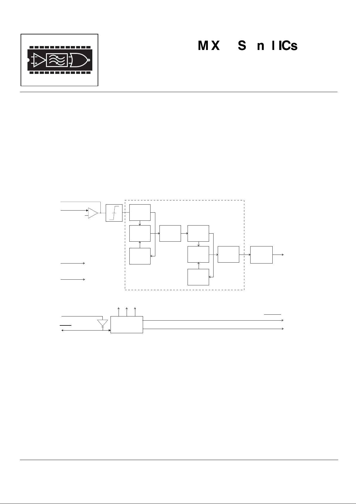
The MX102 is a single-chip device to extract single periodic signals from very high random-noise environments.
Using patented autocorrelation techniques the MX102 will enhance the input signal's signal-to-noise ratio by as much as
8.5dB and provide a digital output signal centered at four times (x4) the input frequency.
The amplitude of non-periodic components of the signal is substantially reduced. The patented autocorrelator compares
the incoming signal to itself; the more elements of the waveform that are seen as periodic, the higher the energy at the
microcircuit output.
The MX102 cascades two autocorrelators, each one improving the signal-to-noise ratio
With a random noise input the output will swing rail-to-rail at random (peak-limited). The input/output signal delay is fixed
by the choice of clock frequency and the length of the internal register. The MX102 will operate at supply voltages of
between 2.5 volts and 5.5 volts and with Xtal/clock frequencies from 20kHz to 2.5MHz. Using various Xtal/clock inputs the
device can be set to accept input signal frequencies, in bands, from 17.0Hz to 13.0kHz.
Two uncommitted clock outputs are available: one to supply a 'divided-down' Xtal/clock frequencies and the second is a
buffered output for use in external and peripheral functions.
This MX102 is available in the following package styles: 16-pin SOIC (MX102DW) and 16-pin CDIP (MX102J).
Page 2

Autocorrelating Signal Processor 2 MX102
© 1997 MX•COM,INC. www.mxcom.com Tele: 800 638 5577 910 744 5050 Fax: 910 744 5054 Doc.# 20480095.003
4800 Bethania Station road, Winston-Salem, NC 27105-1201 USA All trademarks and service marks are held by their respective companies.
CONTENTS
Section Page
1. Block Diagram.................................................................................................................................. 3
2. Signal List......................................................................................................................................... 4
3. External Components...................................................................................................................... 5
4. General Description......................................................................................................................... 6
4.1 Signal........................................................................................................................................................ 6
4.2 Input Frequency Range.............................................................................................................................6
5. Performance Specification.............................................................................................................. 8
5.1 Electrical Performance..............................................................................................................................8
5.2 Packaging ................................................................................................................................................ 10
MX•COM, Inc. reserves the right to change specifications at any time and without notice.
Page 3
Autocorrelating Signal Processor 3 MX102
© 1997 MX•COM,INC. www.mxcom.com Tele: 800 638 5577 910 744 5050 Fax: 910 744 5054 Doc.# 20480095.003
4800 Bethania Station road, Winston-Salem, NC 27105-1201 USA All trademarks and service marks are held by their respective companies.
1. Block Diagram
SIGNAL IN
SIGNAL BIAS
AUTOCORRELATION
PROCESS
OUTPUT
[4 x SIGNAL IN]
Output
CLOCKS
XTAL
V
DD
V
SS
XTAL/CLOCK
GENERATOR/
DIVIDER
-
+
DELAY
48-BIT
COMPARE
LOGIC
DELAY
48-BIT
INTERPOLATE
INTERPOLATE
OUTPUT
LOGIC
DELAY
24-BIT
COMPARE
LOGIC
DELAY
24-BIT
XTAL/CLOCK
CLOCK
6
BUFCLK
Figure 1: Device Block Diagram
Page 4

Autocorrelating Signal Processor 4 MX102
© 1997 MX•COM,INC. www.mxcom.com Tele: 800 638 5577 910 744 5050 Fax: 910 744 5054 Doc.# 20480095.003
4800 Bethania Station road, Winston-Salem, NC 27105-1201 USA All trademarks and service marks are held by their respective companies.
2. Signal List
Packages Signal Description
DW/J Name Type
1 Signal In input The inverting input to the analog amplifier/comparator. Used with the
Signal Bias pin; external coupling components are required.
See Figure 2
3 Signal
Bias
output The output of the analogue amplifier/comparator. Do not load this pin with
peripheral circuitry; there is no drive capacity for off-chip signaling. The
feedback resistor should be not less than 200kΩ. See Figure 2.
4V
DD
power Positive supply rail. A single, stable power supply is required. Note that
this device has two V
DD
pins; this input is positioned to prevent cross-talk,
either or both may be connected to the host circuit's supply line. Do not
attempt to draw current from either V
DD
pin.
5 BUFCLK output Buffered inverter oscillator digital output. May be used as test point to
align clock frequency or to drive other circuitry.
6
XTAL
output The output of the on-chip clock oscillator inverter.
8 Xtal/Clock input
The input to the on-chip clock oscillator inverter; this may be a Xtal,
resonator or clock pulse input. The selection of this frequency will affect
the operational input signal bandwidth (and output frequency) of this
device; refer to Table 4. Note that the choice of V
DD
will determine the
maximum Xtal/clock frequency and hence the maximum useable signal
input frequency. Operation of this microcircuit without an active Xtal or
clock input may cause device damage. A clock pulse input is fed directly
into this pin; Xtal/clock components are not required.
See Table 2.
9V
SS
power Negative Supply
11 CLK ÷ 6 output A squarewave output clock signal at the rate of Clock/6; provided for
peripheral and test purposes.
13 OUTPUT output
(fOUT = 4 x fSIGNAL IN). The auto-correlated output signal at four times
(x 4) the input signal (see Figure 3).
There is a time delay between input and output signals (see
Specifications).
16 V
DD
power
Positive supply rail. A single, stable power supply is required.
Note that this device has two VDD pins; either or both may be connected
to the host circuit's supply line. Do not attempt to draw current from either
V
DD
pin.
The choice of V
DD
will determine the maximum Xtal/clock frequency and
hence the maximum useable signal input frequency (see Figure 4).
2, 7, 10, 12, 14, 15 N/C No internal connection. Leave open circuit
Table 1: Signal List
Page 5

Autocorrelating Signal Processor 5 MX102
© 1997 MX•COM,INC. www.mxcom.com Tele: 800 638 5577 910 744 5050 Fax: 910 744 5054 Doc.# 20480095.003
4800 Bethania Station road, Winston-Salem, NC 27105-1201 USA All trademarks and service marks are held by their respective companies.
VDD (V) Max. Xtal/Clock Freq. (MHz)
2.5 0.625
3.0 1.0
5.0 2.5
Table 2: Maximum Usable Xtal/Clock Frequencies
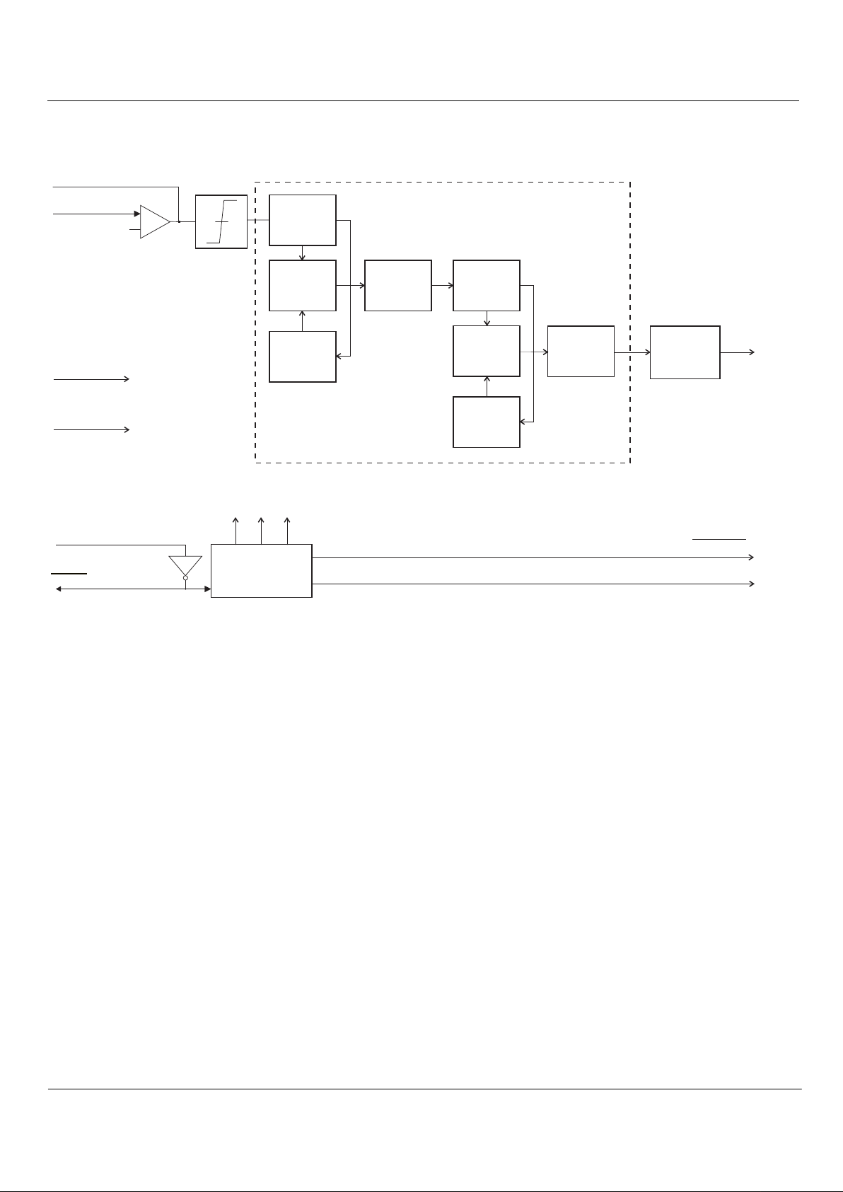
3. External Components
V
DD
V
V
DD
V
DD
C5
R1
C1
V
SS
1
2
3
4
5
6
7
8
16
15
14
13
12
11
10
9
SIGNAL IN
BUFCLK
SIGNAL
INPUT
OUTPUT
(f = 4 x SIGNAL IN)
x
x
x
x
x
x
SIGNAL BIAS
CLOCK
OUTPUT
6
MX102
XTAL
XTAL/CLOCK
6
8
C3
C2
C4
X
1
R2
XTAL
XTAL/CLOCK
Figure 2: Recommended External Components
R1
2.2M
Ω
R2
1.0M
Ω
C1 0.01µF
C2 Note 1 47.0pF -see below
C3 Note 1 47.0pF -see below
C4 Note 2 5 - 65pF -see below
C5 1.0µF
X1 560kHz resonator
X1 range 20kHz to 2.5MHz
Table 3: Recommended External Components
Recommended External Component Notes:
1. Values of capacitors C2 and C3 should be reduced for higher Xtal frequencies and/or lower supply voltages (V
DD
).
2. C4 is suggested for frequency setting when using a resonator; when a Xtal is used C4 is omitted.
Page 6

Autocorrelating Signal Processor 6 MX102
© 1997 MX•COM,INC. www.mxcom.com Tele: 800 638 5577 910 744 5050 Fax: 910 744 5054 Doc.# 20480095.003
4800 Bethania Station road, Winston-Salem, NC 27105-1201 USA All trademarks and service marks are held by their respective companies.
4. General Description
4.1 Signal
f
SIGNAL IN
f
OUT
=4xf
SIGNAL IN
SIGNAL OUT
Frequency
Level
SIGNAL IN
Figure 3: MX102 Input/Output Relationships
Note:
1. The frequency of the output signal is four times (x4) that of the input signal.
4.2 Input Frequency Range
The MX102 has a wide frequency range, but care must be taken to choose the Xtal frequency appropriate for your
application.
Xtal/Clock Frequency
(kHz)
Input Freq. (Hz) BW (Hz)
Min. Max.
20 17 105 88
100 88 526 443
200 166 1052 886
300 250 1579 1329
400 333 2105 1772
500 416 2632 2216
560 467 2947 2480
600 500 3158 2658
700 583 3684 3101
800 667 4210 3543
900 750 4737 3987
1000 833 5263 4430
2000 1667 10526 8859
2500 2083 13157 11074
Table 4: Input Signal Ranges vs Xtal/Clock Frequency
Page 7

Autocorrelating Signal Processor 7 MX102
© 1997 MX•COM,INC. www.mxcom.com Tele: 800 638 5577 910 744 5050 Fax: 910 744 5054 Doc.# 20480095.003
4800 Bethania Station road, Winston-Salem, NC 27105-1201 USA All trademarks and service marks are held by their respective companies.
0
2000
4000
6000
8000
10000
12000
14000
Maximum Input Frequency (Hz)
Minimum Input Frequency (Hz)
Input Signal Bandwidth (Hz)
Maximum Clock Limit
at V
DD
=2.5V
Maximum Clock Limit
at V
DD
=3.0V
For V
DD
=5.0V
Input Signal Frequency (Hz)
Xtal/Clock Frequency (kHz)
0 500 1000 1500 2000 2500
Minimum Input Frequency =
Xtal/Clock Frequency (Hz)
1200
Maximum Input Frequency =
Xtal/Clock Frequency (Hz)
190
Figure 4: Input Signal Ranges vs Xtal/Clock Frequency
Effective Output Signal-to-Noise Ratio (dB)
Input Signal = 2.7kHz 20mVrms
Xtal/Clock Frequency 500kHz
V
DD
=5.0V
Input Signal-to-Noise Ratio (dB)
1
2
3
4
5
6
7
8
9
-6 -5 -4 -3 -2 -1 0 1 2 3 4 5 6 7 8
Figure 5: Enhancement of Signal-To-Noise Ratio
Note:
1. The graph shown in Figure 5 illustrates the signal-to-noise enhancement that can be obtained, under varying input
conditions, from the MX102.
Page 8
Autocorrelating Signal Processor 8 MX102
© 1997 MX•COM,INC. www.mxcom.com Tele: 800 638 5577 910 744 5050 Fax: 910 744 5054 Doc.# 20480095.003
4800 Bethania Station road, Winston-Salem, NC 27105-1201 USA All trademarks and service marks are held by their respective companies.
5. Performance Specification
5.1 Electrical Performance
Absolute Maximum Ratings
Exceeding these maximum ratings can result in damage to the device.
General Min. Max. Units
Supply Voltage -0.3 7.0 volts V
Input Voltage at any pin -0.3 (VDD+0.3 volts) V
Current
V
DD
-30 30 mA
V
SS
-30 30 mA
Any other pins -20 20 mA
Maximum Device Dissipation 100 mW
Operating Temperature -40° 85 °C
Storage Temperature -40° 125 °C
Operating Limits
Correct operation of the device outside these limits is not implied.
Min. Typ. Max. Units
V
DD
2.5 3.3/5.0 5.5 V
Xtal/Clock 20 2500 kHz
Operating Temperature -40 85 °C
Page 9

Autocorrelating Signal Processor 9 MX102
© 1997 MX•COM,INC. www.mxcom.com Tele: 800 638 5577 910 744 5050 Fax: 910 744 5054 Doc.# 20480095.003
4800 Bethania Station road, Winston-Salem, NC 27105-1201 USA All trademarks and service marks are held by their respective companies.
Operating Characteristics
For the following conditions unless otherwise specified:
V
DD
= 5.0V, T
AMB
= 25°C
Xtal/Clock = 560kHz, Input Test Signal = 200mV
RMS
Notes Min. Typ. Max Units
Static Values
Supply Current - 1.0 2.5 mA
2 - 4.0 - mA
Logic ‘1’ Level 80% - - V
Logic ‘0’ Level - - 20% V
Digital Output Impedance - 4.0 10.0
k
Ω
Dynamic Values
Signal Input 3 20.0 - 1000 mV
RMS
Analog (Input) Amplifier Gain 4 20.0 - - dB
5 9.0 - - dB
6 10.0 - - dB
Recommended Input Signal Duty Cycle Ratio 35 50 - %
Frequency Out/Frequency In Ratio 4.0 - 4.0 %
Maximum Xtal/Clock Frequency 1 2.5 - - MHz
Minimum Xtal/Clock Frequency 20.0 kHz
Frequency Input Range
Xtal/Clock = 560kHz 7 500 - 3000 Hz
Table 4 1/1200 1/190 Xtal/Clock
Input to Output Delay 8 - 1.4 ms
Output resolution - 1/6 - Xtal/Clock
Operating Characteristics Notes:
1. Maximum Xtal/clock frquency allowed varies with applied supply voltage (V
DD
).
2. I
DD
requirement for Xtal/clock frequency of 2.24MHz.
3. Signal input level required to provide a constant autocorrelated output.
4. Measured with a 6.0kHz sinewave at the signal input.
5. Measured with V
DD
= 2.5 volts.
6. Measured with a 12kHz input signal.
7. Recommended input signal frequency range to correlation circuits.
8. Input (Signal In) to output (Output) time with a 2.24MHz Xtal/clock input.
Page 10
Autocorrelating Signal Processor 10 MX102
© 1997 MX•COM,INC. www.mxcom.com Tele: 800 638 5577 910 744 5050 Fax: 910 744 5054 Doc.# 20480095.003
4800 Bethania Station road, Winston-Salem, NC 27105-1201 USA All trademarks and service marks are held by their respective companies.
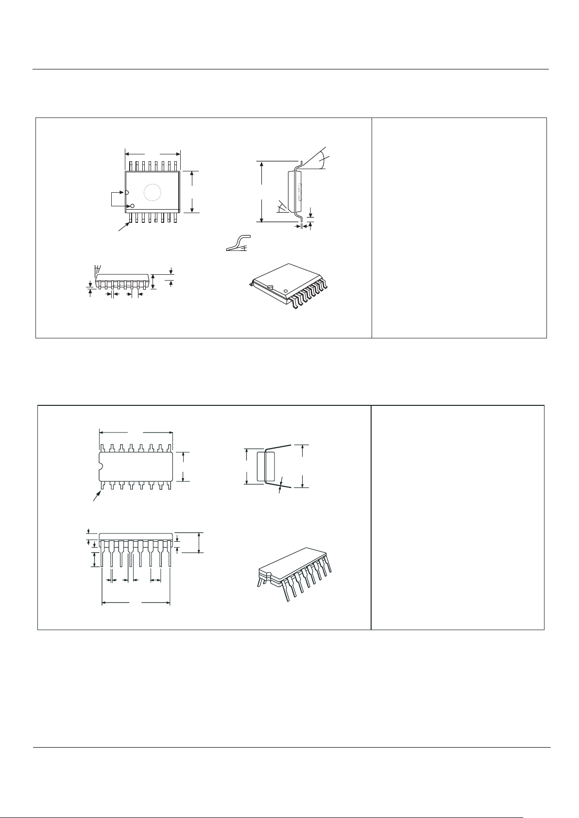
5.2 Packaging
PIN 1
A
B
ALTERNATIVE
PIN
LOCATION
MARKING
X
P
J
Y
C
K
H
E
L
T
W
Z
NOTE: All dimensions in inches (mm.)
Angles are in degrees
Packa geTolerances
A
B
C
E
H
TYP.
MAX.MIN.
DIM.
J
P
X
W
T
Y
K
L
0.105 (2.67)0.093 (2.36)
0.419 (10.64)
45°
7°
0° 10°
0.050 (1.27)
0.041 (1.04)
0.413 (10.49)
0.299 (7.59)
0.050 (1.27)
0.016 (0.41)
0.390 (9.90)
0.020 (0.51)0.003 (0.08)
0.009 (0.23) 0.0125 (0.32)
0.013 (0.33) 0.020 (0.51)
0.395 (10.03)
0.286 (7.26)
Z
5°
5°
Figure 6: 16-pin SOIC Mechanical Outline:
Order as part no. MX102DW
B
A
PIN 1
E1
T
E
K
H
F
J1
J
P
L
C
K1
PackageTolerances
NOTE : All dimensions in inches (mm.)
Angles are in degrees
TYP.
MAX.MIN.
A
B
C
E
E1
F
H
DIM.
J
J1
P
T
K1
K
L
0.230 (5.84)
0.291 (7.39)
0.415 (10.53)
0.200 (5.08)
0.767 (19.48)
0.165 (4.19)
0.100 (2.54)
0.115 (2.92)
0.370 (9.40)
0.300 (7.61) 0.317 (8.04)
0.70 (17.78)
0.018 (0.46)
0.053 (1.33)
0.075 (1.91)
0.080 (2.03)
0.080 (2.03)
0.753 (19.13)
0.285 (7.24)
0.0102 (0.259)
0.020 (0.51)
0.055 (1.39)
0.0098 (0.249)
Figure 7: 16-pin CDIP Mechanical Outline:
Order as part no. MX102J
 Loading...