

Page 1
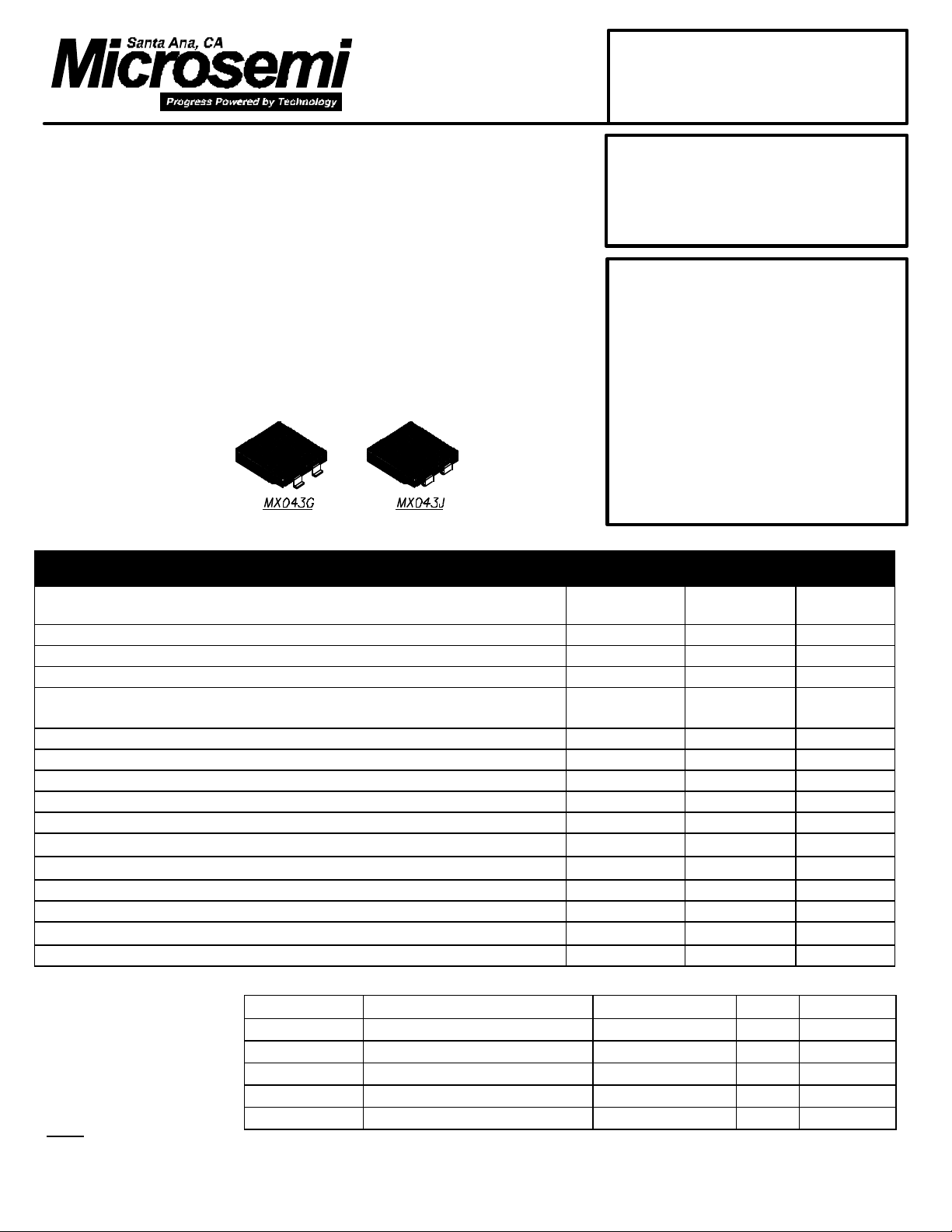
MX043G
2830 S. Fairview St.
POWER MOSFET
Santa Ana, CA 92704
PH: (714) 979-8220
FAX: (714) 966-5256
Features
• Harris FSC260R die
• total dose: 100 kRAD(Si) within pre-radiation parameter limits
• dose rate: 3 x 10⁹ RAD(Si)/sec @ 80%BV
• dose rate: 2 x 10
• neutron: 1013 neutrons/cm2 within pre-radiation parameter limits
• photocurrent: 17 nA/RAD(Si)/sec typical
• rated Safe Operating Area Curve for Single event Effects
• rugged polysilicon gate cell structure with ultrafast body diode
• low inductance surface mount power package available with “J-leads”
(MX043J) or “gullwing-leads” (MX043G)
• very low thermal resistance
• reverse polarity available upon request add suffix “R”st
12
RAD(Si)/sec @ ID ≤ IDM typical
DSS
typical
MX043J
200 Volts
44 Amps
50 mΩ
RADIATION
HARDENED
SEGR-RESISTANT
N-CHANNEL
ENHANCEMENT
MODE
Maximum Ratings @ 25°C (unless otherwise
DESCRIPTION SYMBOL MAX. UNIT
Drain-to-Source Breakdown Voltage (Gate Shorted to Source)
@ TJ ≥ 25°C
Drain-to-Gate Breakdown Voltage @ T
≥ 25°C, RGS= 1 MΩ BV
J
Continuous Gate-to-Source Voltage V
Transient Gate-to-Source Voltage V
Continuous Drain Current Tj= 25°C
Tj= 100°C
Peak Drain Current, pulse width limited by T
Jmax
Repetitive Avalanche Current I
Repetitive Avalanche Energy E
Single Pulse Avalanche Energy E
Power Dissipation P
Junction Temperature Range T
Storage Temperature Range T
Continuous Source Current (Body Diode) I
Pulse Source Current (Body Diode) I
Thermal Resistance, Junction to Case
Weight - grams
BV
I
DSS
DGR
GS
GSM
I
D25
D100
I
DM
AR
AR
AS
D
j
stg
S
SM
θ
JC
200 Volts
200 Volts
+/-20 Volts
+/-30 Volts
44
28
132 Amps
44 Amps
tbd mJ
tbd mJ
300 Watts
-55 to +125
-55 to +125
44 Amps
132 Amps
0.25
Amps
°C
°C
°C/W
SINGLE EVENT Ion Species typical LET (MeV/mg/cm)
EFFECTS Ni 26 43 -20V 200V
SAFE Br 37 36 -5V 200V
OPERATING Br 37 36 -10V 160V
AREA Br 37 36 -15V 100V
(SEESOA) Br 37 36 -20V 40V
Notes
(1) Pulse test, t ≤ 300 µs, duty cycle δ ≤ 2%
(2) Microsemi Corp. does not manufacture the mosfet die; contact company for details.
Datasheet# MSC0857
typical range (µ)
VGS VDSmax
Page 2
MX043J
MX043G
Electrical Parameters @ 25°C (unless otherwise specified)
DESCRIPTION SYMBOL CONDITIONS MIN TYP. MAX UNIT
Drain-to-Source Breakdown Voltage
(Gate Shorted to Source)
Temperature Coefficient of the Drain-to-Source
Breakdown Voltage
Gate Threshold Voltage V
Gate-to-Source Leakage Current
Drain-to-Source Leakage Current (Zero Gate
Voltage Drain Current) I
Static Drain-to-Source On-State Resistance (1) R
Forward Transconductance (1) g
∆BV
BV
DSS
DSS
GS(th)
I
GSS
DSS
DS(on)
fs
/∆T
VGS = 0 V, ID = 1 mA 200 V
J
VDS = VGS, ID = 1 mA, TJ = 25°C
TJ = 125°C
TJ = -55°C
VGS = ± 20 VDC, VDS = 0 TJ = 25°C
TJ = 125°C
VDS =0.8•BV
= 0 V TJ = 125°C
VGS
DSS TJ
VGS= 12V, ID= 28A TJ = 25°C
ID= 25A TJ = 125°C
1.5
0.5
-
= 25°C
tbd V/°C
±100
±200
0.043-0.050
0.093
VDS ≥ 10 V; ID = 50 A 26 32 S
4.0
-
5.0
25
250
V
V
V
nA
µA
µA
Ω
Ω
Input Capacitance
Output Capacitance
Reverse Transfer Capacitance
Turn-on Delay Time
Rise Time
Turn-off Delay Time
Fall Time
Total Gate Charge
Gate-to-Source Charge
Gate-to-Drain (Miller) Charge
Body Diode Forward Voltage (1) V
Reverse Recovery Time (Body Diode) t
Mechanical Outline
ShelFit™
Q
C
T
t
C
C
d(off)
Q
Q
iss
oss
rss
d(on)
t
r
t
f
g(on)
gs
gd
SD
rr
V
= 0 V, VDS = 25 V, f = 1 MHz 4400
GS
pF
900
280
VGS = 12 V, VDS = 100 V,
ID = 44 A, RG = 2.35 Ω
40
95
ns
100
25
VGS = 12 V, VDS = 100V, ID = 44 A 160
30
83
180
38
93
nC
IF = IS, VGS = 0 V 0.6 - 1.8 V
IF = 10 A, -di/dt = 100 A/µs, TJ =25 °C 560 ns
Page 3

100% KND (Known-Good-Die) SCREENING
a. 100% die probe at T
= 25°C for BVDSS, VGSth, IDSS, IGSS, VSD, RDS
ambient
on
b. 100% Visual Inspection i.a.w. method 2072 of MIL-STD-750
DIE ELEMENT EVALUATION
a. Wafer Lot Evaluation Testing (WLAT) i.a.w. method 5001 of MIL-STD-750, including SEM
b. Unclamped Inductive Switching (I
c. Gate Stress Test for 250 µs at VGS= 30 Vdc.
d. Safe Operating Area i.a.w. method 3474 of MIL-STD-750 at VDS= 160 V, ID= 2.8 A for 10 ms
e. High Temperature Gate Bias i.a.w. method 1042 cond.B of MIL-STD-750: 48 hrs at T
VGS= 16 V
f. High Temperature Reverse Bias i.a.w. method 1042 cond.A of MIL-STD-750: 240 hrs at T
and VDS= 160 V
g. Final DC Electrical Testing at T
h. Temperature Cycling i.a.w. method 1051 of MIL-STD-750, 100 cycles, -55°C to +150°C
i. Group A Electrical Testing including dynamic parameters
j. Steady State Operational Life Bias i.a.w. method 1042 cond.A of MIL-STD-750: 1000 hrs at T
and VDS= 160 V
k. Final DC Electrical Testing at T
l. Die Attach Evaluation i.a.w. method 2017 of MIL-STD-750
m. Bond Strength Evaluation i.a.w. 2037 of MIL-STD-750
Total Dose Irradiation i.a.w. method 1019 of MIL-STD-750, dose= 100 kRAD, Drain shorted to Source, VGS= 10V
Total Dose Irradiation i.a.w. method 1019 of MIL-STD-750, dose= 100 kRAD, Gate shorted to Source, VDS= 160V
Evaluation criteria: no degradation of the DC electrical parameters exceeding the data sheet limits allowed after total dose irradiation.
) i.a.w. method 3470 of MIL-STD-750 at VGS
AS
= 25°C, 125°C and -55°C
ambient
= 25°C, 125°C and -55°C
ambient
RADIATION EVALUATION
= 15 V, L= 100µH, IAS= 132 A
peak
= 150°C, Drain shorted to Source and
ambient
= 150°C, Gate shorted to Source
ambient
= 150°C, Gate shorted to Source
ambient
Page 4

100% SCREENING
a. Internal Visual (Precap) Inspection i.a.w. method 2069 and 2072 of MIL-STD-750
b. Temperature Cycling i.a.w. method 1051 of MIL-STD-750, 10 cycles, -55°C to +125°C
c. Thermal Response i.a.w. method 3161 of MIL-STD-750
d. High Temperature Gate Bias i.a.w. method 1042 cond.B of MIL-STD-750: 24 hrs at T
VGS= 16 V
e. High Temperature Reverse Bias i.a.w. method 1042 cond.A of MIL-STD-750: 24 hrs at T
VDS= 160 V
= 125°C, Drain shorted to Source and
ambient
= 125°C, Gate shorted to Source and
ambient
f. Final electrical Testing i.a.w. this data sheet (100% DC parameters @ 25°C and sample (22/0) testing for dynamic parameters and
DC parameters @ temperature extremes)
QUALIFICATION INSPECTION
a. Thermal Resistance i.a.w. method 3161 of MIL-STD-750 - sample size= 10 devices/0 rejects
b. Solderability i.a.w. method 2026 of MIL-STD-750 - sample size= 10 devices/0 rejects
c. Temperature Cycling i.a.w. method 1051 of MIL-STD-750, 200 cycles, -55°C to +125°C - sample size 10 devices/0 rejects
d. Intermittent Operation Life i.a.w. method 1042D of MIL-STD-750 with ∆Tj= 75°C for 2000 cycles (monitoring thermal response
shift) - sample= 25 devices/0 rejects
e. Steady State Operation Life i.a.w. method 1042A of MIL-STD-750 at Tj= 115°C min. for 1000 hrs - sample= 25 devices/0 rejects
f. Steady state Gate Life i.a.w. method 1042B of MIL-STD-750 at Tj= 115°C min. for 1000 hrs. - sample= 25 devices/0 rejects
g. Safe Operating Area i.a.w. method 3474 of MIL-STD-750 (monitoring thermal response shift) - sample size= 10 devices/0 rejects
h. Shock i.a.w. method 2016 of MIL-STD-750 - sample size= 10 devices/0 rejects
i. Vibration i.a.w. method 2056 of MIL-STD-750 - sample size= 10 devices/0 rejects
j. Acceleration i.a.w. method 2006 of MIL-STD-750 - sample size= 10 devices/0 rejects
k. X-ray, one view of the die attach area (Oz axis) - sample= 10 devices/0 rejects
l. Humidity ????? - sample size= 5 devices/0 rejects
 Loading...