

Page 1
DATA BULLETIN
MX029
Dual Digitally Controlled Amplifier
1998 MX-COM, INC. www.mxcom.com Tele: 800 638 5577 910 744 5050 Fax: 910 744 5054 Doc. # 20480096.008
4800 Bethania Station Road, Winston-Salem, NC 27105-1201 USA. All trademarks and service marks are held by their respective companies.
PRELIMINARY INFORMATION
Features Applications
2 Digitally Controlled Amplifiers
±48dB Gain/Attenuation in 2dB Steps + Mute
Individual Control with a 14-Bit Serial Word
Separate Fixed Gain Buffer Amplifier
Cellular and LMR Radios
PABX’s, Electronic Mail, TAM's
Automatic Test Equipment
Remote Gain Adjustments
Digitally Set Audio Control Levels
LOAD/LATCH
DAT A INPUT
SERIAL CLOCK
SERIAL
INTERFACE
∆
G
∆
G
CH1, OUTPUT 1
STAGE 1 CONTROL REGISTER
STAGE 1 CONTROL REGISTER
TO STAGE 1
CONTROL
REGISTER
CH1, OUTPUT 2
CH2, OUTPUT 1
CH2, INPUT 2
CH2, INPUT 1
CH1, INPUT 3
CH1, INPUT 2
CH1, INPUT 1
BIAS
BIAS
BIAS
BIAS
BIAS
V
SS
V
SS
V
SS
V
SS
V
DD
UNIVERSAL
AMP OUT
UNIVERSAL
AMP IN
The MX029 Digitally Controlled Amplifier Array replaces audio level controls in radio and wireline
communications applications. It is a single-chip LSI circuit comprised of two discrete, digitally controlled gain
sections. Each section has 48 distinct gain steps (+/-48dB of range in 2dB steps) plus MUTE.
As shown in Figure 1, both gain stages have switchable inputs. This switching allows for selection of three
different input signals on one channel and two on the other channel. One of the channels also has output
switching. In addition to two digitally controlled gain stages, there is a general purpose inverting amplifier.
The gain of this amplifier is controlled externally via negative feedback. Control of each gain control section is
accomplished through the serial interface. All switching is accomplished using controlled rise and fall times,
thereby assuring no transients (clicks or pops).
The MX029 requires a single 5-volt supply and is available in the following packages: 16-pin SOIC
(MX029DW), 16-pin CDIP (MX029J), and 24-pin TSSOP (MX029TN).
Page 2

Dual Digitally Controlled Amplifier 2 MX029
1998 MX-COM, INC. www.mxcom.com Tele: 800 638 5577 910 744 5050 Fax: 910 744 5054 Doc. # 20480096.008
4800 Bethania Station Road, Winston-Salem, NC 27105-1201 USA. All trademarks and service marks are held by their respective companies.
CONTENTS
Section Page
1. Block Diagram.................................................................................................................3
2. Signal List........................................................................................................................4
3. External Components.....................................................................................................5
4. Application.......................................................................................................................5
4.1 Recommendations ................................................................................................................. 5
5. Control Data and Timing.................................................................................................6
6. Performance Specification.............................................................................................8
6.1 Electrical Performance........................................................................................................... 8
6.1.1 Absolute Maximum Ratings..........................................................................................................8
6.1.2 Operating Limits............................................................................................................................8
6.1.3 Operating Characteristics .............................................................................................................9
6.2 Serial Interface Timing ......................................................................................................... 10
6.3 Packaging............................................................................................................................. 11
MX-COM, Inc. reserves the right to change specifications at any time and without notice.
Page 3
Dual Digitally Controlled Amplifier 3 MX029
1998 MX-COM, INC. www.mxcom.com Tele: 800 638 5577 910 744 5050 Fax: 910 744 5054 Doc. # 20480096.008
4800 Bethania Station Road, Winston-Salem, NC 27105-1201 USA. All trademarks and service marks are held by their respective companies.
1. Block Diagram
LOAD/LATCH
DATA IN PUT
SERIAL CLOCK
SERIAL
INTERFACE
∆
G
∆
G
CH1, OUTPUT 1
STAGE 1 CONTROL REGISTER
STAGE 1 CONTROL REGISTER
TO STAGE 1
CONTROL
REGISTER
CH1, OUTPUT 2
CH2, OUTPUT 1
CH2, INPUT 2
CH2, INPUT 1
CH1, INPUT 3
CH1, INPUT 2
CH1, INPUT 1
BIAS
BIAS
BIAS
BIAS
BIAS
V
SS
V
SS
V
SS
V
SS
V
DD
UNIVERSAL
AMP OUT
UNIVERSAL
AMP IN
Figure 1: Device Block Diagram
Page 4
Dual Digitally Controlled Amplifier 4 MX029
1998 MX-COM, INC. www.mxcom.com Tele: 800 638 5577 910 744 5050 Fax: 910 744 5054 Doc. # 20480096.008
4800 Bethania Station Road, Winston-Salem, NC 27105-1201 USA. All trademarks and service marks are held by their respective companies.
2. Signal List
Pin No. Type Description
J, DW TN
1 1 Serial Clock This external clock input is used to “clock in” the Control Data.
See Figure 4 for timing information. This input has an internal
1M pullup resistor.
2 4 Control (Data) Input: Operation of the two amplifier channels (Ch1 - Ch2) is
controlled by the data entered serially at this pin. The data is
entered (bit 13 to bit 0) on the rising edge of the external Serial
Clock. The data format is described in Tables 1-5 and Figure 3.
This input has an internal 1M pullup resistor.
35
Load/
Latch
This function governs the loading and execution of the control
data. During serial data loading this input should be kept at a
logical “1” to ensure that data rippling past the latches has no
effect. When all 14 bits have been loaded this input should be
strobed “1 - 0 -1” to latch the new data in. Data is executed on
the rising edge of the strobe.
4 6 Ch 1 Input 1 Analog Input.
5 7 Ch 1 Input 2 Analog Input.
6 8 Ch 2 Input 1 Analog Input.
7 9 Ch 2 Input 2 Analog Input.
812 VSSNegative supply (GND).
913 V
BIAS
The output of the on-chip bias circuitry, held at VDD/2.
10 16 Ch 1 Input 3 Analog Input. Normally used for FSK data.
11 17 Ch 2 Output Analog Output.
12 18 Ch 1 Output Analog Output.
13 20 Ch 1 Output Analog Output.
14 21 Universal
Amp Out
Output from general purpose amplifier.
15 23 Universal
Amp In
Inverting input to general purpose amplifier.
16 24 V
DD
Positive supply rail. A single +5-volt power supply is required.
2, 3, 10,
11,14,
15, 19,
22
N/C No internal connection
Page 5

Dual Digitally Controlled Amplifier 5 MX029
1998 MX-COM, INC. www.mxcom.com Tele: 800 638 5577 910 744 5050 Fax: 910 744 5054 Doc. # 20480096.008
4800 Bethania Station Road, Winston-Salem, NC 27105-1201 USA. All trademarks and service marks are held by their respective companies.
3. External Components
C6
V
DD
1
2
3
4
5
6
7
89
10
11
12
13
14
15
16
Serial Clock Input
Load/Latch
Ch 1 Input 1
Ch 1 Input 2
Ch 2 Input 1
Ch 2 Input 2
C5
V
BIAS
V
SS
C1
C2
C3
C4
Serial Control Data Input Universal Amp In
Ch 1 Output 2
Ch 2 Output
Ch 1 Input 3
MX029
Ch 1 Output 1
Universal Amp Out
V
DD
C1 to C5 Note 1 0.1µF ±20%
C6 1.0µF ±20%
Notes:
1. Analog input capacitors C1 to C5 are only required for a.c. input signals; d.c. input signals do not
require these components.
Figure 2: Recommended External Components
4. Application
4.1 Recommendations
To avoid noise and instability the following practices are recommended:
1. Use a clean, well-regulated power supply.
2. Keep leads short.
3. Inputs and outputs should be shielded wherever possible.
4. Analog tracks should not run parallel to digital tracks.
5. A “Ground Plane” connected to Vss will assist in eliminating external pick-up on the channel input and
output pins.
6. Avoid running High Level Outputs adjacent to Low Level Inputs.
Page 6

Dual Digitally Controlled Amplifier 6 MX029
1998 MX-COM, INC. www.mxcom.com Tele: 800 638 5577 910 744 5050 Fax: 910 744 5054 Doc. # 20480096.008
4800 Bethania Station Road, Winston-Salem, NC 27105-1201 USA. All trademarks and service marks are held by their respective companies.
5. Control Data and Timing
The gain and I/O signal path for each section (Channels 1 and 2) is set individually by a 14-bit data word (D0
to D13). Data is loaded on the rising edge of the Serial Clock. Loaded data is executed on the rising edge of
the Load/Latch pulse. The 14-bit word consists of 1 channel address bit (D7) for selection of the channel to
be programmed, 6 bits for setting the gain/attenuation level (D8-D13), 3 bits for input selection (D4 and D6),
and 4 bits for output settings (D0-D3). This format is illustrated in Figure 3.
D13 D12 D11 D10 D9 D8 D7 D6 D5 D4 D3 D2 D1 D0
G
SET
G
SET
G
SET
G
SET
G
SET
G
SET
CHAN
ADDR
IN
SELINSELINSEL
OUT
SET
OUT
SET
OUT
SET
OUT
SET
GAIN/ATTN LEVEL CHANNEL
ADDRESS
INPUT SELECT OUTPUT
SETTINGS
Figure 3: Data Word Format
Tables 1-5 show how the data word is used to control channel selection, gain/attenuation, input selection and
output settings, respectively.
To calculate the data word used to control channel gain/attenuation use the following formula:
25+
gain dB
2
= The decimal equivalent of binary Data Word
For example: using a gain of +34dB,
25+
+34dB
2
=42=$2A=
D13-D8
101010
D13 D12 D11 D10 D9 D8 GAIN SET (dB)
000000 MUTE
000001 -48
000010 -46
000011 -44
011001 0
101110 +42
101111 +44
110000 +46
110001 +48
110010 +48
110011 +48
Table 1: Gain/Attenuation Level
Page 7
Dual Digitally Controlled Amplifier 7 MX029
1998 MX-COM, INC. www.mxcom.com Tele: 800 638 5577 910 744 5050 Fax: 910 744 5054 Doc. # 20480096.008
4800 Bethania Station Road, Winston-Salem, NC 27105-1201 USA. All trademarks and service marks are held by their respective companies.
D7 Channel Selected
01
12
Table 2: Channel Selection
D6 D5 D4 INPUTS SELECTED
0 0 0 NONE
001 1
010 2
011 1 & 2
100 3
101 1 & 3
110 2 & 3
1 1 1 1, 2, & 3
Table 3: Input Select
D3 D2 OUTPUT 2 SETTINGS
0 0 high impedance
0 1 amplifier output
10 V
SS
11 V
BIAS
Table 4: Settings for Output 2 (Ch 1 only)
D1 D0 OUTPUT 1 SETTINGS
0 0 high impedance
0 1 amplifier output
10 V
SS
11 V
BIAS
Table 5: Settings for Output 1
Page 8

Dual Digitally Controlled Amplifier 8 MX029
1998 MX-COM, INC. www.mxcom.com Tele: 800 638 5577 910 744 5050 Fax: 910 744 5054 Doc. # 20480096.008
4800 Bethania Station Road, Winston-Salem, NC 27105-1201 USA. All trademarks and service marks are held by their respective companies.
6. Performance Specification
6.1 Electrical Performance
6.1.1 Absolute Maximum Ratings
Exceeding these maximum ratings can result in damage to the device.
General Min. Max. Units
Supply (VDD-VSS) -0.3 7.0 V
Voltage on any pin to V
SS
-0.3 (VDD + 0.3) V
Current
V
DD
-30 30 mA
V
SS
-30 30
Any other pin -20 20 mA
Total Allowable Power Dissipation at T
AMB
25°C
800 mW Max.
Derating above T
AMB
25°C 10 mW/°C above T
AMB
25°C
Operating temperature -40 85 °C
Storage temperature -55 125 °C
6.1.2 Operating Limits
Correct operation of the device outside these limits is not implied.
Min. Typ. Max. Units
V
DD
4.5 5.0 5.5 V
Operating temperature -40 85 °C
Page 9

Dual Digitally Controlled Amplifier 9 MX029
1998 MX-COM, INC. www.mxcom.com Tele: 800 638 5577 910 744 5050 Fax: 910 744 5054 Doc. # 20480096.008
4800 Bethania Station Road, Winston-Salem, NC 27105-1201 USA. All trademarks and service marks are held by their respective companies.
6.1.3 Operating Characteristics
For the following conditions unless otherwise specified:
V
DD
= 5.0V, T
AMB
= 25°C
Audio level 0dB ref. = 775mV
RMS
Notes Min. Typ. Max Units
Current:
All Stages Operating 3.0 mA
Digital Inputs
Input Logic “1” 3.5 V
Input Logic “0” 1.5 V
Digital Input Impedance 0.5 1.0
M
Gain Control Amplifier Stages
Bandwidth (-3dB) 1 3.3 kHz
Output Impedance 1.0 2.0
k
Total Harmonic Distortion 2, 4 0.35 0.5 %
Interstage Isolation 60.0 dB
Gain/Attenuation 46 48 dB
Gain/Attenuation Steps (48 total) 2.0 dB
Step Error 0.4 dB
Input Impedance 50.0
k
Input Referred Offset Voltage (V
IOS
)10mV
Universal Amplifier
Bandwidth (-3dB) 3 10 kHz
Output Impedance 1.0 2.0
k
Total Harmonic Distortion 3 0.35 0.5 %
Open Loop DC Gain 60 dB
Notes:
1. Gain set to maximum (+48 dB)
2. Gain Set 0dB. Input Level 1kHz -3.0dB (549mV
rms
)
3. Gain externally set to 10 dB.
4. With a 100k load on the output.
Page 10
Dual Digitally Controlled Amplifier 10 MX029
1998 MX-COM, INC. www.mxcom.com Tele: 800 638 5577 910 744 5050 Fax: 910 744 5054 Doc. # 20480096.008
4800 Bethania Station Road, Winston-Salem, NC 27105-1201 USA. All trademarks and service marks are held by their respective companies.
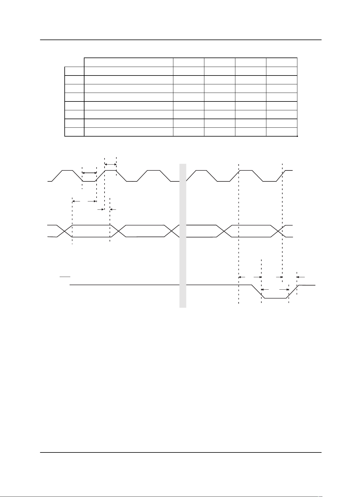
6.2 Serial Interface Timing
Parameter Min. Typ. Max. Units
t
PWH
Serial Clock “High” Pulse Width 250 ns
t
PWL
Serial Clock “Low” Pulse Width 250 ns
t
DS
Data Set-up Time 150 ns
t
DH
Data Hold Time 50 ns
t
LLO
Load/Latch Over Time 0 ns
t
LLD
Load/Latch Delay 200 ns
t
LLW
Load/Latch Pulse Width 150 ns
Serial Data Clock Frequency 2.0 MHz
Serial
Clock
Serial
Data
Load/Latch
t
t
t
t
t
PWL
PWH
DS
LLW
DH
D0
1ST
CLOCK
PULSE
14TH
CLOCK
PULSE
D13
D12
D1
t
LLD
t
LLO
Figure 4: Serial Timing Diagram
Page 11

Dual Digitally Controlled Amplifier 11 MX029
1998 MX-COM, INC. www.mxcom.com Tele: 800 638 5577 910 744 5050 Fax: 910 744 5054 Doc. # 20480096.008
4800 Bethania Station Road, Winston-Salem, NC 27105-1201 USA. All trademarks and service marks are held by their respective companies.
6.3 Packaging
PIN 1
A
B
ALTERNATIVE
PIN
LOCATION
MARKING
E
L
T
P
J
Y
C
H
0.303 (7.70)
PackageTolerances
TYP. MAX.MIN.
A
B
C
E
H
DIM.
J
P
Y
T
L
0.047 (1.20)----------
0.256 (6.50)
0° 8°
0.030 (0.75)
0.311 (7.90)
0.177 (4.50)
0.0256 (0.65)
0.020 (0.50)
0.248 (6.30)
0.006 (0.15)0.002 (0.05)
0.003 (0.08) 0.008 (0.20)
0.007 (0.17) 0.012 (0.30)
0.169 (4.30)
NOTE: All dimensions in inches (mm.)
Angles are in degrees
Figure 5: 24-pin TSSOP Mechanical Outline: Order as part no. MX029TN
PIN 1
A
B
ALTERNATIVE
PIN
LOCATION
MARKING
X
P
J
Y
C
K
H
E
L
T
W
Z
NOTE: All dimensions in inches (mm.)
Angles are in degrees
PackageTolerances
A
B
C
E
H
TYP.
MAX.MIN.
DIM.
J
P
X
W
T
Y
K
L
0.105 (2.67)0.093 (2.36)
0.419 (10.64)
45°
7°
0° 10°
0.050 (1.27)
0.041 (1.04)
0.413 (10.49)
0.299 (7.59)
0.050 (1.27)
0.016 (0.41)
0.390 (9.90)
0.020 (0.51)0.003 (0.08)
0.009 (0.23) 0.0125 (0.32)
0.013 (0.33) 0.020 (0.51)
0.395 (10.03)
0.286 (7.26)
Z
5°
5°
Figure 6: 16-pin SOIC Mechanical Outline: Order as part no. MX029DW
Page 12

Dual Digitally Controlled Amplifier 12 MX029
1998 MX-COM, INC. www.mxcom.com Tele: 800 638 5577 910 744 5050 Fax: 910 744 5054 Doc. # 20480096.008
4800 Bethania Station Road, Winston-Salem, NC 27105-1201 USA. All trademarks and service marks are held by their respective companies.
B
A
PIN 1
E1
T
E
K
H
F
J1
J
P
L
C
K1
PackageTolerances
NOTE: All dimensions in inches (mm.)
Angles are in degrees
TYP.
MAX.MIN.
A
B
C
E
E1
F
H
DIM.
J
J1
P
T
K1
K
L
0.230 (5.84)
0.291 (7.39)
0.415 (10.53)
0.200 (5.08)
0.767 (19.48)
0.165 (4.19)
0.100 (2.54)
0.115 (2.92)
0.370 (9.40)
0.300 (7.61) 0.317 (8.04)
0.70 (17.78)
0.018 (0.46)
0.053 (1.33)
0.075 (1.91)
0.080 (2.03)
0.080 (2.03)
0.753 (19.13)
0.285 (7.24)
0.0102 (0.259)
0.020 (0.51)
0.055 (1.39)
0.0098 (0.249)
Figure 7: 16-pin CDIP Mechanical Outline: Order as part no. MX029J
 Loading...