

Page 1
DATA BULLETIN
MX019
1998 MX-COM, INC. www.mxcom.com Tel: 800 638 5577 910 744 5050 Fax: 910 744 5054 Doc. # 20480077.006
4800 Bethania Station Road, Winston-Salem, NC 27105-1201 USA All trademarks and service marks are held by their respective companies
Quad Digital Control Amplifier
FEATURES APPLICATIONS
4 Digitally Controlled Amplifiers
15 Gain/Attenuation Steps
3 Amplifiers
± 3dB Range in 0.43dB Steps
1 'Volume' Amplifier
±14dB Range in 2dB Steps
8-Bit Serial Data Control
Output Mute Function
Gain Control Applications
Audio
Data
Telecommunications, Radio, & Industrial
Applications
2
3
3
3
4
4
SERIAL DATA
INPUT
LOAD/LATCH
LOAD/LATCH
CHIP ADDRESS
1
1
2
2
Ch1
Ch2
Ch4
Ch3
V
DD
V
BIAS
SERIAL CLOCK
INPUT
V
SS
8-BIT SERIAL DATA INPUT
CONTROLLED A UDIO OUTPUT LINES
VOLUME
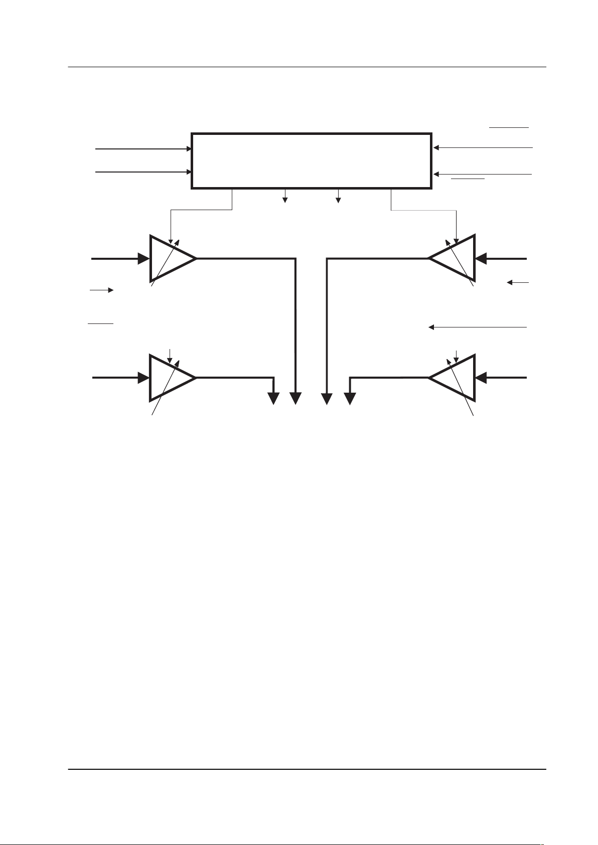
The MX019 Digitally Adjustable Amplifier Array replaces trimmer potentiometers and volume controls in
Cellular, LMR, Telephony and Communication applications where voice or data signals need adjustment.
The MX019 is a single-chip LSI consisting of four digitally controlled amplifier stages, each with 15 distinct
gain/attenuation steps. Control of each individual amplifier is by an 8-bit serial data stream. Three of the
amplifier stages offer a 3dB range in steps of 0.43dB, while the remaining amplifier offers a 14dB range in
steps of 2dB, and is suggested for volume control applications. Each amplifier includes a 16th 'Off' state
which, when applied, mutes the output audio from that channel. This array uses a Chip Select input to select
one of two MX019s in a system. The MX019 uses the host microprocessor to digitally control the set-up of all
audio levels during development, production/calibration, and operation. Such applications include:
1. Control, adjustment, and set-up of communications equipment by an Intelligent ATE without manual
intervention – eg. Deviation, Microphone and L/S Levels, RX Audio Level etc.
2. Automatic Dynamic Compensation of drift caused by variations in temperature, linearity, etc.
3. Fully automated servicing and re-alignment.
The MX019 is a low-power, single 5-volt CMOS device available in 24-pin TSSOP (MX019TN), 16-pin SOIC
(MX019DW), 16-pin CDIP (MX019J) and 16-pin PDIP (MX019P) package versions.
Page 2

Quad Digital Control Amplifier 2 MX019
1998 MX-COM, INC. www.mxcom.com Tel: 800 638 5577 910 744 5050 Fax: 910 744 5054 Doc. # 20480077.006
4800 Bethania Station Road, Winston-Salem, NC 27105-1201 USA All trademarks and service marks are held by their respective companies
CONTENTS
Section Page
1. Block Diagram 3
2. Signal List 4
3. External Components 5
4. General Description 5
4.1 Control Data and Timing 5
4.1.1 Data Loading 5
4.1.2 Timing 7
5. Application 8
6. Performance Specification 8
6.1 Electrical Performance 8
6.1.1 Absolute Maximum Ratings 8
6.1.2 Operating Limits 8
6.1.3 Operating Characteristics 9
6.2 Packaging 10
MX-COM, Inc. reserves the right to change specifications at any time and without notice.
Page 3
Quad Digital Control Amplifier 3 MX019
1998 MX-COM, INC. www.mxcom.com Tel: 800 638 5577 910 744 5050 Fax: 910 744 5054 Doc. # 20480077.006
4800 Bethania Station Road, Winston-Salem, NC 27105-1201 USA All trademarks and service marks are held by their respective companies
1. Block Diagram
2
3
3
3
4
4
SERIAL DATA
INPUT
LOAD/LATCH
LOAD/LATCH
CHIP ADDRESS
1
1
2
2
Ch1
Ch2
Ch4
Ch3
V
DD
V
BIAS
SERIAL CLOCK
INPUT
V
SS
8-BIT SERIAL DATA INPUT
CONTROLLED AUDIO OUTPUT LINES
VOLUME
Figure 1: Device Block Diagram
Page 4
Quad Digital Control Amplifier 4 MX019
1998 MX-COM, INC. www.mxcom.com Tel: 800 638 5577 910 744 5050 Fax: 910 744 5054 Doc. # 20480077.006
4800 Bethania Station Road, Winston-Salem, NC 27105-1201 USA All trademarks and service marks are held by their respective companies
2. Signal List
Pin No.
J/PDWTN
Name Description
1 1 Serial Clock This external clock pulse input is used to “clock in” the Control Data. See
Figure 3. This input has an internal 1M pullup resistor.
22
Load/
Latch
This input governs the loading and execution of the control data. During
serial data loading this input should be kept at a logical '0' to ensure that data
rippling past the latches has no effect. When all 8 bits have been loaded,
this input should be strobed '0 - 1 - 0' to latch the new data in. Data is
executed on the falling edge of the strobe. If the
Load
/Latch input is used
this pin should be left open circuit. This input has an internal 1M pullup
resistor.
34
LATCH/LOAD
This inverted Load/
Latch
input governs the loading and execution of control
data. During serial data loading this input should be kept at a logical '1' to
ensure that data rippling past the latches has no effect. When all 8 bits have
been loaded, this input should be strobed '1' - '0' - '1' to latch the new data in.
Data is executed on the rising edge of the strobe. If the Load/
Latch
input is
used this pin should be left open circuit. This input has an internal 1M
pulldown resistor.
4 5 Ch1 Input
Analog Inputs :
5 6 Ch2 Input These individual amplifier inputs are self-biasing; AC input analog signals
must be capacitively coupled to these pins, as shown in Figure 2.
6 7 Ch3 Input Note that amplifiers Ch1 to Ch4 are 'inverting amplifiers.'
7 8 Ch4 Input
812 V
SS
Negative supply rail (GND).
913 V
BIAS
The output of the on-chip bias circuitry, held at VDD/2. This pin should be
decoupled to V
SS
as shown in Figure 2.
10 14 Ch4 Output
Controlled Analog Outputs :
11 17 Ch3 Output These are individual "Gain Controlled" amplifier outputs. Ch1 to Ch3 range
from -3dB to +3dB in 0.43dB steps, Ch4 can be utilized as a volume control,
12 18 Ch2 Output ranging from -14dB to +14dB in 2.0dB steps. In the “OFF” mode there is no
13 19 Ch1 Output output from the selected amplifier.
14 20 Chip Address A logic input to select one of two MX019 ICs in a system (see Table 1). This
input has an internal 1M pulldown resistor.
15 23 Control Data
Input
Operation of the 4 amplifier channels (Ch1 – Ch4) is controlled by the 8 bits
of data entered serially at this pin. The data is entered (bit 7 to bit 0) on the
rising edge of the external Serial Clock. The data format is described in
Table 1, Table 2 and Figure 3. This input has an internal 1M pullup resistor.
16 24 V
DD
Positive supply rail. A single +5V power supply is required.
Page 5

Quad Digital Control Amplifier 5 MX019
1998 MX-COM, INC. www.mxcom.com Tel: 800 638 5577 910 744 5050 Fax: 910 744 5054 Doc. # 20480077.006
4800 Bethania Station Road, Winston-Salem, NC 27105-1201 USA All trademarks and service marks are held by their respective companies
3. External Components
V
DD
V
DD
C
6
C
1
C
2
C
3
C
4
C
5
V
SS
V
BIAS
1
2
3
4
5
6
7
8
16
15
14
13
12
11
10
9
SERIAL CLOCK INPUT
CONTROL DATA INPUT
CHIP ADDRESS
CHANNEL 1 OUTPUT
CHANNEL 2 OUTPUT
CHANNEL 3 OUTPUT
CHANNEL 4 OUTPUT
CHANNEL 1 INPUT
CHANNEL 2 INPUT
CHANNEL 3 INPUT
CHANNEL 4 INPUT
LOAD/LATCH
LOAD/LATCH
MX019J
C1 to C4 0.1µF ± 20%
C5 1.0µF ± 20%
C6 1.0µF ± 20%
Figure 2: Recommended External Components
Notes:
1. Channel Amplifiers 1 to 4 are inverting amplifiers.
2. Analog input capacitors C1 to C4 are only required for AC input signals, DC input signals do not
require these components.
4. General Description
4.1 Control Data and Timing
The gain of each amplifier block (Channel 1 to Channel 4) in the MX019 is set by a separate 8-bit data word
(bit 7 to bit 0). This 8-bit word, consisting of 4 Address bits (bit 7 to bit 4) and 4 Gain Control bits (bit 3 to bit
0), is loaded to the Control Data Input in serial format using the external data clock.
4.1.1 Data Loading
The 8-bit data word is loaded bit 7 first and bit 0 last.
Bit 7 must be a logic “1” to address the chip.
If bit 7 in the word is a logic “0” that 8-bit word will not be executed. The Chip Address input permits the use of
two devices in a system by indicating to the chip what its address is, a “1” or a “0.” Bit 6 in the address section
of the control word is then used to select which device is being controlled. Figure 3 shows the timing
information required to load and operate this device.
Data is loaded to the MX019 on the rising edge of the Serial Clock. Loaded data is executed on the falling
(rising) edge of the Load/
Latch (Load
/Latch) pulse.
Table 1 shows the format of each 4-bit Address word, Table 2 shows the format of each Gain Control word
with Figure 3 describing the data loading operation and timing.
Page 6

Quad Digital Control Amplifier 6 MX019
1998 MX-COM, INC. www.mxcom.com Tel: 800 638 5577 910 744 5050 Fax: 910 744 5054 Doc. # 20480077.006
4800 Bethania Station Road, Winston-Salem, NC 27105-1201 USA All trademarks and service marks are held by their respective companies
Bit 7
MSB
Bit 6 Bit 5 Bit 4
LSB
Channel
Address
Chip
Address
Chip
Number
1
1
1
1
0
0
0
0
0
0
1
1
0
1
0
1
1
2
3
4
0
0
0
0
Chip 1
1
1
1
1
1
1
1
1
0
0
1
1
0
1
0
1
1
2
3
4
1
1
1
1
Chip 2
Table 1: Address Bits Format
Bit 3
MSB
Bit2 Bit 1 Bit 0
LSB
Stage 1, 2, 3
(0.43dB)
Stage 4
(2.0dB)
0000 OFF OFF
0001 -3.0 -14.0dB
0010 -2.571 -12.0
0011 -2.143 -10.0
0100 -1.714 -8.0
0101 -1.286 -6.0
0110 -0.857 -4.0
0111 -0.428 -2.0
1000 0 0
1001 0.428 2.0
1010 0.857 4.0
1011 1.286 6.0
1100 1.714 8.0
1101 2.143 10.0
1110 2.571 12.0
1111 3.0 14.0
Table 2: Gain Control Bits Format
Page 7

Quad Digital Control Amplifier 7 MX019
1998 MX-COM, INC. www.mxcom.com Tel: 800 638 5577 910 744 5050 Fax: 910 744 5054 Doc. # 20480077.006
4800 Bethania Station Road, Winston-Salem, NC 27105-1201 USA All trademarks and service marks are held by their respective companies
4.1.2 Timing
Timing (Figure 3) Min. Typ. Max. Units
Serial Clock "High" Pulse Width (t
PWH
) 250 ns
Serial Clock "Low" Pulse Width (t
PWL
) 250 ns
Data Set-up Time (tDS) 150 ns
Data Hold Time (tDH) 50.0 ns
Load/Latch Pulse Width (t
LLW
) 150 ns
Load/Latch Delay (t
LLD
) 200 ns
Load/Latch Over (t
LLO
)0.0ns
Serial Data Clock Frequency 2.0 MHz
SERIAL DATA CLOCK
t
PWL
t
PWH
t
DS
Loaded Last
Logic '1'
Loaded
First
BIT 7
BIT 6
BIT 1
BIT 0
t
DH
SERIAL DATA IN
(ONE 8-BIT WORD)
t
LLO
8th
Clock
Pulse
Next
Clock
Pulse
t
LLD
t
LLW
LOAD/LATCH
LOAD/LATCH
Figure 3: Serial Control Data Loading Diagram
Page 8

Quad Digital Control Amplifier 8 MX019
1998 MX-COM, INC. www.mxcom.com Tel: 800 638 5577 910 744 5050 Fax: 910 744 5054 Doc. # 20480077.006
4800 Bethania Station Road, Winston-Salem, NC 27105-1201 USA All trademarks and service marks are held by their respective companies
5. Application
To avoid excess noise and instability you should take note of the following:
1. A noisy or badly regulated power supply can cause instability and/or variance of selected gains.
2. Care should be taken on the design and layout of the printed circuit board.
3. All external components (Figure 2) should be kept close to the MX019 package.
4. Inputs and outputs should be shielded wherever possible.
5. Tracks should be kept short.
6. Analog tracks should not run parallel to digital tracks.
7. A "Ground Plane" connected to V
SS
will assist in eliminating external pick-up on the channel input and
output pins.
8. Do not run high-level output tracks close to low-level input tracks.
6. Performance Specification
6.1 Electrical Performance
6.1.1 Absolute Maximum Ratings
Exceeding these maximum ratings can result in damage to the device.
General Min. Max. Units
Supply Voltage -0.3 7.0 V
Input Voltage at any pin (ref VSS = 0V) -0.3 (VDD + 0.3) V
Current
V
DD
±30 mA
V
SS
±30 mA
Any other pins ±20 mA
J/P/DW Packages
Total Device Dissipation @ T
AMB
25°C 800 mW
Derating above 25°C 10 mW/°C above 25°C
TN Packages
Total Device Dissipation @ T
AMB
25°C 500 mW
Derating above 25°C 9 mW/°C above 25°C
Operating Temperature -40 85 °C
Storage Temperature -55 125 °C
6.1.2 Operating Limits
Correct operation of the device outside these limits is not implied.
Min. Typ. Max. Units
V
DD
4.5 5.0 5.5 V
Operating Temperature -40 85 °C
Page 9

Quad Digital Control Amplifier 9 MX019
1998 MX-COM, INC. www.mxcom.com Tel: 800 638 5577 910 744 5050 Fax: 910 744 5054 Doc. # 20480077.006
4800 Bethania Station Road, Winston-Salem, NC 27105-1201 USA All trademarks and service marks are held by their respective companies
6.1.3 Operating Characteristics
For the following conditions unless otherwise specified:
V
DD
= 5.0V, T
AMB
= 25°C
Audio Level 0dB ref. = 775mV
RMS
, Amplifier Gain Set = 0dB
Notes Min. Typ. Max Units
Static Values
Supply Current 1.5 mA
Dynamic Values
Control Functions
Input Logic '1' 3.5 V
Input Logic '0' 1.5 V
Digital Input Impedances 0.5 1.0
M
Amplifier Stages (General)
Bandwidth (-3dB) 20.0 kHz
Output Impedance 1.0
k
Total Harmonic Distortion 1 0.35 0.5 %
Output Noise Level (per stage) 2 180.0 400.0 µV
RMS
Onset of Clipping 3 1.73 V
RMS
Gain Variation 4 0.1 dB
Interstage Isolation 60.0 dB
“Trimmer” Stages (Ch1 – Ch3)
Gain -3.0 +3.0 dB
Gain per Step (15 in No.) 0.43 dB
Step Error 0.2 dB
Input Impedance 100.0
k
“Volume” Stage (Ch4)
Gain -14.0 +14.0 dB
Gain per Step (15 in No.) 2.0 dB
Step Error 0.4 dB
Input Impedance 50.0
k
Operating Characteristics Notes:
1. Gain Set 0dB, Input Level 1kHz -3.0dB (549mVrms).
2. With an a.c short-circuit input, measured in a 30kHz bandwidth.
3. See Figure 4.
4. Over the temperature and supply voltage range.
Page 10

Quad Digital Control Amplifier 10 MX019
1998 MX-COM, INC. www.mxcom.com Tel: 800 638 5577 910 744 5050 Fax: 910 744 5054 Doc. # 20480077.006
4800 Bethania Station Road, Winston-Salem, NC 27105-1201 USA All trademarks and service marks are held by their respective companies
INPUT LEVEL dB
SINAD (dB)
30
40
50
60
-40
-30 -20 -10
0
10.0 25.0 75.0 250.0 775.0
1000.0
1730.0
-17
110.0
mVrms
7.0
Input Frequency = 1.0kHz
Figure 4: SINAD vs Input Level – Typical Values
6.2 Packaging
PIN 1
A
B
ALTERNATIVE
PIN
LOCATION
MARKING
E
L
T
P
J
Y
C
H
0.303 (7.70)
PackageTolerances
TYP. MAX.MIN.
A
B
C
E
H
DIM.
J
P
Y
T
L
0.047 (1.20)----------
0.256 (6.50)
0° 8°
0.030 (0.75)
0.311 (7.90)
0.177 (4.50)
0.0256 (0.65)
0.020 (0.50)
0.248 (6.30)
0.006 (0.15)0.002 (0.05)
0.003 (0.08) 0.008 (0.20)
0.007 (0.17) 0.012 (0.30)
0.169 (4.30)
NOTE: All dimensions in inches(mm.)
Angles are in degrees
Figure 5: 24-pin TSSOP Mechanical Outline: Order as part no. MX019TN
Page 11

Quad Digital Control Amplifier 11 MX019
1998 MX-COM, INC. www.mxcom.com Tel: 800 638 5577 910 744 5050 Fax: 910 744 5054 Doc. # 20480077.006
4800 Bethania Station Road, Winston-Salem, NC 27105-1201 USA All trademarks and service marks are held by their respective companies
PIN 1
A
B
ALTERNATIVE
PIN
LOCATION
MARKING
X
P
J
Y
C
K
H
E
L
T
W
Z
NOTE: All dimensions in inches(mm.)
Angles are in degrees
PackageTolerances
A
B
C
E
H
TYP.
MAX.MIN.
DIM.
J
P
X
W
T
Y
K
L
0.105 (2.67)0.093 (2.36)
0.419 (10.64)
45°
7°
0° 10°
0.050 (1.27)
0.041 (1.04)
0.413 (10.49)
0.299 (7.59)
0.050 (1.27)
0.016 (0.41)
0.390 (9.90)
0.020 (0.51)0.003 (0.08)
0.009 (0.23) 0.0125 (0.32)
0.013 (0.33) 0.020 (0.51)
0.395 (10.03)
0.286 (7.26)
Z
5°
5°
Figure 6: 16-pin SOIC Mechanical Outline: Order as part no. MX019DW
PackageTolerances
NOTE: All dimensions in inches(mm.)
Angles are in degrees
TYP. MAX.MIN.
A
B
C
E
E1
H
DIM.
J
J1
P
Y
T
K
L
0.200 (5.06)
0.262 (6.63)
0.390 (9.91).
7°
0.150 (3.81)
0.810 (20.57)
0.135 (3.43)
0.100 (2.54)
0.121 (3.07)
0.300 (7.62)
0.290 (7.37) 0.325 (8.26)
0.015 (0.38) 0.070 (1.77)
0.008 (0.20) 0.015 (0.38)
0.014 (0.35) 0.023 (0.58)
0.040 (1.02) 0.065 (1.65)
0.056 (1.42) 0.064 (1.63)
0.740 (18.80)
0.240 (6.10)
B
A
PIN 1
E
Y
E1
T
K
H
J1
J
C
P
L
Figure 7: 16-pin PDIP Mechanical Outline: Order as part no. MX019P
Page 12

Quad Digital Control Amplifier 12 MX019
1998 MX-COM, INC. www.mxcom.com Tel: 800 638 5577 910 744 5050 Fax: 910 744 5054 Doc. # 20480077.006
4800 Bethania Station Road, Winston-Salem, NC 27105-1201 USA All trademarks and service marks are held by their respective companies
B
A
PIN 1
E1
T
E
K
H
F
J1
J
P
L
C
K1
PackageTolerances
NOTE: All dimensions in inches(mm.)
Angles are in degrees
TYP.
MAX.MIN.
A
B
C
E
E1
F
H
DIM.
J
J1
P
T
K1
K
L
0.230 (5.84)
0.291 (7.39)
0.415 (10.53)
0.200 (5.08)
0.767 (19.48)
0.165 (4.19)
0.100 (2.54)
0.115 (2.92)
0.370 (9.40)
0.300 (7.61) 0.317 (8.04)
0.70 (17.78)
0.018 (0.46)
0.053 (1.33)
0.075 (1.91)
0.080 (2.03)
0.080 (2.03)
0.753 (19.13)
0.285 (7.24)
0.0102 (0.259)
0.020 (0.51)
0.055 (1.39)
0.0098 (0.249)
Figure 8: 16-pin CDIP Mechanical Outline: Order as part no. MX019J
 Loading...