

Page 1
DATA BULLETIN
MX014
Voice Band inverter
Features Applications
•
CTCSS Compatible
•
Fixed Frequency Inversion
•
Low Power CMOS
TX Audio Feedback
TX Audio In
BIAS
RX Audio In
RX Audio Feedback
Rx Path
RX Path
6dB/Octave
Pre-emphasis
10dB Gain
Bandpass
Filter
300-3033 Hz
Filsav1
Filter
BALMOD
Carrier
•
Land Mobile Radio Systems
•
Community Repeaters
PathInv ert
Bandpass
Filter
300-3033 Hz
BPF Out
6dB/Octave
De-emphasis
Filsav1
Filsav2
DEEMP Out
TX
TX BufferIn
RX BufferIn
BIAS
RX Path
TX Audio Out
TX
RX Audio Out
Clock
Clock
PTT
PTT
RX Audio Enable
RX Audio Enable
PTL
PTL
Privacy Enable
3333 Hz
LOGIC
Carrier
Filsav1
Filsav2
RX Path
EMPSAV
TX
PathInv ert
CLK
3333 Hz
CLK Generator
V
DD
V
SS
BIAS
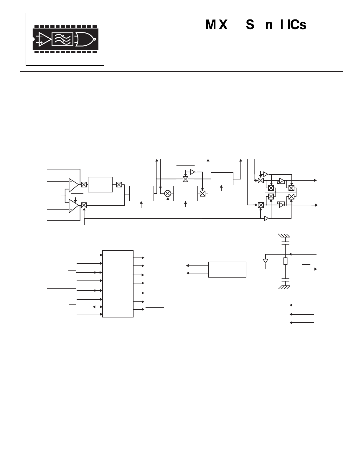
The MX014 Voice Band Inverter gives the security of private voice communications to land mobile radio users, as well as
to the users of other shared radio channel systems. Designed for use in half-duplex systems, the MX014 exchanges high
and low frequencies in the voiceband and renders transmitted messages unintelligible. This privacy function is achieved
by a single frequency inversion. When used with CTCSS,
SQUELCH
Pvt
TM
privacy adapter operation is achieved.
Sharp cut-off in the internal voiceband filters permits operation with CTCSS and similar sub-audio signaling schemes. This
results in high quality recovered audio.
The core of the MX014 consists of two audio band pass filters and a balanced modulator. The device uses a
programmable clock divider which controls the carrier and filter cut-off frequencies. Control of the RX/TX, PTL and
privacy function is by pin selection.
The MX014 operates from a single 5V supply and uses a 4 MHz crystal oscillator to ensure the correct pitch in recovered
speech. Signal coupling and decoupling are the only external components needed. The device is available in 24-pin
PLCC (MX014LH), 24-pin PDIP (MX014P) and 24-pin CDIP (MX014J) packages.
1997 MX•COM, INC. www.mxcom.com Tele: 800 638 5577 910 744 5050 Fax: 910 744 5054 Doc. # 20480013.006
4800 Bethania Station Road, Winston-Salem, NC 27105-1201 USA All trademarks and service marks are held by there respective companies.
Page 2

Voice Band Inverter 2 MX014
CONTENTS
Section Page
1. Block Diagram.................................................................................................................................. 3
2. Signal List......................................................................................................................................... 4
3. External Components...................................................................................................................... 5
4. Application ....................................................................................................................................... 6
5. Performance Specification.............................................................................................................. 8
5.1 Electrical Performance.............................................................................................................................. 8
5.1.1 Absolute Maximum Ratings...............................................................................................................................8
5.1.2 Operating Limits.................................................................................................................................................8
5.1.3 Operating Characteristics ..................................................................................................................................8
5.2 Packaging ................................................................................................................................................ 10
MX•COM, Inc. reserves the right to change specifications at any time and without notice.
1997 MX•COM, INC. www.mxcom.com Tele: 800 638 5577 910 744 5050 Fax: 910 744 5054 Doc. # 20480013.006
4800 Bethania Station Road, Winston-Salem, NC 27105-1201 USA All trademarks and service marks are held by there respective companies.
Page 3
Voice Band Inverter 3 MX014
1. Block Diagram
TX Audio Feedback
TX Audio In
BIAS
RX Audio In
RX Audio Feedback
RX Audio Enable
RX Audio Enable
Privacy Enable
Rx Path
PTT
PTT
PTL
PTL
RX Path
3333 Hz
6dB/Octave
Pre-emphasis
10dB Gain
LOGIC
Bandpass
Filter
300-3033 Hz
Filsav 1
Carrier
Filsav 1
Filsav 2
RX Path
EMPSAV
TX
Path Invert
Filter
BALMOD
Carrier
Path Invert
Bandpass
Filter
300-3033 Hz
Filsav 2
CLK
3333 Hz
BPF Out
6dB/Octave
De-emphasis
Filsav 1
CLK Generator
TX
DEEMP Out
TX Buffer In
RX Buffer In
BIAS
RX Path
TX
V
DD
V
SS
BIAS
TX Audio Out
RX Audio Out
Clock
Clock
Figure 1: Device Block Diagram
1997 MX•COM, INC. www.mxcom.com Tele: 800 638 5577 910 744 5050 Fax: 910 744 5054 Doc. # 20480013.006
4800 Bethania Station Road, Winston-Salem, NC 27105-1201 USA All trademarks and service marks are held by there respective companies.
Page 4
Voice Band Inverter 4 MX014
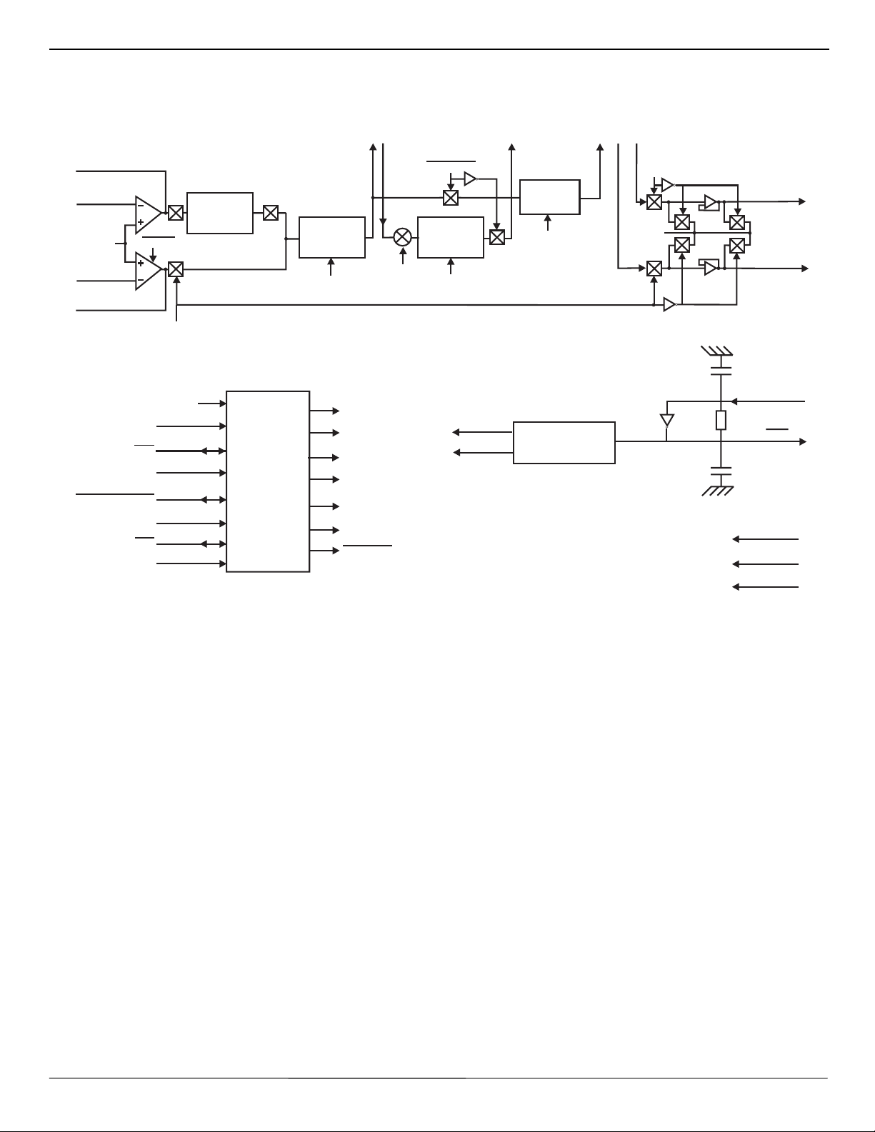
2. Signal List
Pin No. Name Description
1 XTAL An external 4MHz clock can be applied to this input. The clock circuit on chip has a resistor
and capacitors so that only one external crystal is required.
2
XTAL
3PTT
4
PTT
5PTL
6
PTL
7 RXAUDEN
8
RXAUDEN
9 PRIVEN Privacy Enable controls the input action of the balanced modulator by switching the carrier
10 RXOUT This is the receive audio output pin. It is biased at VDD/2 when in the TX mode.
11 TXOUT This is the “send” voice output pin. It is biased at VDD/2 when in RX mode.
12 V
SS
13 BPFOUT For a gain of one in the RX Output stage, these two pins are wire linked together. However,
14 RXBIN
15 DEMPOUT The pre-emphasis circuit has a 10dB gain at 1 kHz. Additional gain, or attenuation can
16 TXBIN
17 BIAS This is the internally generated VDD/2 decoupling pin.
18 FILTR This filter is the output of the Input Audio BPF and must be a.c. coupled into the Balanced
19 BALMOD This is the input to the balanced modulator. It must be a.c. coupled to the Filter Output.
20 RXIN This is a negative input of an op-amp at the input of the RX path. It can be used, along with
21 RXFB RX Audio Feedback is the output of an op-amp at the input of the RX path. See RXIN.
22 TXIN The negative input of an op-amp at the input of the TX path. It can be used, along with TX
23 TXFB TX Audio Feedback is the output of an op-amp at the input of the TX path. See TXIN.
24 V
DD
This is the inverted 4MHz clock output for use when a crystal oscillator is used, or as a buffer
for driving other clocked devices.
Push To Talk is an input with a 3MΩ pull-down resistor.
This is the inverted PTT output. It has a 100kΩ output impedance.
Push To Listen is an input with a 3MΩ pull-down resistor.
Push To Listen
is the inverted output of PTL; it has a 100kΩ output impedance.
RX Audio Enable is an input with a 3MΩ pull-down resistor.
RX Audio Enable
is the inverted output of RX Audio Enable; it has a 100kΩ output impedance.
clock. When audio signals are inverted, the signal path gain is adjusted automatically to
compensate for the upper sideband loss. It contains a 3MΩ pull-down resistor.
The negative supply pin (ground).
if gain is introduced at the RX input, attenuation may be introduced at the RX Output using
these pins and two resistors.
be introduced as in the RX path.
Modulator Input through a 0.1µF capacitor.
RX Audio Feedback and two external resistors, to increase the signal to its optimum level prior
to frequency inversion/filtering. This may improve the S/N.
Audio Feedback and two external resistors, to increase the signal to its optimum level prior to
frequency inversion/filtering. This may improve S/N.
The positive supply pin.
Table 1: Signal List
1997 MX•COM, INC. www.mxcom.com Tele: 800 638 5577 910 744 5050 Fax: 910 744 5054 Doc. # 20480013.006
4800 Bethania Station Road, Winston-Salem, NC 27105-1201 USA All trademarks and service marks are held by there respective companies.
Page 5

Voice Band Inverter 5 MX014
g
g
g
g
3. External Components
Configuration for Radios with
Existing Pre- and De-emphasis.
X1
1
MX014
XTAL
2
XTAL
3
PTT
4
PTT
5
PTL
6
7
8
9
10
11
12
PTL
RXAUDEN
RXAUDEN
PRIVEN
RXOUT
TXOUT
V
BALMOD
DEMPOUT
SS
TX Attenuation
For a
ain of 1, R8 , R7 0
BPFOUT
24
V
DD
23
TXFB
22
TXIN
21
RXFB
20
RXIN
19
18
FILTR
17
BIAS
TXBIN
16
15
14
RXBIN
13
Figure 2: External Components Connections
R8
=
+
R7 R8
=∞ =
R1
R3
R7
R5
C4
V
DD
R2
R4
C3
R8
R6
C1
C2
Bias
Bias
TX Channel
RX Channel
For Use in Radios without
Pre- and De-emphasis.
1
MX014
X1
TX Attenuation
For a
XTAL
2
XTAL
3
PTT
4
PTT
5
PTL
6
PTL
7
RXAUDEN
8
RXAUDEN
9
PRIVEN
10
11
12
RXOUT
TXOUT
V
SS
DEMPOUT
ain of 1, R9 0, R10
24
V
DD
23
TXFB
TXIN
RXFB
RXIN
BALMOD
FILTR
BIAS
TXBIN
RXBIN
BPFOUT
=
R9 R10
R10
R1
22
21
R3
20
19
18
17
C4
16
15
R11
14
13
+
==∞
R9
V
DD
R2
R4
C3
R10
R12
C1
C2
TX Channel
RX Channel
Bias
Bias
RX Attenuation
For a
ain of 1, R6 , R5 0
R6
=
R5 R6
=∞ =
+
RX Attenuation
For a
ain of 1, R11 0, R12
R12
=
+
R11 R12
==∞
Table 2: Gain and Attentuation Calculations
Recommended External Component Notes:
1. Component Values: C1- C3 = 0.1 µF, C4 = 1.0 µF, X1 = 4 MHz crystal
2. R1 to R12 values will depend on the configuration and the gain or attenuation required. However R1, R3, R5, R7,
and R11 should be 100 kΩ or greater. To add gain or attenuate, use R5-R12 as shown. See pin descriptions for
more information.
3. For best results, a crystal oscillator design should drive the clock inverter input with signal levels of at least 40% of
VDD, peak to peak. Tuning fork crystals generally cannot meet this requirement. To obtain crystal oscillator
design assistance, consult your crystal manufacturer.
1997 MX•COM, INC. www.mxcom.com Tele: 800 638 5577 910 744 5050 Fax: 910 744 5054 Doc. # 20480013.006
4800 Bethania Station Road, Winston-Salem, NC 27105-1201 USA All trademarks and service marks are held by there respective companies.
Page 6

Voice Band Inverter 6 MX014
4. Application
BIAS
R8
C1
R7
TX Channel
TX Audio Feedback
C1
RX Channel
R2
C2
R1
TX Audio In
R4
BIAS
R3
+
BIAS
RX Audio In
RX Audio Feedback
6dB/Octave
Pre-emphasis
+
-
10dB Gain
Note: Dotted Lines contain on-chip functions
Bandpass
Filter
300-3033 Hz
Bandpass
Filter
300-3033 Hz
Filter
C3
Filter
BALMOD
Carrier
BALMOD
Carrier
Bandpass
300-3033 Hz
Path Invert
Bandpass
Filter
300-3033 Hz
Path Invert
Filter
BPF Out
-6dB/Octave
De-emphasis
R5
DEEMP Out
BIAS
TX Audio Out
TX Buffer In
R6
RX Buffer In
RX Audio Out
TX
RX
Figure 3: Voice Privacy Application (Add-on)
1997 MX•COM, INC. www.mxcom.com Tele: 800 638 5577 910 744 5050 Fax: 910 744 5054 Doc. # 20480013.006
4800 Bethania Station Road, Winston-Salem, NC 27105-1201 USA All trademarks and service marks are held by there respective companies.
Page 7

Voice Band Inverter 7 MX014
BIAS
R10
C1
R9
TX Channel
TX Audio Feedback
C1
RX Channel
R2
R1
TX Audio In
C2
R4
BIAS
+
RX Audio In
R3
RX Audio Feedback
Pre-emphasis
BIAS
6dB/Octave
10dB Gain
+
-
Note: Dotted Lines contain on-chip functions
Bandpass
Filter
300-3033 Hz
Bandpass
Filter
300-3033 Hz
Filter
C3
Filter
BALMOD
Carrier
BALMOD
Carrier
PathInvert
Bandpass
Filter
300-3033 Hz
PathInvert
Bandpass
Filter
300-3033 Hz
BPF Out
-6dB/Octave
De-emphasis
R11
DEEMP Out
TX Audio Out
TX BufferIn
BIAS
R12
RX BufferIn
RX Audio Out
TX
RX
Figure 4: Voice Processing Application (OEM)
1997 MX•COM, INC. www.mxcom.com Tele: 800 638 5577 910 744 5050 Fax: 910 744 5054 Doc. # 20480013.006
4800 Bethania Station Road, Winston-Salem, NC 27105-1201 USA All trademarks and service marks are held by there respective companies.
Page 8

Voice Band Inverter 8 MX014
5. Performance Specification
5.1 Electrical Performance
5.1.1 Absolute Maximum Ratings
Exceeding these maximum ratings can result in damage to the device.
General Min. Max. Units
Supply Voltage -0.3 7.0 V
Input Voltage at any pin
(ref. VSS + 0 V) -0.3 (VDD + 0.3 ) V
Current:
V
DD
V
SS
Any other pin 20 mA
J / P / LH Packages
Maximum Device Dissipation at T
= 25°C 800 mW
AMB
Derating above 25°C 10 mW/°C above 25°C
Operating Temperature Range: -40 85 °C
Storage Temperature Range: -55 125 °C
30 mA
30 mA
5.1.2 Operating Limits
Correct operation of the device outside these limits is not implied.
Min. Typ. Max. Units
V
DD
4.5 5.0 5.5 V
Clock Frequency 4.0 MHz
Operating Temperature -40 85 °C
5.1.3 Operating Characteristics
For the following conditions unless otherwise specified:
V
= 5.0V at T
DD
Clock Frequency = 4.0MHz, 0dB reference = 300mV
exceed 300mV
= 25°C
AMB
at 1kHz in Tx and 500mV
RMS
(Note: Measured at pin 18, the FILTR output. This pin must not
RMS
at any frequency in Rx, or clipping may occur. The difference in levels is
RMS
due to the pre-emphasis filter in the Tx path.
Notes Min. Typ. Max Units
Static Values
Supply Current:
RX/TX Operating (Private) 11.0 mA
RX/TX Operating (Clear) 8.0 mA
Standby 4 1.8 mA
Audio Input Impedance 10
Audio Output Impedance 5 0.5
Digital Output Impedance(Pulldown) 1
Digital I/O Impedance 100
Input Logic “1” 70% V
Input Logic “0” 30% V
M
M
Ω
Ω
k
Ω
Ω
k
DD
DD
1997 MX•COM, INC. www.mxcom.com Tele: 800 638 5577 910 744 5050 Fax: 910 744 5054 Doc. # 20480013.006
4800 Bethania Station Road, Winston-Salem, NC 27105-1201 USA All trademarks and service marks are held by there respective companies.
Page 9

Voice Band Inverter 9 MX014
Notes Min. Typ. Max Units
RX Clear Performance
Total Harmonic Distortion 1 2 5 %
Output Noise Level 2 2 mV
RMS
Passband Gain 0 dB
Passband Ripple (300-3033 Hz) 1 -3 +2 dB
Stopband Attenuation
(fin > 3333 Hz) 20 dB
(fin > 3633 Hz) 45 dB
(fin < 250 Hz) 42 dB
RX Inverted
Total Harmonic Distortion 1,3 4 %
Output Noise Level 2,3 4 mV
RMS
Passband Ripple (300 - 3033 Hz) 3 4 dB
Stopband Attenuation
(fin > 3333 Hz) 50 dB
(fin > 3633 Hz) 60 dB
Highpass Attenuation
(fin < 250 Hz) 60 dB
TX Clear
Total Harmonic Distortion 1 2 5 %
Output Noise Level 2 2 mV
rms
Passband Gain
(fin = 300 - 3033 Hz) 1 0 dB
Passband ripple
(fin = 300 - 3033 Hz) 1 4 dB
Stopband Attenuation
(fin > 3333 Hz) 2 20 dB
(fin > 3633 Hz) 45 dB
(fin < 250 Hz) 42 dB
TX Inverted
Total Harmonic Distortion 1,3 4 %
Output Noise Level 2 4 mV
rms
Passband Ripple
(fin = 300 - 3333 Hz) 1,3 4 dB
Stopband Attenuation
(fin > 3333 Hz) 3 50 dB
(fin > 3633 Hz) 3 60 dB
(fin < 250 Hz) 3 60 dB
Pre-Emphasis
Frequency Response 6 dB/Octave
Gain at 1 kHz 10 dB
De-emphasis
Frequency response -6 dB/Octave
Gain at 1 kHz 0 dB
1997 MX•COM, INC. www.mxcom.com Tele: 800 638 5577 910 744 5050 Fax: 910 744 5054 Doc. # 20480013.006
4800 Bethania Station Road, Winston-Salem, NC 27105-1201 USA All trademarks and service marks are held by there respective companies.
Page 10

Voice Band Inverter 10 MX014
Operating Characteristics Notes:
1. Input signal = 1kHz tone 0dB (300 mV
RMS
)
2. Input AC short circuit, audio path enabled. Measured in 30 kHz band
3. Due to frequency inversion (and pre- and de-emphasis), this refers to deviation from expected ideal response
4. Standby occurs in RX with RX Audio Enable = 0, RX Audio Enable = 1, and PTL = 1
5. TX Audio Out and RX Audio Out only
5.2 Packaging
D
E
B
Y
A
W
W
PIN 1
P
G
C
K
J
T
H
PackageTolerances
TYP. MAX.MIN.DIM.
0.380 (9.61)
A
0.380 (9.61)
B
0.128 (3.25)
C
0.417 (10.60)
D
0.417 (10.60)
E
F
G
H
J
0.047 (1.19)
K
0.049 (1.24)
P
0.006 (0.152)
T
30°
W
Y
NOTE: All dimensions in inches (mm.)
0.250 (6.35)
0.250 (6.35)
0.023 (0.58)
Angles are in degrees
0.409 (10.40)
0.409 (10.40)
0.146 (3.70)
0.435 (11.05)
0.435 (11.05)
0.022 (0.55)0.018 (0.45)
0.048 (1.22)
0.051 (1.30)
0.009 (0.22)
45°
6°
F
Figure 5: 24-pin PLCC Mechanical Outline: Order as part no. MX014LH
1997 MX•COM, INC. www.mxcom.com Tele: 800 638 5577 910 744 5050 Fax: 910 744 5054 Doc. # 20480013.006
4800 Bethania Station Road, Winston-Salem, NC 27105-1201 USA All trademarks and service marks are held by there respective companies.
Page 11

Voice Band Inverter 11 MX014
A
PIN1
PIN1
K
H
L
A
E
B
B
PP
JJ
J1J1
C
C
E1
E1
Y
E
T
T
PackageTolerances
TYP. MAX.MIN.DIM.
1.200 (30.48)
A
0.500 (12.70)
B
0.151 (3.84)
C
0.600 (15.24)
E
0.590 (14.99) 0.625 (15.88)
E1
0.015 (0.38) 0.045 (1.14)
H
0.015 (0.38) 0.023 (0.58)
J
0.040 (1.02) 0.065 (1.65)
J1
0.066 (1.67) 0.074 (1.88)
K
0.121 (3.07)
L
P
0.008 (0.20) 0.015 (0.38)
T
Y
NOTE: All dimensions in inches (mm.)
0.100 (2.54)
Angles are in degrees
1.270 (32.26)
0.555 (14.04)
0.220 (5.59)
0.670 (17.02)
0.160 (4.05)
7°
PIN1
K
H
L
Figure 6: 24-pin PDIP Mechanical Outline: Order as part no. MX014P
A
B
E1
E
T
C
K1
P
J
J1
F
Pac kageTolerances
DIM.
1.240 (31.50)
A
0.514 (13.06)
B
0.165 (4.19)
C
0.600 (15.23)
E
0.594 (15.09) 0.615 (15.61)
E1
F
H
J
J1
0.050 (1.27)
K
0.074 (1.88)
K1
0.115 (2.92)
L
P
0.0094 (0.239)
T
NOTE: All dimensions in inches (mm.)
Angles are in degrees
TYP. MAX.MIN.
1.260 (32.00)
0.583 (14.79)
0.230 (5.84)
0.670 (17.00)
1.100 (27.94)
0.02 (0.51)
0.018 (0.46)
0.055 (1.39)
0.080 (2.03)
0.080 (2.03)
0.200 (5.08)
0.10 (2.54)
0.0106 (0.269)
Figure 7: 24-pin CDIP Mechanical Outline: Order as part no. MX014J
1997 MX•COM, INC. www.mxcom.com Tele: 800 638 5577 910 744 5050 Fax: 910 744 5054 Doc. # 20480013.006
4800 Bethania Station Road, Winston-Salem, NC 27105-1201 USA All trademarks and service marks are held by there respective companies.
 Loading...